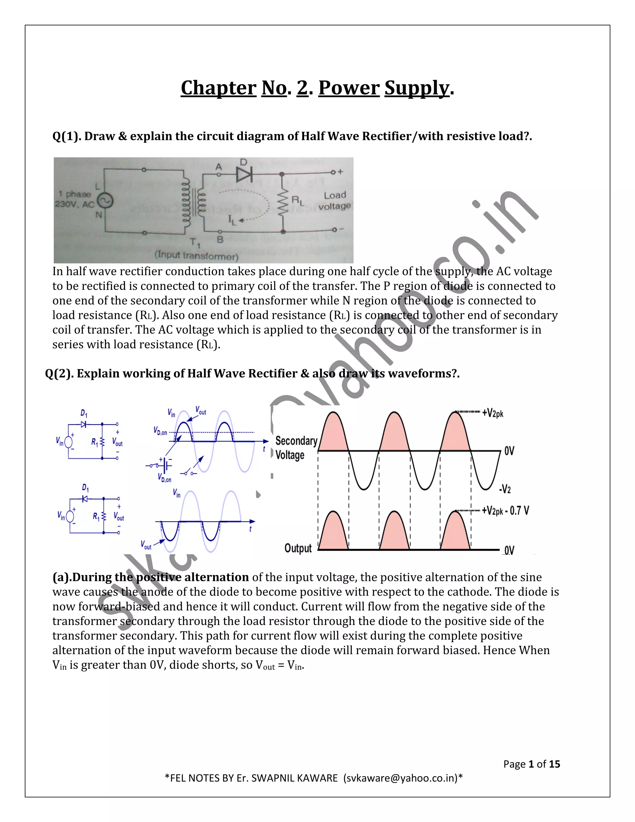
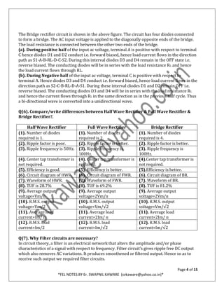
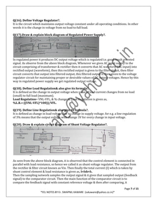
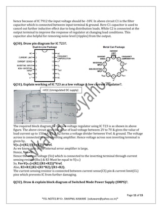
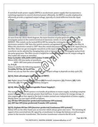
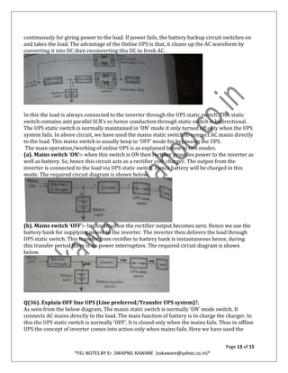
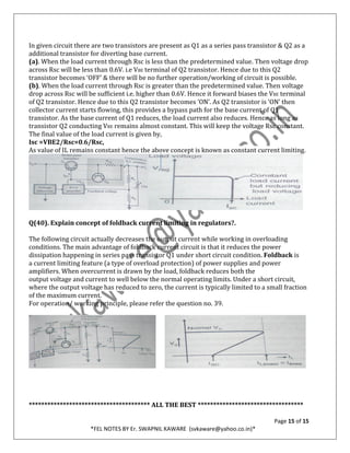
SlideShare a Scribd company logo
Page 1 of 15
*FEL NOTES BY Er. SWAPNIL KAWARE (svkaware@yahoo.co.in)*
Chapter No. 2. Power Supply.
Q(1). Draw & explain the circuit diagram of Half Wave Rectifier/with resistive load?.
In half wave rectifier conduction takes place during one half cycle of the supply, the AC voltage
to be rectified is connected to primary coil of the transfer. The P region of diode is connected to
one end of the secondary coil of the transformer while N region of the diode is connected to
load resistance (RL). Also one end of load resistance (RL) is connected to other end of secondary
coil of transfer. The AC voltage which is applied to the secondary coil of the transformer is in
series with load resistance (RL).
Q(2). Explain working of Half Wave Rectifier & also draw its waveforms?.
(a).During the positive alternation of the input voltage, the positive alternation of the sine
wave causes the anode of the diode to become positive with respect to the cathode. The diode is
now forward-biased and hence it will conduct. Current will flow from the negative side of the
transformer secondary through the load resistor through the diode to the positive side of the
transformer secondary. This path for current flow will exist during the complete positive
alternation of the input waveform because the diode will remain forward biased. Hence When
Vin is greater than 0V, diode shorts, so Vout = Vin.
Page 2 of 15
*FEL NOTES BY Er. SWAPNIL KAWARE (svkaware@yahoo.co.in)*
(b). During the negative alternation of the input voltage, the anode is negative with respect
to the cathode and hence diode will become reverse-biased. Hence however, when Vin is less
than 0, diode opens i.e disconnected , so no current flows through RL, hence Vout = ILRL = 0.
(i.e. value of load resistance & load current is zero).
Q(3). Define Ripple Factor, Efficiency (% regulation) & TUF (Transformer Utilization
Factor)?.
(a). Ripple Factor: It is defined as the ratio of R.M.S value of all AC components to the Average
value of waveform.
(b). Efficiency (% Regulation): It is defined as the percentage change in no load voltage to the
full load voltage.
(c). TUF: It is defined as the ratio of DC output power to volt ampere (VA) ratings of the
transformer.
Q(4). Draw the circuit diagram of Centre-Tap-Full Wave Rectifier & also give its working
principle with required waveforms?.
As seen from the above diagram. The full wave rectifier consists of step down transformer T1,
Resistive load (RL), two diodes which are connected to A & B ends of secondary transformer
coil. The centre tap C of the secondary coil is connected to N region of the diode through load
resistance (RL). Full-wave rectification converts both polarities of the input waveform to DC
(direct current), and yields a higher mean output voltage. In this value of the load current in
both half cycles is positive. The output voltage is available in both half cycles.
Page 3 of 15
*FEL NOTES BY Er. SWAPNIL KAWARE (svkaware@yahoo.co.in)*
(a). During positive half cycle of AC input voltage, according to polarities connected, diode D1
becomes forward biased & Hence due to this load current IL flows in the circuit. But as diode
D2 is in reverse biased, so load current will not conducts hence load current becomes zero. i.e.
IL=0.
(b). During Negative half cycle of AC input voltage, according to polarities connected, diode
D2 becomes forward biased & Hence due to this load current IL flows in the circuit. But as
diode D1 is in reverse biased, so load current will not conducts hence load current becomes
zero. i.e. IL=0.
Q(5). Draw the circuit diagram of Full Wave Bridge Rectifier also state its working
principle & Draw its required waveforms?.
Page 4 of 15
*FEL NOTES BY Er. SWAPNIL KAWARE (svkaware@yahoo.co.in)*
The Bridge rectifier circuit is shown in the above figure. The circuit has four diodes connected
to form a bridge. The AC input voltage is applied to the diagonally opposite ends of the bridge.
The load resistance is connected between the other two ends of the bridge.
(a). During positive half of the input ac voltage, terminal A is positive with respect to terminal
C hence diodes D1 and D2 conduct i.e. forward biased, hence load current flows in the direction
path as S1-A-B-RL-D-C-S2. During this interval diodes D3 and D4 remain in the OFF state i.e.
reverse biased. The conducting diodes will be in series with the load resistance RL and hence
the load current flows through RL.
(b). During Negative half of the input ac voltage, terminal C is positive with respect to
terminal A. Hence diodes D3 and D4 conduct i.e. forward biased, hence load current flows in the
direction path as S2-C-B-RL-D-A-S1. During these interval diodes D1 and D2 remain OFF i.e.
reverse biased. The conducting diodes D3 and D4 will be in series with the load resistance RL
and hence the current flows through RL in the same direction as in the previous half cycle. Thus
a bi-directional wave is converted into a unidirectional wave.
Q(6). Compare/write differences between Half Wave Rectifier & Full Wave Rectifier &
Bridge Rectifier?.
Half Wave Rectifier Full Wave Rectifier Bridge Rectifier
(1). Number of diodes
required is 1.
(1). Number of diodes
required is 2.
(1). Number of diodes
required is 4.
(2). Ripple factor is poor. (2). Ripple factor is better. (2). Ripple factor is better.
(3). Ripple frequency is 50Hz. (3). Ripple frequency is
100Hz.
(3). Ripple frequency is
100Hz.
(4). Center tap transformer is
not required.
(4). Center tap transformer is
required.
(4).Center tap transformer is
not required.
(5). Efficiency is good. (5). Efficiency is better. (5).Efficiency is better.
(6). Circuit diagram of HWR. (6). Circuit diagram of FWR. (6). Circuit diagram of BR.
(7). Waveform of HWR. (7). Waveform of FWR. (7). Waveform of BR.
(8). TUF is 28.7% (8). TUF is 69.2% (8). TUF is 81.2%
(9). Average output
voltage=Vm/ᴨ
(9). Average output
voltage=2Vm/ᴨ
(9). Average output
voltage=2Vm/ᴨ
(10). R.M.S. output
voltage=Vm/2
(10). R.M.S. output
voltage=Vm/√2
(10). R.M.S. output
voltage=Vm/√2
(11). Average load
current=Im/ ᴨ
(11). Average load
current=2Im/ ᴨ
(11). Average load
current=2Im/ ᴨ
(12). R.M.S. load
current=Im/2
(12). R.M.S. load
current=Im/√2
(12). R.M.S. load
current=Im/√2
Q(7). Why Filter circuits are necessary?
In circuit theory, a filter is an electrical network that alters the amplitude and/or phase
characteristics of a signal with respect to frequency. Filter circuit’s gives ripple free DC output
which also removes AC variations. It produces smoothened or filtered output. Hence so as to
receive such output we required filter circuits.
Page 5 of 15
*FEL NOTES BY Er. SWAPNIL KAWARE (svkaware@yahoo.co.in)*
Q(8).List/Give the types of Filters?.
(a). LC filter, (b).RC filter, (c). Inductive filter, (d). Capacitor filter, (e). Pi(ᴨ) type filter.
Q(9).Draw circuit diagram of Half Wave Rectifier with filter?.
Q(10). Explain the operation of Bridge Rectifier with filter circuit or Explain LC type
filter?.
It is found that the ripple factor increases with increase in load resistance (RL). In inductive
filter & in capacitive filter ripple factor decreases with increase in load resistance (RL). A
combination of these two filters makes ripple factor independent of load resistance (RL). The L
type filter is always connected in series with load resistance so as to avoid higher output signals
entering into load & also it reduces ripples present in load current (IL) & this L type filter gives
better results for Higher value of loads & functions well with larger current. Also we know that
inductor opposes the changes in current due to presence of back e.m.f. If we connects inductor
in parallel with load resistance then higher range output signal may damage the load resistance.
The C type filter is always connected in parallel with load resistance & also it reduces ripples
present in load voltage (VL) & this C type filter gives better results for lower value of loads.
Hence we have used LC filter for better ripple free outputs. When value L increases then
capacitor will be allowed to charge up to Vm & it turns off the diode allowing only short pulses
of current. But when this value of L is greater, then the pulses of current are smoothened &
made to flow for larger durations with reduced amplitude. In above circuit we have connected
bleeder resistance (Rb) so as to provide minimum value current for better voltage regulation &
thus output becomes sharper.
Page 6 of 15
*FEL NOTES BY Er. SWAPNIL KAWARE (svkaware@yahoo.co.in)*
Q(11). Write difference between ‘L’ type Filter & ‘C’ type Filter?.
‘L’ type filter ‘C’ type filter
(a). Preferred for lower value of load
resistance (RL).
(a). Preferred for higher value of load
resistance (RL).
(b). Connected in series with load. (b). Connected in parallel with load.
(c). Reduces ripples from load current. (c). Reduces ripples from load voltage
(d). Better for heavy loads. (d). Better for lighter loads.
(e). Size is small & compact. (e). Size is larger & extended.
Q(12). Explain the operation of Center Tapped Full Wave Rectifier with filter circuit?.
Please refer to question numbers 4 & 11 for operation/working details.
Q(13). Explain the operation of ᴨ (pi) type filter circuit?.
Please refer to question numbers 1 & 11 for operation/working details.
Q(14). Explain the operation of shunt capacitor circuit?.
Please refer to question numbers 4 & 11 for operation/working details.
Q(15). Explain the operation of series induction circuit?.
Please refer to question numbers 4 & 11 for operation/working details.
Page 7 of 15
*FEL NOTES BY Er. SWAPNIL KAWARE (svkaware@yahoo.co.in)*
Q(16). Define Voltage Regulator?.
It is the circuit which maintains output voltage constant under all operating conditions. In other
words it is the change in voltage from no load to full load.
Q(17).Draw & explain block diagram of Regulated Power Supply?.
In regulated power it produces DC output voltage which is regulated i.e. good result oriented
signal. As observe from the above block diagram, Whenever we gives AC input supply to the
circuit comprising of transformer & rectifier then it converts that AC waveform (AC input) into
rectified output (waveform), then this rectified output is given to the filter circuit, then filter
circuit converts that output into filtered output, this filtered output is then given to the voltage
regulator circuit for maintaining proper or desirable values of DC output voltages. Hence by this
way in regulated power supply we get regulated output voltage.
Q(18). Define Load Regulation& also give its formula?.
It is defined as the change in output voltage when value of load current changes from no load
(small) to full load (maximum).
Load Regulation= VNL-VFL, & % change in Load Regulation is given as,
%L.R.= ((VNL-VFL)*100))/VFL.
Q(19). Define Line Regulation& also give its formula?.
It is defined as change in load voltage due to change in supply voltage. for e.g. a line regulation
of 3% means that the output voltage with change 3V for every change in input voltage.
Q(20). Draw & explain circuit diagram of Shunt Voltage Regulator?.
As seen from the above block diagram, it is observed that the control element is connected in
parallel with load resistance, so hence we called it as shunt voltage regulator. The output from
the rectifier & filter circuit known as Vin. Then finally the total current (I) which is taken by
shunt control element & load resistance is given as, I=Ish+IL.
Then the sampling network samples the output signal & it gives that sampled output (feedback
signal) to the comparator circuit. Then the main function of the comparator circuit is to
compare the feedback signal with constant reference voltage & then after comparing, it
Page 8 of 15
*FEL NOTES BY Er. SWAPNIL KAWARE (svkaware@yahoo.co.in)*
produces control signal which is then given to the shunt control element. Then this shunt
control element produces constant output voltage by changing its shunt current (Ish). Hence by
this way value of load current (IL) also decreases & output voltage is maintained in regulated
range. Hence if load voltage decreases then it will take exactly opposite action to produce
regulated output voltage.
Q(21). Give applications of Shunt Voltage Regulator?.
(a). In emitter follower regulator,
(a). In low load voltage regulators,
Q(22). Draw &explain circuit diagram of Series Voltage Regulator?.
As seen from the above block diagram, it is observed that the control element is connected in
series with load resistance, so hence we called it as series voltage regulator. The required
output voltage is given by, Vo=Vin-Vs. (Vs is the voltage drop across control element). Then the
sampling network samples the output signal & it gives that sampled output (feedback signal) to
the comparator circuit. Then the main function of the comparator circuit is to compare the
feedback signal with constant reference voltage & then after comparing it produces control
signal. Which is then given to the series control element. Then this series control element
produces constant output voltage by changing its voltage drop (Vs) across element. As control
element is connected in series with load resistance so hence control element should have high
current rating as well as high power rating. Hence Vs has to be higher as compared to Vo.
Q(23). Give applications of Series Voltage Regulator?.
(a). In 3-pin IC regulator,
(b). In IC-723 regulator,
(a). In high quality voltage regulators,
Q(24). Compare/write differences between Shunt Voltage Regulator & Series Voltage
Regulator.
Shunt Voltage Regulator Series Voltage Regulator
(1). The control element is in parallel with
load.
(1). The control element is in series with
load.
(2). Produces constant output voltage by
changing its shunt current (Ish).
(2). Produces constant output voltage by
changing its voltage drop (Vs).
Page 9 of 15
*FEL NOTES BY Er. SWAPNIL KAWARE (svkaware@yahoo.co.in)*
(3). It is high voltage low current device. (3). It is high current low voltage device.
(4). Voltage regulation is poor. (4). Voltage regulation is better.
(5). Current equation as, I=Ish+IL. (5). Voltage equation as, Vo=Vin-Vs
(6). Used in fixed output voltage
applications.
(6). Used in variable output voltage
applications.
Q(25). Draw & explain circuit diagram of Zener Diode as a Voltage Regulator?.
It is observed from above figure that, positive terminal of battery is connected to negative
terminal of diode whereas negative terminal of battery is connected to positive terminal of diode,
so hence we can say that zener diode is in reverse bias mode. As long as the Zener diode is
reverse biased, the diode is selected at Vz (zener voltage) equal to the desired voltage across the
load. Here the zener diode acts as a bypass valve through which more current can pass when an
increase in input voltage or decreases in load current occurs by maintaining the voltage at the
output nearly constant at Vz. The input voltage Vin is the unregulated output of regulator. It can
also be observed from the above diagram that, it satisfies the following equations.
i.e. I=Iz+IL,
it will be seen under all conditions that,
Vout=Vz,
Hence Vin=IRs+Vout =IRs+Vz,
Vin=(Iz+IL)Rs+Vz,
The value of Rs can be calculated using the above relation as below,
Vout(or Vz)=Vin-(IL+IZ)Rs,
Rs=Vin-Vout/(IL+Iz).
Q(26). Explain IC Voltage Regulators & state its advantages with examples?.
It is a three terminal device in which we have to set a predetermined output. This IC is having
terminals as, (1). Input, (2). Output, (3). Ground.
Advantages:-
(a). Easily available, (b). Simple connections to external circuit, (c). External components
required are less, (d). Cheaper in cost, (e). Consumes low power, (f). Output current range
required is 100mA to 3A.
IC
number
7805 7806 7808 7812 7815 7818 7824
Output
voltages
+5V +6V +8V +12V +15V +18V +24V
Page 10 of 15
*FEL NOTES BY Er. SWAPNIL KAWARE (svkaware@yahoo.co.in)*
The maximum output voltage is 40V for +24V output voltage & it is 35V for remaining output
voltages.
IC
number
7905 7906 7908 7912 7915 7918 7924
Output
voltages
-5V -6V -8V -12V -15V -18V -24V
e.g. IC 78XX is a series of fixed positive voltage regulators & IC 79XX is a series of fixed negative
voltage regulators.
Q(27). Define Drop Out Voltage?.
It is defined as the difference between the unregulated voltage (Vin) & regulated voltage (Vout).
It is the voltage which is required for proper operation of regulator. It should be minimum 2V.
It can be calculated as, Drop Out Voltage=Vin-Vout.
Q(28). Explain 78XX series IC?.
In above circuit diagram, we have used IC 7812 which generates +12V output voltage.
From the circuit diagram we can observe that the input from the bridge rectifier & capacitive
filter is connected to the IC 7812. As we know the minimum drop out voltage should be 2V,
hence because of IC 7812 the input voltage should be 14V. In above circuit C1 is the filter
capacitor which is connected between input terminal & ground. Here C1 capacitor is used to
cancel out further inductive effect due to long distribution loads. While C2 is connected at the
output terminal to improve the response of regulator at changing load conditions. This
capacitor also helpful for removing noise level (ripples) from the output.
Q(29). Explain 79XX series IC?.
In above circuit diagram we have used IC 7912 which generates -12V output voltage.
From the circuit diagram we can observe that the input from the bridge rectifier & capacitive
filter is connected to the IC 7912. As we know the minimum drop out voltage should be 2V,
Page 11 of 15
*FEL NOTES BY Er. SWAPNIL KAWARE (svkaware@yahoo.co.in)*
hence because of IC 7912 the input voltage should be -10V. In above circuit C1 is the filter
capacitor which is connected between input terminal & ground. Here C1 capacitor is used to
cancel out further inductive effect due to long distribution loads. While C2 is connected at the
output terminal to improve the response of regulator at changing load conditions. This
capacitor also helpful for removing noise level (ripples) from the output.
Q(30). Draw pin diagram for IC 723?.
Q(31). Explain working of IC 723 as a low voltage & low current regulator?.
The required block diagram for the low voltage regulator using IC 723 is as shown in above
figure. The above circuit gives the value of load voltage between 2V to 7V & gives the value of
load current up to 150mA. R1 & R2 forms a voltage divider between Vref. & ground. The voltage
across is connected to non-inverting amplifier. Hence voltage across non inverting terminal is
given by,
V(N.I.)=(R2/(R1+R2))*Vref.
As we know gain of the internal error amplifier is large,
Hence, VN.I.=VI.
Hence the output voltage (Vo) which is connected to the inverting terminal through current
sensing resistor(Rsc) & R3 Must be equal to V(N.I.)
So, Vo=V(N.I.)=(R2/(R1+R2))*Vref.
Also, R3=R1||R2=(R1*R2)/(R1+R2).
The current sensing resistor is connected between current sense(CS) pin & current limit(CL)
pins which prevents IC from further damaging.
Q(32). Draw & explain block diagram of Switched Mode Power Supply (SMPS)?.
+VCC (Unregulated DC supply)
Page 12 of 15
*FEL NOTES BY Er. SWAPNIL KAWARE (svkaware@yahoo.co.in)*
A switched-mode power supply (SMPS) is an electronic power supply that incorporates a
switching regulator to convert electrical power efficiently. An SMPS is usually employed to
efficiently provide a regulated output voltage, typically at a level different from the input
voltage.
As seen from the above block diagram, the main function of pulse generator is to provide
rectangular pulses to the control terminal of electronic switch. It can be either transistor or
MOSFET. This switch can be turned ON & OFF by using the rectangular pulses. When this
electronics switch is ‘ON’ then this switch connects unregulated DC input (Vin) to the filter &
When this electronics switch is ‘OFF’ then this switch disconnects unregulated DC input (Vin) to
the filter. Hence we get rectangular waveform at the input of filter. The average value of the
waveform can be adjusted by changing duty cycle or frequency of the rectangular pulses from
the pulse generator. The filter circuit is helpful for removing ripples from DC output voltage &
thus makes DC output as smoother.
Duty Cycle(D)= tON/(tON+tOFF) (since T=tON+tOFF).
Where tON= ON time pulse of waveform,
tOFF= OFF time pulse of waveform,
So, T=1/F.
Hence it satisfies the following equation,
Vo=(tOn/T)*Vin. Or Vo=D*Vin.
Hence we can say that the value of the average output voltage is depends on duty cycle (D).
Q(33). State advantages/applications of SMPS?.
(a). Higher power handling applications.(b).Personal computers, (c). Printers, (d). Cable
networks, (e). TV receivers. (f). Battery chargers.
Q(34). What is UPS (Uninterruptable Power Supply)?.
The main function of UPS system is to handle all problems in mains supply, including complete
power failure for time intervals greater than half hour. It uses a battery for energy storage. It
also supplies error free signal to the load. It makes normal user independent of mains supply.
Mainly there are two types of UPS as follows,
(a). ON line UPS (Inverter preferred/Continuous UPS system).
(a). OFF line UPS (Line preferred/Transfer UPS system).
Q(35). Explain ON line UPS (Inverter preferred/Continuous UPS system)?.
Online UPS on the other hand uses an Inverter which always gives sine wave. The incoming AC
signal is first converted into DC signal by a transformer to charge the battery as well as to give
power to the inverter transformer. The inverter transformer converts the DC to AC
Page 13 of 15
*FEL NOTES BY Er. SWAPNIL KAWARE (svkaware@yahoo.co.in)*
continuously for giving power to the load. If power fails, the battery backup circuit switches on
and takes the load. The advantage of the Online UPS is that, it cleans up the AC waveform by
converting it into DC then reconverting this DC to fresh AC.
In this the load is always connected to the inverter through the UPS static switch. This static
switch contains anti parallel SCR’s so hence conduction through static switch is bidirectional.
The UPS static switch is normally maintained in ‘ON’ mode it only turned off only when the UPS
system fails. In above circuit, we have used the mains static switch to connect AC mains directly
to the load. This mains switch is usually keep in ‘OFF’ mode for bypassing the UPS.
The main operation/working of online UPS is as explained below in two modes.
(a). Mains switch ‘ON’:- when this switch is ON then rectifier provides power to the inverter as
well as battery. So, hence this circuit acts as a rectifier cum charger. The output from the
inverter is connected to the load via UPS static switch. Hence battery will be charged in this
mode. The required circuit diagram is shown below.
(b). Mains switch ‘OFF’:- In this situation the rectifier output becomes zero. Hence we use the
battery bank for supplying power to the inverter. The inverter then delivers the load through
UPS static switch. This transfer from rectifier to battery bank is instantaneous hence, during
this transfer period there is no power interruption. The required circuit diagram is shown
below.
Q(36). Explain OFF line UPS (Line preferred/Transfer UPS system)?.
As seen from the below diagram, The mains static switch is normally ‘ON’ mode switch. It
connects AC mains directly to the load. The main function of battery is to charge the charger. In
this the UPS static switch is normally ‘OFF’. It is closed only when the mains fails. Thus in offline
UPS the concept of inverter comes into action only when mains fails. Here we have used the
Page 14 of 15
*FEL NOTES BY Er. SWAPNIL KAWARE (svkaware@yahoo.co.in)*
rectifier/charger to charge the battery bank. Hence size & power ratting of OFF line UPS is
smaller as compared to ON line UPS.
The main operation/working of online UPS is as explained below in two modes.
(A). Mains switch ‘ON’:- When this switch is ‘ON’ the power is supplied to the load through
mains static switch. Hence the battery gets charged through charger.
(A). Mains switch ‘OFF’:- In this situation the mains static switch gets disconnected i.e. open
circuited. The UPS static switch gets connected/closed automatically. Hence battery charging
will gets stop & thus battery starts supplying power through inverter circuit. So hence in this
mode the total time taken to identify the power failure is about 5msec.
Hence by this way the OFF line UPS works.
Q(37). Compare ON line & OFF line UPS system?.
ON line UPS system OFF line UPS system
(A). Efficiency is poor. (A). Efficiency is better.
(b). Transfer time is 0sec. (b). Transfer time is 5msec.
(c). It is costlier. (C). It is cheaper.
(d). Bigger in size & weight. (d). Smaller in size & weight.
(e). Operates continuously. (e). Operates only when the mains fails.
(f). Rating of rectifier/charger is higher. (f). Rating of rectifier/charger is lower.
(e). Handles heavy loads. (e). Handles smaller loads.
Q(38). State advantages/applications of UPS system?.
(a). As a Power supply device.
(b). In computer systems.
(c). In communications systems.
(d). In process control systems.
Q(39). Explain the concept of constant current limiting?.
Current limiting is the practice in electrical or electronic circuits of imposing an upper limit on
the current that may be delivered to a load with the purpose of protecting the circuit generating
or transmitting the current from harmful effects due to a short-circuit or similar problem in
the load. As seen from the below figure the Rsc also known short circuit protection resistance
is connected in series with the load. Therefore the through Rsc is equal to the load current (IL).
Page 15 of 15
*FEL NOTES BY Er. SWAPNIL KAWARE (svkaware@yahoo.co.in)*
In given circuit there are two transistors are present as Q1 as a series pass transistor & Q2 as a
additional transistor for diverting base current.
(a). When the load current through Rsc is less than the predetermined value. Then voltage drop
across Rsc will be less than 0.6V. i.e VBE terminal of Q2 transistor. Hence due to this Q2
transistor becomes ‘OFF’ & there will be no further operation/working of circuit is possible.
(b). When the load current through Rsc is greater than the predetermined value. Then voltage
drop across Rsc will be sufficient i.e. higher than 0.6V. Hence it forward biases the VBE terminal
of Q2 transistor. Hence due to this Q2 transistor becomes ‘ON’. As Q2 transistor is ‘ON’ then
collector current starts flowing, this provides a bypass path for the base current of Q1
transistor. As the base current of Q1 reduces, the load current also reduces. Hence as long as
transistor Q2 conducting VBE remains almost constant. This will keep the voltage Rsc constant.
The final value of the load current is given by,
Isc =VBE2/Rsc=0.6/Rsc,
As value of IL remains constant hence the above concept is known as constant current limiting.
Q(40). Explain concept of foldback current limiting in regulators?.
The following circuit actually decreases the output current while working in overloading
conditions. The main advantage of foldback current circuit is that it reduces the power
dissipation happening in series pass transistor Q1 under short circuit condition. Foldback is
a current limiting feature (a type of overload protection) of power supplies and power
amplifiers. When overcurrent is drawn by the load, foldback reduces both the
output voltage and current to well below the normal operating limits. Under a short circuit,
where the output voltage has reduced to zero, the current is typically limited to a small fraction
of the maximum current.
For operation/ working principle, please refer the question no. 39.
*************************************** ALL THE BEST **********************************

More Related Content

What's hot

Basic Electronics 1 by Dr. Mathivanan Velumani
Basic Electronics 1 by Dr. Mathivanan VelumaniBasic Electronics 1 by Dr. Mathivanan Velumani
Basic Electronics 1 by Dr. Mathivanan Velumani
Mathivanan Velumani
 
Chapter 5: Diode
Chapter 5: DiodeChapter 5: Diode
Chapter 5: Diode
JeremyLauKarHei
 
Physics Class 12 Powerpoint presentation
Physics Class 12 Powerpoint presentationPhysics Class 12 Powerpoint presentation
Physics Class 12 Powerpoint presentation
Bibin Vincent
 
Chapter 2: Direct Current (DC) Circuits
Chapter 2: Direct Current (DC) CircuitsChapter 2: Direct Current (DC) Circuits
Chapter 2: Direct Current (DC) Circuits
JeremyLauKarHei
 
BJT & ITS BIASING
BJT & ITS BIASINGBJT & ITS BIASING
BJT & ITS BIASING
CharchilKajaliya
 
Chapter 7: Operational Amplifier (Op-Amp)
Chapter 7: Operational Amplifier (Op-Amp)Chapter 7: Operational Amplifier (Op-Amp)
Chapter 7: Operational Amplifier (Op-Amp)
JeremyLauKarHei
 
Presentation on bipolar junction transistor
Presentation on bipolar junction transistorPresentation on bipolar junction transistor
Presentation on bipolar junction transistor
Kawsar Ahmed
 
Bjt amplifiers
Bjt amplifiersBjt amplifiers
Bjt amplifiers
Gastarot
 
Diode and its Applications
Diode and its Applications Diode and its Applications
Diode and its Applications
Prakash Rao
 
B sc i cbcs unit 4
B sc i cbcs unit 4B sc i cbcs unit 4
B sc i cbcs unit 4
MahiboobAliMulla
 
Unit 3
Unit 3Unit 3
Unit 3
Adib Afnan
 
Analogue electronics lec (1)
Analogue electronics lec (1)Analogue electronics lec (1)
Analogue electronics lec (1)
Dr. Abeer Kamal
 
EE201 - Chapter 3 (BJT)
EE201 - Chapter 3 (BJT)EE201 - Chapter 3 (BJT)
EE201 - Chapter 3 (BJT)
ruhiyah
 
Operational amplifiers and its Kind
Operational amplifiers and its KindOperational amplifiers and its Kind
Operational amplifiers and its Kind
Jess Rangcasajo
 
L07 dc and ac load line
L07 dc and ac load lineL07 dc and ac load line
L07 dc and ac load line
Kishor Roy
 
Emitter bias method of transistor biasing
Emitter bias method of transistor biasingEmitter bias method of transistor biasing
Emitter bias method of transistor biasing
Anisur Rahman
 
Cbcs b sc i sem e1 unit 1
Cbcs b sc i sem e1 unit 1Cbcs b sc i sem e1 unit 1
Cbcs b sc i sem e1 unit 1
MahiboobAliMulla
 
Introduction to Electronics Engineering
Introduction to Electronics EngineeringIntroduction to Electronics Engineering
Introduction to Electronics Engineering
Lizy Abraham
 
Common emitter amplifier by YEASIN NEWAJ
Common emitter amplifier by YEASIN NEWAJCommon emitter amplifier by YEASIN NEWAJ
Common emitter amplifier by YEASIN NEWAJ
YeasinNewaj
 

What's hot (20)

Basic Electronics 1 by Dr. Mathivanan Velumani
Basic Electronics 1 by Dr. Mathivanan VelumaniBasic Electronics 1 by Dr. Mathivanan Velumani
Basic Electronics 1 by Dr. Mathivanan Velumani
 
Chapter 5: Diode
Chapter 5: DiodeChapter 5: Diode
Chapter 5: Diode
 
Physics Class 12 Powerpoint presentation
Physics Class 12 Powerpoint presentationPhysics Class 12 Powerpoint presentation
Physics Class 12 Powerpoint presentation
 
Chapter 2: Direct Current (DC) Circuits
Chapter 2: Direct Current (DC) CircuitsChapter 2: Direct Current (DC) Circuits
Chapter 2: Direct Current (DC) Circuits
 
BJT & ITS BIASING
BJT & ITS BIASINGBJT & ITS BIASING
BJT & ITS BIASING
 
Chapter 7: Operational Amplifier (Op-Amp)
Chapter 7: Operational Amplifier (Op-Amp)Chapter 7: Operational Amplifier (Op-Amp)
Chapter 7: Operational Amplifier (Op-Amp)
 
Presentation on bipolar junction transistor
Presentation on bipolar junction transistorPresentation on bipolar junction transistor
Presentation on bipolar junction transistor
 
Bjt amplifiers
Bjt amplifiersBjt amplifiers
Bjt amplifiers
 
Diode and its Applications
Diode and its Applications Diode and its Applications
Diode and its Applications
 
B sc i cbcs unit 4
B sc i cbcs unit 4B sc i cbcs unit 4
B sc i cbcs unit 4
 
Unit 3
Unit 3Unit 3
Unit 3
 
Analogue electronics lec (1)
Analogue electronics lec (1)Analogue electronics lec (1)
Analogue electronics lec (1)
 
EE201 - Chapter 3 (BJT)
EE201 - Chapter 3 (BJT)EE201 - Chapter 3 (BJT)
EE201 - Chapter 3 (BJT)
 
Operational amplifiers and its Kind
Operational amplifiers and its KindOperational amplifiers and its Kind
Operational amplifiers and its Kind
 
L07 dc and ac load line
L07 dc and ac load lineL07 dc and ac load line
L07 dc and ac load line
 
Emitter bias method of transistor biasing
Emitter bias method of transistor biasingEmitter bias method of transistor biasing
Emitter bias method of transistor biasing
 
Ce amplifiers
Ce amplifiersCe amplifiers
Ce amplifiers
 
Cbcs b sc i sem e1 unit 1
Cbcs b sc i sem e1 unit 1Cbcs b sc i sem e1 unit 1
Cbcs b sc i sem e1 unit 1
 
Introduction to Electronics Engineering
Introduction to Electronics EngineeringIntroduction to Electronics Engineering
Introduction to Electronics Engineering
 
Common emitter amplifier by YEASIN NEWAJ
Common emitter amplifier by YEASIN NEWAJCommon emitter amplifier by YEASIN NEWAJ
Common emitter amplifier by YEASIN NEWAJ
 

Similar to Basic Electronics (Rectifiers) by Er. Swapnil Kaware

Chapter02
Chapter02Chapter02
Chapter02
vikram anand
 
Lesson4
Lesson4Lesson4
Lesson4
Kavin Paul
 
Rectifiers (ac dc)
Rectifiers (ac dc) Rectifiers (ac dc)
Rectifiers (ac dc)
Taimur Ijaz
 
377275109-Ch-2-Uncontrolled-Rectifiers-Autosaved.pptx
377275109-Ch-2-Uncontrolled-Rectifiers-Autosaved.pptx377275109-Ch-2-Uncontrolled-Rectifiers-Autosaved.pptx
377275109-Ch-2-Uncontrolled-Rectifiers-Autosaved.pptx
priyakunduq
 
Slide_02_Chapter electrical circuit_6.pptx
Slide_02_Chapter electrical circuit_6.pptxSlide_02_Chapter electrical circuit_6.pptx
Slide_02_Chapter electrical circuit_6.pptx
moslahuddin2022
 
3. Half-Wave Rectifier_verstud.pdf
3. Half-Wave Rectifier_verstud.pdf3. Half-Wave Rectifier_verstud.pdf
3. Half-Wave Rectifier_verstud.pdf
LIEWHUIFANGUNIMAP
 
Chapter 1.
Chapter 1.Chapter 1.
Chapter 1.
Neelesh Biradar
 
POWER SUPPLY(Ashu).pptx
POWER SUPPLY(Ashu).pptxPOWER SUPPLY(Ashu).pptx
POWER SUPPLY(Ashu).pptx
Ashu Chaudhary
 
ELECTRONICS DEVICES AND CIRCUITS
ELECTRONICS DEVICES AND CIRCUITSELECTRONICS DEVICES AND CIRCUITS
ELECTRONICS DEVICES AND CIRCUITS
Innovative Electronics Ideas
 
Basic of Electronics study materials
Basic of Electronics study  materialsBasic of Electronics study  materials
Basic of Electronics study materials
BalajiK109
 
Research Inventy : International Journal of Engineering and Science
Research Inventy : International Journal of Engineering and ScienceResearch Inventy : International Journal of Engineering and Science
Research Inventy : International Journal of Engineering and Science
inventy
 
Ijetr011823
Ijetr011823Ijetr011823
Ijetr011823
ER Publication.org
 
NETWORK ANALYSIS PART 3 For GATE IES PSU -2020 RRB/SSC AE JE TECHNICAL INT...
NETWORK ANALYSIS PART 3 For  GATE IES PSU  -2020 RRB/SSC  AE JE TECHNICAL INT...NETWORK ANALYSIS PART 3 For  GATE IES PSU  -2020 RRB/SSC  AE JE TECHNICAL INT...
NETWORK ANALYSIS PART 3 For GATE IES PSU -2020 RRB/SSC AE JE TECHNICAL INT...
Prasant Kumar
 
Microcontroller Based Novel Dc-to-Ac Grid Connected Inverter Topology
Microcontroller Based Novel Dc-to-Ac Grid Connected Inverter TopologyMicrocontroller Based Novel Dc-to-Ac Grid Connected Inverter Topology
Microcontroller Based Novel Dc-to-Ac Grid Connected Inverter Topology
IDES Editor
 
Electrical transmission line
Electrical transmission lineElectrical transmission line
Electrical transmission line
Dhananjay Jha
 
1 linearpowersupply-120916082113-phpapp02
1 linearpowersupply-120916082113-phpapp021 linearpowersupply-120916082113-phpapp02
1 linearpowersupply-120916082113-phpapp02Pawar Chander
 
Three Phase Bridge Rectifier
Three Phase Bridge RectifierThree Phase Bridge Rectifier
Three Phase Bridge Rectifier
arsalan raza
 
Exp 4
Exp 4Exp 4
Exp 4
vikas558
 
AE UNIT II.ppt
AE UNIT II.pptAE UNIT II.ppt
AE UNIT II.ppt
ArunS118525
 

Similar to Basic Electronics (Rectifiers) by Er. Swapnil Kaware (20)

Chapter02
Chapter02Chapter02
Chapter02
 
Lesson4
Lesson4Lesson4
Lesson4
 
Rectifiers (ac dc)
Rectifiers (ac dc) Rectifiers (ac dc)
Rectifiers (ac dc)
 
377275109-Ch-2-Uncontrolled-Rectifiers-Autosaved.pptx
377275109-Ch-2-Uncontrolled-Rectifiers-Autosaved.pptx377275109-Ch-2-Uncontrolled-Rectifiers-Autosaved.pptx
377275109-Ch-2-Uncontrolled-Rectifiers-Autosaved.pptx
 
Slide_02_Chapter electrical circuit_6.pptx
Slide_02_Chapter electrical circuit_6.pptxSlide_02_Chapter electrical circuit_6.pptx
Slide_02_Chapter electrical circuit_6.pptx
 
3. Half-Wave Rectifier_verstud.pdf
3. Half-Wave Rectifier_verstud.pdf3. Half-Wave Rectifier_verstud.pdf
3. Half-Wave Rectifier_verstud.pdf
 
Chapter 1.
Chapter 1.Chapter 1.
Chapter 1.
 
POWER SUPPLY(Ashu).pptx
POWER SUPPLY(Ashu).pptxPOWER SUPPLY(Ashu).pptx
POWER SUPPLY(Ashu).pptx
 
ELECTRONICS DEVICES AND CIRCUITS
ELECTRONICS DEVICES AND CIRCUITSELECTRONICS DEVICES AND CIRCUITS
ELECTRONICS DEVICES AND CIRCUITS
 
RESEARCH EXPLORER -2 ISSUE
RESEARCH EXPLORER -2 ISSUERESEARCH EXPLORER -2 ISSUE
RESEARCH EXPLORER -2 ISSUE
 
Basic of Electronics study materials
Basic of Electronics study  materialsBasic of Electronics study  materials
Basic of Electronics study materials
 
Research Inventy : International Journal of Engineering and Science
Research Inventy : International Journal of Engineering and ScienceResearch Inventy : International Journal of Engineering and Science
Research Inventy : International Journal of Engineering and Science
 
Ijetr011823
Ijetr011823Ijetr011823
Ijetr011823
 
NETWORK ANALYSIS PART 3 For GATE IES PSU -2020 RRB/SSC AE JE TECHNICAL INT...
NETWORK ANALYSIS PART 3 For  GATE IES PSU  -2020 RRB/SSC  AE JE TECHNICAL INT...NETWORK ANALYSIS PART 3 For  GATE IES PSU  -2020 RRB/SSC  AE JE TECHNICAL INT...
NETWORK ANALYSIS PART 3 For GATE IES PSU -2020 RRB/SSC AE JE TECHNICAL INT...
 
Microcontroller Based Novel Dc-to-Ac Grid Connected Inverter Topology
Microcontroller Based Novel Dc-to-Ac Grid Connected Inverter TopologyMicrocontroller Based Novel Dc-to-Ac Grid Connected Inverter Topology
Microcontroller Based Novel Dc-to-Ac Grid Connected Inverter Topology
 
Electrical transmission line
Electrical transmission lineElectrical transmission line
Electrical transmission line
 
1 linearpowersupply-120916082113-phpapp02
1 linearpowersupply-120916082113-phpapp021 linearpowersupply-120916082113-phpapp02
1 linearpowersupply-120916082113-phpapp02
 
Three Phase Bridge Rectifier
Three Phase Bridge RectifierThree Phase Bridge Rectifier
Three Phase Bridge Rectifier
 
Exp 4
Exp 4Exp 4
Exp 4
 
AE UNIT II.ppt
AE UNIT II.pptAE UNIT II.ppt
AE UNIT II.ppt
 

More from Prof. Swapnil V. Kaware

Corona Virus Awareness by, Er. Swapnil V. Kaware
Corona Virus Awareness by, Er. Swapnil V. KawareCorona Virus Awareness by, Er. Swapnil V. Kaware
Corona Virus Awareness by, Er. Swapnil V. Kaware
Prof. Swapnil V. Kaware
 
Basic Electronics By, Er. Swapnil V. Kawrare
Basic Electronics By, Er. Swapnil V. KawrareBasic Electronics By, Er. Swapnil V. Kawrare
Basic Electronics By, Er. Swapnil V. Kawrare
Prof. Swapnil V. Kaware
 
Addressing modes of 8085 by Er. Swapnil V. Kaware
Addressing modes of 8085 by Er. Swapnil V. KawareAddressing modes of 8085 by Er. Swapnil V. Kaware
Addressing modes of 8085 by Er. Swapnil V. Kaware
Prof. Swapnil V. Kaware
 
Best GD tips by, Er. Swapnil V. Kaware
Best GD tips by, Er. Swapnil V. KawareBest GD tips by, Er. Swapnil V. Kaware
Best GD tips by, Er. Swapnil V. Kaware
Prof. Swapnil V. Kaware
 
Best Interview Tips By, Er. Swapnil V. Kaware
Best Interview Tips By, Er. Swapnil V. KawareBest Interview Tips By, Er. Swapnil V. Kaware
Best Interview Tips By, Er. Swapnil V. Kaware
Prof. Swapnil V. Kaware
 
Chandrayaan 2 By, Er. Swapnil V. Kaware
Chandrayaan 2 By, Er. Swapnil V. KawareChandrayaan 2 By, Er. Swapnil V. Kaware
Chandrayaan 2 By, Er. Swapnil V. Kaware
Prof. Swapnil V. Kaware
 
LED Lighting for Energy Efficiency By, Er. Swapnil V. Kaware
LED Lighting for Energy Efficiency By, Er. Swapnil V. KawareLED Lighting for Energy Efficiency By, Er. Swapnil V. Kaware
LED Lighting for Energy Efficiency By, Er. Swapnil V. Kaware
Prof. Swapnil V. Kaware
 
Microprocessor & Interfacing (Part-2) By Er. Swapnil V. Kaware
Microprocessor & Interfacing (Part-2) By Er. Swapnil V. KawareMicroprocessor & Interfacing (Part-2) By Er. Swapnil V. Kaware
Microprocessor & Interfacing (Part-2) By Er. Swapnil V. Kaware
Prof. Swapnil V. Kaware
 
Microprocessor & Interfacing (Part-1) By Er. Swapnil V. Kaware
Microprocessor & Interfacing (Part-1) By Er. Swapnil V. KawareMicroprocessor & Interfacing (Part-1) By Er. Swapnil V. Kaware
Microprocessor & Interfacing (Part-1) By Er. Swapnil V. Kaware
Prof. Swapnil V. Kaware
 
Combinational Logic Circuits
Combinational Logic CircuitsCombinational Logic Circuits
Combinational Logic Circuits
Prof. Swapnil V. Kaware
 
Microprocessor Lab Manual by Er. Swapnil V. Kaware
Microprocessor Lab Manual by Er. Swapnil V. KawareMicroprocessor Lab Manual by Er. Swapnil V. Kaware
Microprocessor Lab Manual by Er. Swapnil V. Kaware
Prof. Swapnil V. Kaware
 
LED basics by Er. Swapnil V. Kaware
LED basics by Er. Swapnil V. KawareLED basics by Er. Swapnil V. Kaware
LED basics by Er. Swapnil V. Kaware
Prof. Swapnil V. Kaware
 
Electronics Lab Manual by Er. Swapnil V. Kaware
Electronics Lab Manual by Er. Swapnil V. KawareElectronics Lab Manual by Er. Swapnil V. Kaware
Electronics Lab Manual by Er. Swapnil V. Kaware
Prof. Swapnil V. Kaware
 
Digital Electronics Basics by Er. Swapnil Kaware
Digital Electronics Basics by Er. Swapnil KawareDigital Electronics Basics by Er. Swapnil Kaware
Digital Electronics Basics by Er. Swapnil Kaware
Prof. Swapnil V. Kaware
 
Digital computer Basics by, Er. Swapnil Kaware
Digital computer Basics by, Er. Swapnil KawareDigital computer Basics by, Er. Swapnil Kaware
Digital computer Basics by, Er. Swapnil Kaware
Prof. Swapnil V. Kaware
 
Cryptography & Network Security By, Er. Swapnil Kaware
Cryptography & Network Security By, Er. Swapnil KawareCryptography & Network Security By, Er. Swapnil Kaware
Cryptography & Network Security By, Er. Swapnil KawareProf. Swapnil V. Kaware
 
Digital signal processing By Er. Swapnil Kaware
Digital signal processing By Er. Swapnil KawareDigital signal processing By Er. Swapnil Kaware
Digital signal processing By Er. Swapnil KawareProf. Swapnil V. Kaware
 
Advanced optical communication By Er. Swapnl Kaware
Advanced optical communication By Er. Swapnl KawareAdvanced optical communication By Er. Swapnl Kaware
Advanced optical communication By Er. Swapnl KawareProf. Swapnil V. Kaware
 
8086 microprocessor instruction set by Er. Swapnil Kaware
8086 microprocessor instruction set by Er. Swapnil Kaware8086 microprocessor instruction set by Er. Swapnil Kaware
8086 microprocessor instruction set by Er. Swapnil KawareProf. Swapnil V. Kaware
 

More from Prof. Swapnil V. Kaware (20)

Corona Virus Awareness by, Er. Swapnil V. Kaware
Corona Virus Awareness by, Er. Swapnil V. KawareCorona Virus Awareness by, Er. Swapnil V. Kaware
Corona Virus Awareness by, Er. Swapnil V. Kaware
 
Basic Electronics By, Er. Swapnil V. Kawrare
Basic Electronics By, Er. Swapnil V. KawrareBasic Electronics By, Er. Swapnil V. Kawrare
Basic Electronics By, Er. Swapnil V. Kawrare
 
Addressing modes of 8085 by Er. Swapnil V. Kaware
Addressing modes of 8085 by Er. Swapnil V. KawareAddressing modes of 8085 by Er. Swapnil V. Kaware
Addressing modes of 8085 by Er. Swapnil V. Kaware
 
Best GD tips by, Er. Swapnil V. Kaware
Best GD tips by, Er. Swapnil V. KawareBest GD tips by, Er. Swapnil V. Kaware
Best GD tips by, Er. Swapnil V. Kaware
 
Best Interview Tips By, Er. Swapnil V. Kaware
Best Interview Tips By, Er. Swapnil V. KawareBest Interview Tips By, Er. Swapnil V. Kaware
Best Interview Tips By, Er. Swapnil V. Kaware
 
Chandrayaan 2 By, Er. Swapnil V. Kaware
Chandrayaan 2 By, Er. Swapnil V. KawareChandrayaan 2 By, Er. Swapnil V. Kaware
Chandrayaan 2 By, Er. Swapnil V. Kaware
 
LED Lighting for Energy Efficiency By, Er. Swapnil V. Kaware
LED Lighting for Energy Efficiency By, Er. Swapnil V. KawareLED Lighting for Energy Efficiency By, Er. Swapnil V. Kaware
LED Lighting for Energy Efficiency By, Er. Swapnil V. Kaware
 
Microprocessor & Interfacing (Part-2) By Er. Swapnil V. Kaware
Microprocessor & Interfacing (Part-2) By Er. Swapnil V. KawareMicroprocessor & Interfacing (Part-2) By Er. Swapnil V. Kaware
Microprocessor & Interfacing (Part-2) By Er. Swapnil V. Kaware
 
Microprocessor & Interfacing (Part-1) By Er. Swapnil V. Kaware
Microprocessor & Interfacing (Part-1) By Er. Swapnil V. KawareMicroprocessor & Interfacing (Part-1) By Er. Swapnil V. Kaware
Microprocessor & Interfacing (Part-1) By Er. Swapnil V. Kaware
 
Combinational Logic Circuits
Combinational Logic CircuitsCombinational Logic Circuits
Combinational Logic Circuits
 
Microprocessor Lab Manual by Er. Swapnil V. Kaware
Microprocessor Lab Manual by Er. Swapnil V. KawareMicroprocessor Lab Manual by Er. Swapnil V. Kaware
Microprocessor Lab Manual by Er. Swapnil V. Kaware
 
LED basics by Er. Swapnil V. Kaware
LED basics by Er. Swapnil V. KawareLED basics by Er. Swapnil V. Kaware
LED basics by Er. Swapnil V. Kaware
 
Electronics Lab Manual by Er. Swapnil V. Kaware
Electronics Lab Manual by Er. Swapnil V. KawareElectronics Lab Manual by Er. Swapnil V. Kaware
Electronics Lab Manual by Er. Swapnil V. Kaware
 
Digital Electronics Basics by Er. Swapnil Kaware
Digital Electronics Basics by Er. Swapnil KawareDigital Electronics Basics by Er. Swapnil Kaware
Digital Electronics Basics by Er. Swapnil Kaware
 
Digital computer Basics by, Er. Swapnil Kaware
Digital computer Basics by, Er. Swapnil KawareDigital computer Basics by, Er. Swapnil Kaware
Digital computer Basics by, Er. Swapnil Kaware
 
Cryptography & Network Security By, Er. Swapnil Kaware
Cryptography & Network Security By, Er. Swapnil KawareCryptography & Network Security By, Er. Swapnil Kaware
Cryptography & Network Security By, Er. Swapnil Kaware
 
Digital signal processing By Er. Swapnil Kaware
Digital signal processing By Er. Swapnil KawareDigital signal processing By Er. Swapnil Kaware
Digital signal processing By Er. Swapnil Kaware
 
Advanced optical communication By Er. Swapnl Kaware
Advanced optical communication By Er. Swapnl KawareAdvanced optical communication By Er. Swapnl Kaware
Advanced optical communication By Er. Swapnl Kaware
 
Digital Communication Techniques
Digital Communication TechniquesDigital Communication Techniques
Digital Communication Techniques
 
8086 microprocessor instruction set by Er. Swapnil Kaware
8086 microprocessor instruction set by Er. Swapnil Kaware8086 microprocessor instruction set by Er. Swapnil Kaware
8086 microprocessor instruction set by Er. Swapnil Kaware
 

Recently uploaded

DfMAy 2024 - key insights and contributions
DfMAy 2024 - key insights and contributionsDfMAy 2024 - key insights and contributions
DfMAy 2024 - key insights and contributions
gestioneergodomus
 
Heap Sort (SS).ppt FOR ENGINEERING GRADUATES, BCA, MCA, MTECH, BSC STUDENTS
Heap Sort (SS).ppt FOR ENGINEERING GRADUATES, BCA, MCA, MTECH, BSC STUDENTSHeap Sort (SS).ppt FOR ENGINEERING GRADUATES, BCA, MCA, MTECH, BSC STUDENTS
Heap Sort (SS).ppt FOR ENGINEERING GRADUATES, BCA, MCA, MTECH, BSC STUDENTS
Soumen Santra
 
MCQ Soil mechanics questions (Soil shear strength).pdf
MCQ Soil mechanics questions (Soil shear strength).pdfMCQ Soil mechanics questions (Soil shear strength).pdf
MCQ Soil mechanics questions (Soil shear strength).pdf
Osamah Alsalih
 
Recycled Concrete Aggregate in Construction Part III
Recycled Concrete Aggregate in Construction Part IIIRecycled Concrete Aggregate in Construction Part III
Recycled Concrete Aggregate in Construction Part III
Aditya Rajan Patra
 
CW RADAR, FMCW RADAR, FMCW ALTIMETER, AND THEIR PARAMETERS
CW RADAR, FMCW RADAR, FMCW ALTIMETER, AND THEIR PARAMETERSCW RADAR, FMCW RADAR, FMCW ALTIMETER, AND THEIR PARAMETERS
CW RADAR, FMCW RADAR, FMCW ALTIMETER, AND THEIR PARAMETERS
veerababupersonal22
 
Governing Equations for Fundamental Aerodynamics_Anderson2010.pdf
Governing Equations for Fundamental Aerodynamics_Anderson2010.pdfGoverning Equations for Fundamental Aerodynamics_Anderson2010.pdf
Governing Equations for Fundamental Aerodynamics_Anderson2010.pdf
WENKENLI1
 
一比一原版(UofT毕业证)多伦多大学毕业证成绩单如何办理
一比一原版(UofT毕业证)多伦多大学毕业证成绩单如何办理一比一原版(UofT毕业证)多伦多大学毕业证成绩单如何办理
一比一原版(UofT毕业证)多伦多大学毕业证成绩单如何办理
ydteq
 
RAT: Retrieval Augmented Thoughts Elicit Context-Aware Reasoning in Long-Hori...
RAT: Retrieval Augmented Thoughts Elicit Context-Aware Reasoning in Long-Hori...RAT: Retrieval Augmented Thoughts Elicit Context-Aware Reasoning in Long-Hori...
RAT: Retrieval Augmented Thoughts Elicit Context-Aware Reasoning in Long-Hori...
thanhdowork
 
Hybrid optimization of pumped hydro system and solar- Engr. Abdul-Azeez.pdf
Hybrid optimization of pumped hydro system and solar- Engr. Abdul-Azeez.pdfHybrid optimization of pumped hydro system and solar- Engr. Abdul-Azeez.pdf
Hybrid optimization of pumped hydro system and solar- Engr. Abdul-Azeez.pdf
fxintegritypublishin
 
一比一原版(SFU毕业证)西蒙菲莎大学毕业证成绩单如何办理
一比一原版(SFU毕业证)西蒙菲莎大学毕业证成绩单如何办理一比一原版(SFU毕业证)西蒙菲莎大学毕业证成绩单如何办理
一比一原版(SFU毕业证)西蒙菲莎大学毕业证成绩单如何办理
bakpo1
 
NUMERICAL SIMULATIONS OF HEAT AND MASS TRANSFER IN CONDENSING HEAT EXCHANGERS...
NUMERICAL SIMULATIONS OF HEAT AND MASS TRANSFER IN CONDENSING HEAT EXCHANGERS...NUMERICAL SIMULATIONS OF HEAT AND MASS TRANSFER IN CONDENSING HEAT EXCHANGERS...
NUMERICAL SIMULATIONS OF HEAT AND MASS TRANSFER IN CONDENSING HEAT EXCHANGERS...
ssuser7dcef0
 
road safety engineering r s e unit 3.pdf
road safety engineering  r s e unit 3.pdfroad safety engineering  r s e unit 3.pdf
road safety engineering r s e unit 3.pdf
VENKATESHvenky89705
 
block diagram and signal flow graph representation
block diagram and signal flow graph representationblock diagram and signal flow graph representation
block diagram and signal flow graph representation
Divya Somashekar
 
Student information management system project report ii.pdf
Student information management system project report ii.pdfStudent information management system project report ii.pdf
Student information management system project report ii.pdf
Kamal Acharya
 
CME397 Surface Engineering- Professional Elective
CME397 Surface Engineering- Professional ElectiveCME397 Surface Engineering- Professional Elective
CME397 Surface Engineering- Professional Elective
karthi keyan
 
一比一原版(IIT毕业证)伊利诺伊理工大学毕业证成绩单专业办理
一比一原版(IIT毕业证)伊利诺伊理工大学毕业证成绩单专业办理一比一原版(IIT毕业证)伊利诺伊理工大学毕业证成绩单专业办理
一比一原版(IIT毕业证)伊利诺伊理工大学毕业证成绩单专业办理
zwunae
 
在线办理(ANU毕业证书)澳洲国立大学毕业证录取通知书一模一样
在线办理(ANU毕业证书)澳洲国立大学毕业证录取通知书一模一样在线办理(ANU毕业证书)澳洲国立大学毕业证录取通知书一模一样
在线办理(ANU毕业证书)澳洲国立大学毕业证录取通知书一模一样
obonagu
 
Nuclear Power Economics and Structuring 2024
Nuclear Power Economics and Structuring 2024Nuclear Power Economics and Structuring 2024
Nuclear Power Economics and Structuring 2024
Massimo Talia
 
Unbalanced Three Phase Systems and circuits.pptx
Unbalanced Three Phase Systems and circuits.pptxUnbalanced Three Phase Systems and circuits.pptx
Unbalanced Three Phase Systems and circuits.pptx
ChristineTorrepenida1
 
Immunizing Image Classifiers Against Localized Adversary Attacks
Immunizing Image Classifiers Against Localized Adversary AttacksImmunizing Image Classifiers Against Localized Adversary Attacks
Immunizing Image Classifiers Against Localized Adversary Attacks
gerogepatton
 

Recently uploaded (20)

DfMAy 2024 - key insights and contributions
DfMAy 2024 - key insights and contributionsDfMAy 2024 - key insights and contributions
DfMAy 2024 - key insights and contributions
 
Heap Sort (SS).ppt FOR ENGINEERING GRADUATES, BCA, MCA, MTECH, BSC STUDENTS
Heap Sort (SS).ppt FOR ENGINEERING GRADUATES, BCA, MCA, MTECH, BSC STUDENTSHeap Sort (SS).ppt FOR ENGINEERING GRADUATES, BCA, MCA, MTECH, BSC STUDENTS
Heap Sort (SS).ppt FOR ENGINEERING GRADUATES, BCA, MCA, MTECH, BSC STUDENTS
 
MCQ Soil mechanics questions (Soil shear strength).pdf
MCQ Soil mechanics questions (Soil shear strength).pdfMCQ Soil mechanics questions (Soil shear strength).pdf
MCQ Soil mechanics questions (Soil shear strength).pdf
 
Recycled Concrete Aggregate in Construction Part III
Recycled Concrete Aggregate in Construction Part IIIRecycled Concrete Aggregate in Construction Part III
Recycled Concrete Aggregate in Construction Part III
 
CW RADAR, FMCW RADAR, FMCW ALTIMETER, AND THEIR PARAMETERS
CW RADAR, FMCW RADAR, FMCW ALTIMETER, AND THEIR PARAMETERSCW RADAR, FMCW RADAR, FMCW ALTIMETER, AND THEIR PARAMETERS
CW RADAR, FMCW RADAR, FMCW ALTIMETER, AND THEIR PARAMETERS
 
Governing Equations for Fundamental Aerodynamics_Anderson2010.pdf
Governing Equations for Fundamental Aerodynamics_Anderson2010.pdfGoverning Equations for Fundamental Aerodynamics_Anderson2010.pdf
Governing Equations for Fundamental Aerodynamics_Anderson2010.pdf
 
一比一原版(UofT毕业证)多伦多大学毕业证成绩单如何办理
一比一原版(UofT毕业证)多伦多大学毕业证成绩单如何办理一比一原版(UofT毕业证)多伦多大学毕业证成绩单如何办理
一比一原版(UofT毕业证)多伦多大学毕业证成绩单如何办理
 
RAT: Retrieval Augmented Thoughts Elicit Context-Aware Reasoning in Long-Hori...
RAT: Retrieval Augmented Thoughts Elicit Context-Aware Reasoning in Long-Hori...RAT: Retrieval Augmented Thoughts Elicit Context-Aware Reasoning in Long-Hori...
RAT: Retrieval Augmented Thoughts Elicit Context-Aware Reasoning in Long-Hori...
 
Hybrid optimization of pumped hydro system and solar- Engr. Abdul-Azeez.pdf
Hybrid optimization of pumped hydro system and solar- Engr. Abdul-Azeez.pdfHybrid optimization of pumped hydro system and solar- Engr. Abdul-Azeez.pdf
Hybrid optimization of pumped hydro system and solar- Engr. Abdul-Azeez.pdf
 
一比一原版(SFU毕业证)西蒙菲莎大学毕业证成绩单如何办理
一比一原版(SFU毕业证)西蒙菲莎大学毕业证成绩单如何办理一比一原版(SFU毕业证)西蒙菲莎大学毕业证成绩单如何办理
一比一原版(SFU毕业证)西蒙菲莎大学毕业证成绩单如何办理
 
NUMERICAL SIMULATIONS OF HEAT AND MASS TRANSFER IN CONDENSING HEAT EXCHANGERS...
NUMERICAL SIMULATIONS OF HEAT AND MASS TRANSFER IN CONDENSING HEAT EXCHANGERS...NUMERICAL SIMULATIONS OF HEAT AND MASS TRANSFER IN CONDENSING HEAT EXCHANGERS...
NUMERICAL SIMULATIONS OF HEAT AND MASS TRANSFER IN CONDENSING HEAT EXCHANGERS...
 
road safety engineering r s e unit 3.pdf
road safety engineering  r s e unit 3.pdfroad safety engineering  r s e unit 3.pdf
road safety engineering r s e unit 3.pdf
 
block diagram and signal flow graph representation
block diagram and signal flow graph representationblock diagram and signal flow graph representation
block diagram and signal flow graph representation
 
Student information management system project report ii.pdf
Student information management system project report ii.pdfStudent information management system project report ii.pdf
Student information management system project report ii.pdf
 
CME397 Surface Engineering- Professional Elective
CME397 Surface Engineering- Professional ElectiveCME397 Surface Engineering- Professional Elective
CME397 Surface Engineering- Professional Elective
 
一比一原版(IIT毕业证)伊利诺伊理工大学毕业证成绩单专业办理
一比一原版(IIT毕业证)伊利诺伊理工大学毕业证成绩单专业办理一比一原版(IIT毕业证)伊利诺伊理工大学毕业证成绩单专业办理
一比一原版(IIT毕业证)伊利诺伊理工大学毕业证成绩单专业办理
 
在线办理(ANU毕业证书)澳洲国立大学毕业证录取通知书一模一样
在线办理(ANU毕业证书)澳洲国立大学毕业证录取通知书一模一样在线办理(ANU毕业证书)澳洲国立大学毕业证录取通知书一模一样
在线办理(ANU毕业证书)澳洲国立大学毕业证录取通知书一模一样
 
Nuclear Power Economics and Structuring 2024
Nuclear Power Economics and Structuring 2024Nuclear Power Economics and Structuring 2024
Nuclear Power Economics and Structuring 2024
 
Unbalanced Three Phase Systems and circuits.pptx
Unbalanced Three Phase Systems and circuits.pptxUnbalanced Three Phase Systems and circuits.pptx
Unbalanced Three Phase Systems and circuits.pptx
 
Immunizing Image Classifiers Against Localized Adversary Attacks
Immunizing Image Classifiers Against Localized Adversary AttacksImmunizing Image Classifiers Against Localized Adversary Attacks
Immunizing Image Classifiers Against Localized Adversary Attacks
 

Basic Electronics (Rectifiers) by Er. Swapnil Kaware

  • 1. Page 1 of 15 *FEL NOTES BY Er. SWAPNIL KAWARE (svkaware@yahoo.co.in)* Chapter No. 2. Power Supply. Q(1). Draw & explain the circuit diagram of Half Wave Rectifier/with resistive load?. In half wave rectifier conduction takes place during one half cycle of the supply, the AC voltage to be rectified is connected to primary coil of the transfer. The P region of diode is connected to one end of the secondary coil of the transformer while N region of the diode is connected to load resistance (RL). Also one end of load resistance (RL) is connected to other end of secondary coil of transfer. The AC voltage which is applied to the secondary coil of the transformer is in series with load resistance (RL). Q(2). Explain working of Half Wave Rectifier & also draw its waveforms?. (a).During the positive alternation of the input voltage, the positive alternation of the sine wave causes the anode of the diode to become positive with respect to the cathode. The diode is now forward-biased and hence it will conduct. Current will flow from the negative side of the transformer secondary through the load resistor through the diode to the positive side of the transformer secondary. This path for current flow will exist during the complete positive alternation of the input waveform because the diode will remain forward biased. Hence When Vin is greater than 0V, diode shorts, so Vout = Vin.
  • 2. Page 2 of 15 *FEL NOTES BY Er. SWAPNIL KAWARE (svkaware@yahoo.co.in)* (b). During the negative alternation of the input voltage, the anode is negative with respect to the cathode and hence diode will become reverse-biased. Hence however, when Vin is less than 0, diode opens i.e disconnected , so no current flows through RL, hence Vout = ILRL = 0. (i.e. value of load resistance & load current is zero). Q(3). Define Ripple Factor, Efficiency (% regulation) & TUF (Transformer Utilization Factor)?. (a). Ripple Factor: It is defined as the ratio of R.M.S value of all AC components to the Average value of waveform. (b). Efficiency (% Regulation): It is defined as the percentage change in no load voltage to the full load voltage. (c). TUF: It is defined as the ratio of DC output power to volt ampere (VA) ratings of the transformer. Q(4). Draw the circuit diagram of Centre-Tap-Full Wave Rectifier & also give its working principle with required waveforms?. As seen from the above diagram. The full wave rectifier consists of step down transformer T1, Resistive load (RL), two diodes which are connected to A & B ends of secondary transformer coil. The centre tap C of the secondary coil is connected to N region of the diode through load resistance (RL). Full-wave rectification converts both polarities of the input waveform to DC (direct current), and yields a higher mean output voltage. In this value of the load current in both half cycles is positive. The output voltage is available in both half cycles.
  • 3. Page 3 of 15 *FEL NOTES BY Er. SWAPNIL KAWARE (svkaware@yahoo.co.in)* (a). During positive half cycle of AC input voltage, according to polarities connected, diode D1 becomes forward biased & Hence due to this load current IL flows in the circuit. But as diode D2 is in reverse biased, so load current will not conducts hence load current becomes zero. i.e. IL=0. (b). During Negative half cycle of AC input voltage, according to polarities connected, diode D2 becomes forward biased & Hence due to this load current IL flows in the circuit. But as diode D1 is in reverse biased, so load current will not conducts hence load current becomes zero. i.e. IL=0. Q(5). Draw the circuit diagram of Full Wave Bridge Rectifier also state its working principle & Draw its required waveforms?.
  • 4. Page 4 of 15 *FEL NOTES BY Er. SWAPNIL KAWARE (svkaware@yahoo.co.in)* The Bridge rectifier circuit is shown in the above figure. The circuit has four diodes connected to form a bridge. The AC input voltage is applied to the diagonally opposite ends of the bridge. The load resistance is connected between the other two ends of the bridge. (a). During positive half of the input ac voltage, terminal A is positive with respect to terminal C hence diodes D1 and D2 conduct i.e. forward biased, hence load current flows in the direction path as S1-A-B-RL-D-C-S2. During this interval diodes D3 and D4 remain in the OFF state i.e. reverse biased. The conducting diodes will be in series with the load resistance RL and hence the load current flows through RL. (b). During Negative half of the input ac voltage, terminal C is positive with respect to terminal A. Hence diodes D3 and D4 conduct i.e. forward biased, hence load current flows in the direction path as S2-C-B-RL-D-A-S1. During these interval diodes D1 and D2 remain OFF i.e. reverse biased. The conducting diodes D3 and D4 will be in series with the load resistance RL and hence the current flows through RL in the same direction as in the previous half cycle. Thus a bi-directional wave is converted into a unidirectional wave. Q(6). Compare/write differences between Half Wave Rectifier & Full Wave Rectifier & Bridge Rectifier?. Half Wave Rectifier Full Wave Rectifier Bridge Rectifier (1). Number of diodes required is 1. (1). Number of diodes required is 2. (1). Number of diodes required is 4. (2). Ripple factor is poor. (2). Ripple factor is better. (2). Ripple factor is better. (3). Ripple frequency is 50Hz. (3). Ripple frequency is 100Hz. (3). Ripple frequency is 100Hz. (4). Center tap transformer is not required. (4). Center tap transformer is required. (4).Center tap transformer is not required. (5). Efficiency is good. (5). Efficiency is better. (5).Efficiency is better. (6). Circuit diagram of HWR. (6). Circuit diagram of FWR. (6). Circuit diagram of BR. (7). Waveform of HWR. (7). Waveform of FWR. (7). Waveform of BR. (8). TUF is 28.7% (8). TUF is 69.2% (8). TUF is 81.2% (9). Average output voltage=Vm/ᴨ (9). Average output voltage=2Vm/ᴨ (9). Average output voltage=2Vm/ᴨ (10). R.M.S. output voltage=Vm/2 (10). R.M.S. output voltage=Vm/√2 (10). R.M.S. output voltage=Vm/√2 (11). Average load current=Im/ ᴨ (11). Average load current=2Im/ ᴨ (11). Average load current=2Im/ ᴨ (12). R.M.S. load current=Im/2 (12). R.M.S. load current=Im/√2 (12). R.M.S. load current=Im/√2 Q(7). Why Filter circuits are necessary? In circuit theory, a filter is an electrical network that alters the amplitude and/or phase characteristics of a signal with respect to frequency. Filter circuit’s gives ripple free DC output which also removes AC variations. It produces smoothened or filtered output. Hence so as to receive such output we required filter circuits.
  • 5. Page 5 of 15 *FEL NOTES BY Er. SWAPNIL KAWARE (svkaware@yahoo.co.in)* Q(8).List/Give the types of Filters?. (a). LC filter, (b).RC filter, (c). Inductive filter, (d). Capacitor filter, (e). Pi(ᴨ) type filter. Q(9).Draw circuit diagram of Half Wave Rectifier with filter?. Q(10). Explain the operation of Bridge Rectifier with filter circuit or Explain LC type filter?. It is found that the ripple factor increases with increase in load resistance (RL). In inductive filter & in capacitive filter ripple factor decreases with increase in load resistance (RL). A combination of these two filters makes ripple factor independent of load resistance (RL). The L type filter is always connected in series with load resistance so as to avoid higher output signals entering into load & also it reduces ripples present in load current (IL) & this L type filter gives better results for Higher value of loads & functions well with larger current. Also we know that inductor opposes the changes in current due to presence of back e.m.f. If we connects inductor in parallel with load resistance then higher range output signal may damage the load resistance. The C type filter is always connected in parallel with load resistance & also it reduces ripples present in load voltage (VL) & this C type filter gives better results for lower value of loads. Hence we have used LC filter for better ripple free outputs. When value L increases then capacitor will be allowed to charge up to Vm & it turns off the diode allowing only short pulses of current. But when this value of L is greater, then the pulses of current are smoothened & made to flow for larger durations with reduced amplitude. In above circuit we have connected bleeder resistance (Rb) so as to provide minimum value current for better voltage regulation & thus output becomes sharper.
  • 6. Page 6 of 15 *FEL NOTES BY Er. SWAPNIL KAWARE (svkaware@yahoo.co.in)* Q(11). Write difference between ‘L’ type Filter & ‘C’ type Filter?. ‘L’ type filter ‘C’ type filter (a). Preferred for lower value of load resistance (RL). (a). Preferred for higher value of load resistance (RL). (b). Connected in series with load. (b). Connected in parallel with load. (c). Reduces ripples from load current. (c). Reduces ripples from load voltage (d). Better for heavy loads. (d). Better for lighter loads. (e). Size is small & compact. (e). Size is larger & extended. Q(12). Explain the operation of Center Tapped Full Wave Rectifier with filter circuit?. Please refer to question numbers 4 & 11 for operation/working details. Q(13). Explain the operation of ᴨ (pi) type filter circuit?. Please refer to question numbers 1 & 11 for operation/working details. Q(14). Explain the operation of shunt capacitor circuit?. Please refer to question numbers 4 & 11 for operation/working details. Q(15). Explain the operation of series induction circuit?. Please refer to question numbers 4 & 11 for operation/working details.
  • 7. Page 7 of 15 *FEL NOTES BY Er. SWAPNIL KAWARE (svkaware@yahoo.co.in)* Q(16). Define Voltage Regulator?. It is the circuit which maintains output voltage constant under all operating conditions. In other words it is the change in voltage from no load to full load. Q(17).Draw & explain block diagram of Regulated Power Supply?. In regulated power it produces DC output voltage which is regulated i.e. good result oriented signal. As observe from the above block diagram, Whenever we gives AC input supply to the circuit comprising of transformer & rectifier then it converts that AC waveform (AC input) into rectified output (waveform), then this rectified output is given to the filter circuit, then filter circuit converts that output into filtered output, this filtered output is then given to the voltage regulator circuit for maintaining proper or desirable values of DC output voltages. Hence by this way in regulated power supply we get regulated output voltage. Q(18). Define Load Regulation& also give its formula?. It is defined as the change in output voltage when value of load current changes from no load (small) to full load (maximum). Load Regulation= VNL-VFL, & % change in Load Regulation is given as, %L.R.= ((VNL-VFL)*100))/VFL. Q(19). Define Line Regulation& also give its formula?. It is defined as change in load voltage due to change in supply voltage. for e.g. a line regulation of 3% means that the output voltage with change 3V for every change in input voltage. Q(20). Draw & explain circuit diagram of Shunt Voltage Regulator?. As seen from the above block diagram, it is observed that the control element is connected in parallel with load resistance, so hence we called it as shunt voltage regulator. The output from the rectifier & filter circuit known as Vin. Then finally the total current (I) which is taken by shunt control element & load resistance is given as, I=Ish+IL. Then the sampling network samples the output signal & it gives that sampled output (feedback signal) to the comparator circuit. Then the main function of the comparator circuit is to compare the feedback signal with constant reference voltage & then after comparing, it
  • 8. Page 8 of 15 *FEL NOTES BY Er. SWAPNIL KAWARE (svkaware@yahoo.co.in)* produces control signal which is then given to the shunt control element. Then this shunt control element produces constant output voltage by changing its shunt current (Ish). Hence by this way value of load current (IL) also decreases & output voltage is maintained in regulated range. Hence if load voltage decreases then it will take exactly opposite action to produce regulated output voltage. Q(21). Give applications of Shunt Voltage Regulator?. (a). In emitter follower regulator, (a). In low load voltage regulators, Q(22). Draw &explain circuit diagram of Series Voltage Regulator?. As seen from the above block diagram, it is observed that the control element is connected in series with load resistance, so hence we called it as series voltage regulator. The required output voltage is given by, Vo=Vin-Vs. (Vs is the voltage drop across control element). Then the sampling network samples the output signal & it gives that sampled output (feedback signal) to the comparator circuit. Then the main function of the comparator circuit is to compare the feedback signal with constant reference voltage & then after comparing it produces control signal. Which is then given to the series control element. Then this series control element produces constant output voltage by changing its voltage drop (Vs) across element. As control element is connected in series with load resistance so hence control element should have high current rating as well as high power rating. Hence Vs has to be higher as compared to Vo. Q(23). Give applications of Series Voltage Regulator?. (a). In 3-pin IC regulator, (b). In IC-723 regulator, (a). In high quality voltage regulators, Q(24). Compare/write differences between Shunt Voltage Regulator & Series Voltage Regulator. Shunt Voltage Regulator Series Voltage Regulator (1). The control element is in parallel with load. (1). The control element is in series with load. (2). Produces constant output voltage by changing its shunt current (Ish). (2). Produces constant output voltage by changing its voltage drop (Vs).
  • 9. Page 9 of 15 *FEL NOTES BY Er. SWAPNIL KAWARE (svkaware@yahoo.co.in)* (3). It is high voltage low current device. (3). It is high current low voltage device. (4). Voltage regulation is poor. (4). Voltage regulation is better. (5). Current equation as, I=Ish+IL. (5). Voltage equation as, Vo=Vin-Vs (6). Used in fixed output voltage applications. (6). Used in variable output voltage applications. Q(25). Draw & explain circuit diagram of Zener Diode as a Voltage Regulator?. It is observed from above figure that, positive terminal of battery is connected to negative terminal of diode whereas negative terminal of battery is connected to positive terminal of diode, so hence we can say that zener diode is in reverse bias mode. As long as the Zener diode is reverse biased, the diode is selected at Vz (zener voltage) equal to the desired voltage across the load. Here the zener diode acts as a bypass valve through which more current can pass when an increase in input voltage or decreases in load current occurs by maintaining the voltage at the output nearly constant at Vz. The input voltage Vin is the unregulated output of regulator. It can also be observed from the above diagram that, it satisfies the following equations. i.e. I=Iz+IL, it will be seen under all conditions that, Vout=Vz, Hence Vin=IRs+Vout =IRs+Vz, Vin=(Iz+IL)Rs+Vz, The value of Rs can be calculated using the above relation as below, Vout(or Vz)=Vin-(IL+IZ)Rs, Rs=Vin-Vout/(IL+Iz). Q(26). Explain IC Voltage Regulators & state its advantages with examples?. It is a three terminal device in which we have to set a predetermined output. This IC is having terminals as, (1). Input, (2). Output, (3). Ground. Advantages:- (a). Easily available, (b). Simple connections to external circuit, (c). External components required are less, (d). Cheaper in cost, (e). Consumes low power, (f). Output current range required is 100mA to 3A. IC number 7805 7806 7808 7812 7815 7818 7824 Output voltages +5V +6V +8V +12V +15V +18V +24V
  • 10. Page 10 of 15 *FEL NOTES BY Er. SWAPNIL KAWARE (svkaware@yahoo.co.in)* The maximum output voltage is 40V for +24V output voltage & it is 35V for remaining output voltages. IC number 7905 7906 7908 7912 7915 7918 7924 Output voltages -5V -6V -8V -12V -15V -18V -24V e.g. IC 78XX is a series of fixed positive voltage regulators & IC 79XX is a series of fixed negative voltage regulators. Q(27). Define Drop Out Voltage?. It is defined as the difference between the unregulated voltage (Vin) & regulated voltage (Vout). It is the voltage which is required for proper operation of regulator. It should be minimum 2V. It can be calculated as, Drop Out Voltage=Vin-Vout. Q(28). Explain 78XX series IC?. In above circuit diagram, we have used IC 7812 which generates +12V output voltage. From the circuit diagram we can observe that the input from the bridge rectifier & capacitive filter is connected to the IC 7812. As we know the minimum drop out voltage should be 2V, hence because of IC 7812 the input voltage should be 14V. In above circuit C1 is the filter capacitor which is connected between input terminal & ground. Here C1 capacitor is used to cancel out further inductive effect due to long distribution loads. While C2 is connected at the output terminal to improve the response of regulator at changing load conditions. This capacitor also helpful for removing noise level (ripples) from the output. Q(29). Explain 79XX series IC?. In above circuit diagram we have used IC 7912 which generates -12V output voltage. From the circuit diagram we can observe that the input from the bridge rectifier & capacitive filter is connected to the IC 7912. As we know the minimum drop out voltage should be 2V,
  • 11. Page 11 of 15 *FEL NOTES BY Er. SWAPNIL KAWARE (svkaware@yahoo.co.in)* hence because of IC 7912 the input voltage should be -10V. In above circuit C1 is the filter capacitor which is connected between input terminal & ground. Here C1 capacitor is used to cancel out further inductive effect due to long distribution loads. While C2 is connected at the output terminal to improve the response of regulator at changing load conditions. This capacitor also helpful for removing noise level (ripples) from the output. Q(30). Draw pin diagram for IC 723?. Q(31). Explain working of IC 723 as a low voltage & low current regulator?. The required block diagram for the low voltage regulator using IC 723 is as shown in above figure. The above circuit gives the value of load voltage between 2V to 7V & gives the value of load current up to 150mA. R1 & R2 forms a voltage divider between Vref. & ground. The voltage across is connected to non-inverting amplifier. Hence voltage across non inverting terminal is given by, V(N.I.)=(R2/(R1+R2))*Vref. As we know gain of the internal error amplifier is large, Hence, VN.I.=VI. Hence the output voltage (Vo) which is connected to the inverting terminal through current sensing resistor(Rsc) & R3 Must be equal to V(N.I.) So, Vo=V(N.I.)=(R2/(R1+R2))*Vref. Also, R3=R1||R2=(R1*R2)/(R1+R2). The current sensing resistor is connected between current sense(CS) pin & current limit(CL) pins which prevents IC from further damaging. Q(32). Draw & explain block diagram of Switched Mode Power Supply (SMPS)?. +VCC (Unregulated DC supply)
  • 12. Page 12 of 15 *FEL NOTES BY Er. SWAPNIL KAWARE (svkaware@yahoo.co.in)* A switched-mode power supply (SMPS) is an electronic power supply that incorporates a switching regulator to convert electrical power efficiently. An SMPS is usually employed to efficiently provide a regulated output voltage, typically at a level different from the input voltage. As seen from the above block diagram, the main function of pulse generator is to provide rectangular pulses to the control terminal of electronic switch. It can be either transistor or MOSFET. This switch can be turned ON & OFF by using the rectangular pulses. When this electronics switch is ‘ON’ then this switch connects unregulated DC input (Vin) to the filter & When this electronics switch is ‘OFF’ then this switch disconnects unregulated DC input (Vin) to the filter. Hence we get rectangular waveform at the input of filter. The average value of the waveform can be adjusted by changing duty cycle or frequency of the rectangular pulses from the pulse generator. The filter circuit is helpful for removing ripples from DC output voltage & thus makes DC output as smoother. Duty Cycle(D)= tON/(tON+tOFF) (since T=tON+tOFF). Where tON= ON time pulse of waveform, tOFF= OFF time pulse of waveform, So, T=1/F. Hence it satisfies the following equation, Vo=(tOn/T)*Vin. Or Vo=D*Vin. Hence we can say that the value of the average output voltage is depends on duty cycle (D). Q(33). State advantages/applications of SMPS?. (a). Higher power handling applications.(b).Personal computers, (c). Printers, (d). Cable networks, (e). TV receivers. (f). Battery chargers. Q(34). What is UPS (Uninterruptable Power Supply)?. The main function of UPS system is to handle all problems in mains supply, including complete power failure for time intervals greater than half hour. It uses a battery for energy storage. It also supplies error free signal to the load. It makes normal user independent of mains supply. Mainly there are two types of UPS as follows, (a). ON line UPS (Inverter preferred/Continuous UPS system). (a). OFF line UPS (Line preferred/Transfer UPS system). Q(35). Explain ON line UPS (Inverter preferred/Continuous UPS system)?. Online UPS on the other hand uses an Inverter which always gives sine wave. The incoming AC signal is first converted into DC signal by a transformer to charge the battery as well as to give power to the inverter transformer. The inverter transformer converts the DC to AC
  • 13. Page 13 of 15 *FEL NOTES BY Er. SWAPNIL KAWARE (svkaware@yahoo.co.in)* continuously for giving power to the load. If power fails, the battery backup circuit switches on and takes the load. The advantage of the Online UPS is that, it cleans up the AC waveform by converting it into DC then reconverting this DC to fresh AC. In this the load is always connected to the inverter through the UPS static switch. This static switch contains anti parallel SCR’s so hence conduction through static switch is bidirectional. The UPS static switch is normally maintained in ‘ON’ mode it only turned off only when the UPS system fails. In above circuit, we have used the mains static switch to connect AC mains directly to the load. This mains switch is usually keep in ‘OFF’ mode for bypassing the UPS. The main operation/working of online UPS is as explained below in two modes. (a). Mains switch ‘ON’:- when this switch is ON then rectifier provides power to the inverter as well as battery. So, hence this circuit acts as a rectifier cum charger. The output from the inverter is connected to the load via UPS static switch. Hence battery will be charged in this mode. The required circuit diagram is shown below. (b). Mains switch ‘OFF’:- In this situation the rectifier output becomes zero. Hence we use the battery bank for supplying power to the inverter. The inverter then delivers the load through UPS static switch. This transfer from rectifier to battery bank is instantaneous hence, during this transfer period there is no power interruption. The required circuit diagram is shown below. Q(36). Explain OFF line UPS (Line preferred/Transfer UPS system)?. As seen from the below diagram, The mains static switch is normally ‘ON’ mode switch. It connects AC mains directly to the load. The main function of battery is to charge the charger. In this the UPS static switch is normally ‘OFF’. It is closed only when the mains fails. Thus in offline UPS the concept of inverter comes into action only when mains fails. Here we have used the
  • 14. Page 14 of 15 *FEL NOTES BY Er. SWAPNIL KAWARE (svkaware@yahoo.co.in)* rectifier/charger to charge the battery bank. Hence size & power ratting of OFF line UPS is smaller as compared to ON line UPS. The main operation/working of online UPS is as explained below in two modes. (A). Mains switch ‘ON’:- When this switch is ‘ON’ the power is supplied to the load through mains static switch. Hence the battery gets charged through charger. (A). Mains switch ‘OFF’:- In this situation the mains static switch gets disconnected i.e. open circuited. The UPS static switch gets connected/closed automatically. Hence battery charging will gets stop & thus battery starts supplying power through inverter circuit. So hence in this mode the total time taken to identify the power failure is about 5msec. Hence by this way the OFF line UPS works. Q(37). Compare ON line & OFF line UPS system?. ON line UPS system OFF line UPS system (A). Efficiency is poor. (A). Efficiency is better. (b). Transfer time is 0sec. (b). Transfer time is 5msec. (c). It is costlier. (C). It is cheaper. (d). Bigger in size & weight. (d). Smaller in size & weight. (e). Operates continuously. (e). Operates only when the mains fails. (f). Rating of rectifier/charger is higher. (f). Rating of rectifier/charger is lower. (e). Handles heavy loads. (e). Handles smaller loads. Q(38). State advantages/applications of UPS system?. (a). As a Power supply device. (b). In computer systems. (c). In communications systems. (d). In process control systems. Q(39). Explain the concept of constant current limiting?. Current limiting is the practice in electrical or electronic circuits of imposing an upper limit on the current that may be delivered to a load with the purpose of protecting the circuit generating or transmitting the current from harmful effects due to a short-circuit or similar problem in the load. As seen from the below figure the Rsc also known short circuit protection resistance is connected in series with the load. Therefore the through Rsc is equal to the load current (IL).
  • 15. Page 15 of 15 *FEL NOTES BY Er. SWAPNIL KAWARE (svkaware@yahoo.co.in)* In given circuit there are two transistors are present as Q1 as a series pass transistor & Q2 as a additional transistor for diverting base current. (a). When the load current through Rsc is less than the predetermined value. Then voltage drop across Rsc will be less than 0.6V. i.e VBE terminal of Q2 transistor. Hence due to this Q2 transistor becomes ‘OFF’ & there will be no further operation/working of circuit is possible. (b). When the load current through Rsc is greater than the predetermined value. Then voltage drop across Rsc will be sufficient i.e. higher than 0.6V. Hence it forward biases the VBE terminal of Q2 transistor. Hence due to this Q2 transistor becomes ‘ON’. As Q2 transistor is ‘ON’ then collector current starts flowing, this provides a bypass path for the base current of Q1 transistor. As the base current of Q1 reduces, the load current also reduces. Hence as long as transistor Q2 conducting VBE remains almost constant. This will keep the voltage Rsc constant. The final value of the load current is given by, Isc =VBE2/Rsc=0.6/Rsc, As value of IL remains constant hence the above concept is known as constant current limiting. Q(40). Explain concept of foldback current limiting in regulators?. The following circuit actually decreases the output current while working in overloading conditions. The main advantage of foldback current circuit is that it reduces the power dissipation happening in series pass transistor Q1 under short circuit condition. Foldback is a current limiting feature (a type of overload protection) of power supplies and power amplifiers. When overcurrent is drawn by the load, foldback reduces both the output voltage and current to well below the normal operating limits. Under a short circuit, where the output voltage has reduced to zero, the current is typically limited to a small fraction of the maximum current. For operation/ working principle, please refer the question no. 39. *************************************** ALL THE BEST **********************************