SlideShare a Scribd company logo
1 of 15
Page | 1
*FEL NOTES By, Er. SwapnilKaware (svkaware@yahoo.co.in)*
ChapterNo. 3.Transistor.
Points to Remember……
(i). Voltage Gain:-It is defined as the ratio of output voltage(Vo) to the input voltage(Vi).
(ii). Current Gain:-It is defined as the ratio of output current(Io) to the input current(Ii).
(iii). Power Gain:-It is defined as the ratio of output power(Po) to the input power(Pi).
Q(1). Define Transistor?.
The term transistor was derived from the words TRANSfer and resISTOR. It describes the
transfer of an input signal current from a low-resistance circuit to a high resistance circuit.
Basically, Transistor is an electronic devicecomposed of layers of a semiconductormaterial which
regulates current or voltage flow and acts as a switch or gate for electronic circuits.
Q(2). Explain/Describe the operation/working of transistor as a switch?.
For transistor to be acts as a switch then it should be operated in saturation region (forswitch
‘ON’) & in cutoff region (for switch ‘OFF’).
(a). Transistor as a open switch:- Hence for transistor to be switched ‘OFF’ i.e. open switch, in
cutoff region the collector to base junction should be reversed biased & base to emitter junction
also should be reversed biased. As both junctions are reversed biased so hence reverse current
should flow in the given circuit. Due to this the voltage drop across the collector to emitter
junction should be very high.No current exists during this condition i.e. Ic=0& IB=0 hence
VcE=Vcc. Hence transistor acts as a open switch.
(b). Transistor as a closed switch:-Hence for transistor to be switched ‘ON’ i.e. closed switch,
for saturation region the collector to base junction should be forward biased & base to emitter
junction also should be forward biased. As both junctions are forward biased so hence forward
current should flow in the given circuit. Due to this the voltage drop across the collector to
Page | 2
*FEL NOTES By, Er. SwapnilKaware (svkaware@yahoo.co.in)*
emitter junction should be very less (i.e. from 0.2V to 1V)& the resulting value of collector
current (Ic) becomes very large.Hence transistor acts as a closed switch.
Q(3). Explain/Draw Common-Base (CB)configuration of transistor?.
In below circuit diagram, The Base terminal is common between input and output hence the given
transistor is said to be in CB configuration. In CB configuration, the input is connected between
emitter and base terminals and output is taken across collector and base terminals. Also Base
terminal is common to both supply voltages i.e. VEB& VCC. As the transistor used is NPN, hence
The EB junction is forward biased and CB junction is reverse biased. Hence IE is the input current & IB is
the output current. So the current gain (α) or current amplification factor is given by,(α)=IC/IE also
IC=(α)*IE. The value (α) is very small i.e. should be equal to 1 (from 0.95 to 0.99). As value of IE deccreses
the resulting value of IC also decreases to 0. This current is also called as reverse saturation current ICB at
IE=0. Hencewe can also say that, IC=(α) * IE+ICB.
Q(4). Drawinput/output characteristics Common-Base (CB)configuration of transistor?.
Q(5). Explain/Draw Common-Emitter (CE)configuration of transistor?.
In below circuit diagram, Theemitter terminal is common between input and output hence the given
transistor is said to be in CE configuration. In CE configuration the input is connected between the base
and emitter while output is taken between collector and emitter. Also Emitter terminal is common to
both supply voltages i.e. VBE& VCC. As the transistor used is PNP, hence The EB junction is reversed
biased and CB junction is also reversed biased (cutoff configuration). So IE&IB should be equals to 0.
Hence during this condition the the reverse/leackage/minority current flows called as cutoff current from
collector to emitter (ICE) at IB=0.VBE is the input voltage and VCE is output supply at collector.The ratio of
change in IC to change in IB is β (DC current gain).
Page | 3
*FEL NOTES By, Er. SwapnilKaware (svkaware@yahoo.co.in)*
Q(6). Drawinput/output characteristics Common-Emitter (CE)configuration of transistor?.
Q(7). Explain/Draw Common-Collector (CC)/Emitter followerconfiguration of transistor?.
In below circuit diagram, The Collector terminal is common between input and output hence the given
transistor is said to be in CC configuration. The circuit is similar to CE configuration hence also known as
emitter follower circuit. In this configuration the relation between IE& IB is given by IE= (1+β)*IB.
For operation /working please refer the question no. 5.
Q(8). Give the types of amplifiers?.
The amplifier can be distinguished depending on which terminal is common to both input &
output. They are as follows,
(i). Common Emitter (CE) amplifier,
(ii). Common Collector (CC) amplifier,
(iii). Common Base (CB) amplifier.
Q(9). Explain working of transistor as an current amplifier?.
Q(10). Describe how amplification takes place in transistor amplifier?.
Please refer the question no.5 for answer.
Page | 4
*FEL NOTES By, Er. SwapnilKaware (svkaware@yahoo.co.in)*
Q(11). Compare/Write differences between CE,CB&CC configurations of transistor
amplifiers?.
CE Configuration CB Configuration CC Configuration
(1). Emitter terminal is
common.
(1). Base terminal is
common.
(1). Collector terminal is
common.
(2). Input resistance is
Medium.
(2). Input resistance is Low. (2). Input resistance is High.
(3). Output resistance is
Medium.
(3). Output resistance is
High.
(3). Output resistance is
Low.
(4). Current gain is High. (4). Current gain is less than
1.
(4). Current gain is High.
(5). Voltage gain is High. (5). Voltage gain is High. (5). Voltage gain is less than
1.
(6). Used as a voltage
amplifiers.
(6). Used as a low noise
amplifiers.
(6). Used as a Voltage buffer
amplifier.
(7). Phase shift between Vi
& Vo is 180°.
(7). Phase shift between Vi
& Vo is 0.
(7). Phase shift between Vi
& Vo is 0.
Q(12). Explain single stage RC coupled CE amplifier?OR
Q(13). Explain/Draw CE amplifier & also state its working? OR
Q(14). Explain single stage CE amplifier using NPN transistor ?.OR
Q(15). Explain the function of each component of RC amplifier?.
The diagram for single stage RC coupled amplifier is as shown in above figure.
Construction:-In above circuit the transistor is connected in CE configuration hence we called it
as CE amplifier. As seen from the above diagram, The above circuit contains NPN transistor,the
capacitors C1 & C2 are coupling capacitors,CE is the emitter bypass capacitor, RE is the emitter
resistance. R1 & R2 are biasing resistors, there is load resistor also known as collector resistance
(RC) is present.In above circuit the load resistance (Rc) is coupled/grouped with coupling
capacitors C1 & C2 hence we called it as RC coupled amplifier.
Working:-For transistor to be acts as an amplifier it is required that transistor should operate in
the active region. Hence we have used resistors R1,R2& RE for biasing/connecting the transistor
in active region.Rc is the collector resistor used for controlling collector current. We have used
the capacitor C1 for coupling AC voltage input (Vi) to the base of the transistor. This capacitor
Page | 5
*FEL NOTES By, Er. SwapnilKaware (svkaware@yahoo.co.in)*
(C1) blocks any DC component present in AC input voltage (Vi) and only couples AC components
of the input signal. The capacitor which is connected in parallel with emitter resistance RE is
known as emitter bypass capacitor (CE).the value of RE should be as small as possible for better
AC voltage gain & it should be very high as possible for better stability.CE terminal acts as open
circuit for DC component i.e. CE will not allows any DC component to flow. Also CE acts as a
closed circuit for AC component i.e. CE will allow any AC component to flow & bypasses RE for
only AC signals. Hence it will increase the voltage gain of amplifier. The coupling capacitor C2
couples the amplifier output to the load resistance or to the next stage of amplifier. Also it passes
AC part of amplified signal to the load. Finally the collector voltage is given by VC=VCC-IC*RC.
This collector voltage is then coupled/connected to the load through coupling capacitor C2. Then
C2 amplifies this voltage & removes DC component from it. So finally we gets amplified AC signal
at the output. The shape of this signal is exactly same as input signal but its magnitude is much
higher than that of input signal (Vi). Finally we can observe that there is a 180° phase shift
between Vi & Vo.
Q(16). Explain single stage RC coupled CB amplifier?OR
Q(17). Explain/Draw CB amplifier & also state its working? OR
Q(18). Explain single stage CB amplifier using NPN transistor ?.
Please refer the question no. 11,12,13& 14 for construction & working.
Q(19). Draw frequency response characteristics of single stage RC coupled amplifier?.OR
Q(20). Explain frequency response curve & bandwidth of RC coupled amplifier?.OR
Q(21). Explain the terms: (a). Lower Cutoff Frequency, (b). Higher Cutoff
Frequency?.ORQ(22). Define the terms:- (c). Bandwidth, (d).Half Power Point.
Page | 6
*FEL NOTES By, Er. SwapnilKaware (svkaware@yahoo.co.in)*
As seen from the above frequency response of RC coupled amplifier, the above curve shows how
the magnitude of voltage gain (AV)of amplifier changes with the frequency (f) of the input
signal.Av (max) is the high voltage gain while Av(max)/√2 is the lower voltage gain which is
near about 70.7% of the maximum voltage gain.For the limited band of frequency the gain is
constant known as ‘mid band gain’& the corresponding range of frequency is known as ‘mid
frequency range’. When the values of frequencies are very high & very low then the gain of
amplifier reduces to almost zero value.
(a). LowerCutoffFrequency:-f1represents the lower cutoff frequency which is always lesser
than f2. f1is the frequency of the input signal at which gain of amplifier reduces to 70.7% of their
‘mid frequency range’ value.
(b).HigherCutoffFrequency:-f2 represents the upper cutoff frequency which is always higher
than f1.f2 is the frequency of the input signal at which gain of amplifier reduces to 70.7% of their
‘mid frequency range’ value.
(c). Bandwidth (B.W.):- It is defined as the difference between upper cutoff frequency (f2) &
lower cutoff frequency (f1).
So, B.W.= f2-f1.
(d). HalfPowerPoint:-The point or region formed by frequencies f1 & f2 known as half power
point. (Region represented by Av(max)/√2 ).
Q(23). State/Give the different types of coupling amplifiers?.OR
Q(24). Classify amplifiers based on the type of coupling used?.
(a). RC coupling,(b). Transformer coupling,(c).Direct coupling.
Q(25). Draw & explain the circuit of two stage (multi stage)RC coupled amplifier?.
Q(26). Draw & explain frequency response curve/characteristics of two stage RC coupled
amplifier?.
Please refer the question no. from 16 up to 22 for explanation.
Q(27). Give advantages of RC coupled amplifiers?.
(a). Bandwidth is larger,(b). Coupling is efficient for better results.
(c). Noise level is lesser.(d). Coupling is less expensive.
Q(28). Give applications of RC coupled amplifiers?.
(a). TV,VCR,CD,DVD players.(b). Tape recorders.
Page | 7
*FEL NOTES By, Er. SwapnilKaware (svkaware@yahoo.co.in)*
Q(29). Draw the circuit of transformer coupled amplifier?.
Q(30). Draw frequency response curve/characteristics of transformer coupled amplifier?.
In above circuit the given transformer can not transfer DC components from primary side coil
towards secondary side coil. Hence it will not allow any DC component to flow from output of
first stage to the input of next stage transistor amplifier.
Q(31). Draw & explain working of direct coupled (DC) amplifier?.
Q(32). Draw frequency response curve/characteristics of direct coupled (DC) amplifier?.
As seen from the above diagram both transistors Q1 & Q2 are direct coupled with their signals
each other. In this output signal of first stage amplifier is directly connected to the input of
second stage amplifier without help of any component. This type of biasing allows the collector
current to pass through the next stage amplifier thereby affecting its biasing conditions. Hence
whatever be the changes occurred in second stage amplifier will affects signal conditions of first
stage amplifier due to direct coupling. This problem of such amplifiers is known as ‘DRIFT’. In
case of ‘DRIFT’ problem both DC & AC voltages are coupled from first stage to second stage.That
means DC signal is alsoamplified in this model hence it is called as DC (direct coupled) amplifier.
The frequency response of such amplifier is lower but better because of absence of coupling
capacitors.
Page | 8
*FEL NOTES By, Er. SwapnilKaware (svkaware@yahoo.co.in)*
Q(33). Draw & explain working of 3-stage direct coupled (DC) amplifier?.
Q(34). Draw frequency response curve/characteristics of 3-stage direct coupled (DC)
amplifier?.
Please refer the question no. 31 & 32 for working.
Q(35). Compare/Write differences between RC coupled, Transformer coupled & Direct
coupled (DC) amplifiers?.
RC coupled Transformer coupled Direct coupled (DC)
(1). Coupling components
used are resistors &
capacitors.
(1). Coupling component
used is transformer.
(1). No coupling
components are used.
(2). Only AC signal can be
coupled.
(2). Only AC signal can be
coupled.
(2). Both AC & DC signals
can be coupled.
(3). DC amplification is not
possible.
(3). DC amplification is not
possible.
(3). DC amplification is
possible.
(4). ‘Drift’ problem is absent. (4). ‘Drift’ problem is absent. (4). ‘Drift’ problem is
present.
(5). Frequency response is
good.
(5). Frequency response is
poor.
(5). Frequency response is
best.
(6). Cost is small. (6). Cost is very high. (6). Cost is very small.
(7). Used in radios & TV. (7). Used in power
amplifiers.
(7). Used in DC amplification
devices.
Q(36). Explain the classification of power amplifiers?.
Depending on the location of Q-point or operating on the load line, the power amplifiers can be
classified as follows,
(1). Class-A amplifier,(2). Class-B amplifier,(3). Class-C amplifier,(4). Class-AB amplifier.
Sr. No. Type of Amplifier Location of Q Point
1. Class-A amplifier At the center of load line.
2. Class-B amplifier In the cutoff region.
3. Class-C amplifier Below the cutoff region.
4. Class-AB amplifier Just above the cutoff region.
Page | 9
*FEL NOTES By, Er. SwapnilKaware (svkaware@yahoo.co.in)*
Q(37). Draw input & output waveforms of Class-A amplifier?.
Q(38). Draw input & output waveforms of Class-B amplifier?.
Q(39). Draw input & output waveforms of Class-C amplifier?.
Page | 10
*FEL NOTES By, Er. SwapnilKaware (svkaware@yahoo.co.in)*
Q(40). Draw input & output waveforms of Class-AB amplifier?.
Q(41). Compare/Write differences between class A, class B, class C & class AB amplifiers?.
Class-A Class-B Class-C Class-AB
(1). Efficiency is
between 25% to
50%.
(1). Efficiency is
78.5%
(1). Efficiency is
95%
(1). Efficiency is
between 50% to
78.5%.
(2). Power
dissipation is very
high.
(2). Power
dissipation is low.
(2). Power
dissipation is very
low.
(2). Power
dissipation is
medium.
(3). No distortion in
output.
(3). Distortion in
output is more than
class A.
(3). Distortion in
output is more than
A, B & AB.
(3). Distortion in
output is low.
(4). Location of
operating point is at
the center of load
line.
(4). Location of
operating point is on
the X axis of load
line.
(4). Location of
operating point is
below the X axis of
load line.
(4). Location of
operating point is
above the X axis but
below the
midpointof load line.
(5). Conduction
angle of collector
current is 360°.
(5). Conduction
angle of collector
current is 180°.
(5). Conduction
angle of collector
current is less than
180°.
(5). Conduction
angle of collector
current is between
180° & 360°.
(6). Used as a
voltage amplifier.
(6). Used as a radio
amplifier.
(6). Used in music
systems.
(6). Used in
transmitters.
(7). Diagram. (7). Diagram. (7). Diagram. (7). Diagram.
Q(42). Define feedback also give its types?.
Feedback:-It is defined as the process in which part output signal is returned back to the input
signal. There are two types of feedback,
(a). Positive Feedback:- It is defined as the feedback process in which original input signal is in
phase with feedback signal. Such type of feedbacks is used in oscillators.
(b). Negative Feedback:- It is defined as the feedback process in which original input signal is
not in phase with feedback signal. Such type of feedbacks is used in amplifiers.
Page | 11
*FEL NOTES By, Er. SwapnilKaware (svkaware@yahoo.co.in)*
Q(43). State advantages of negative feedback amplifier?.
(1). Better stability,(2).Operating point is regulated.
(3). Frequency response is better,(4).Drift problem is less,
(5). Less distortion (noise),(6). Increasing input resistance,
(7). Decreasing output resistance,(8). Bandwidth is better.
Q(44). Define Oscillator&give its classification?.
Oscillator:-They are derived from the term ‘amplifier’ by which they does not have any AC input
signal that means noise voltage which is generated by random movement of electrons inside any
electronic device is amplified by the amplifier which becomes the input voltage for the
oscillators, but they operates on the principle of positive feedback for generating AC output
signal. Oscillators produce repetitive sine waves, square waves or even saw tooth waves.
Oscillator converts DC signal from power supply to AC signal. Hence oscillators can be thought as
an amplifier which produces its own input signal.
The classification of oscillators is as shown in below diagram,
Oscillators
RC Oscillators. LC Oscillators
(i). Phase shift oscillator, (i).Hartley oscillator
(ii). Wein Bridge oscillator. (ii). Colpitt’s oscillator
(iii). Crystal oscillator
Q(45). Explain Barkhausen’s criterion for oscillators?.
For amplifiers to be worked as an oscillators they should satisfy ‘Barkhausen’s criterion’.
(a). Figure showing phase shift around the loop. (b). Fig. showing loop gain Aβ>=1.
The frequency for which a sinusoidal waveform oscillator will operate is the frequency for which
the total phase shift introduced, as a signal proceeds from the input terminals through the
amplifier and feedback network, and back to the input is preciselyzero ( or of course an integral
multiple of 2π). That is the frequency of a sinusoidal oscillator is determined by the condition
thatthe loop gain phase shift is zero.The overall gain of the feedback amplifier is given by,
Avf=Av/(1-Av*β),also Avf=Vo/Vi, Where Av is the loop gain of the amplifier &βis the feedback
factor (portion of output voltage given back to the input).
Page | 12
*FEL NOTES By, Er. SwapnilKaware (svkaware@yahoo.co.in)*
Hence for overall gain of the amplifier (Avf) to be larger it is required that, the product
Av*βshould be positive, i.e. they should be in phase with each other so that their product
becomes positive. & finally the factor (1-Av*β) becomes less than unity for producing better
amplifier gain.Hence Avβ>=1. This criterion is known as ‘Barkhausen criterion’ for oscillations.
Q(46). Draw the circuit diagram for RC phase shift oscillator & describe its working?
Q(47). Give the formula for frequency of oscillation for RC phase shift oscillator ?.
As seen from the above diagram, the given circuit contains three capacitors & three resistors
connected in parallel with each other. Each RC network is designed to give phase shift of 60°.
Hence due to three identical RC networks the above circuit gives phase shift of 180° for only
same frequency.So, For producing phase shift of 180°we have to use the same/identical values
for resistor (R) & capacitor (C).When a sinusoidal voltage (Vi=e0*sinώt) of frequency f=ώ/2ᴨ.is
applied to the give RC phase shift oscillator circuit. The output voltage leads the input voltage by
180° which is given by formula,
tan φ=1/(ώ*R*C), but ώ=2ᴨf, therefore, tan φ=1/(2ᴨ*f*R*C). Where φis the phase angle,
therefore,φ =tan¯¹ (1/(2ᴨ*f*R*C)).But, tan 60°=√3. Hence frequency for the oscillation is given
by, f=1/(2ᴨ*R*C*√3).
Q(48). Draw the circuit diagram for RC phase shift oscillator with transistor & describe its
working?
For working please refer the question no. 46 & 47.
In above given circuit RL is the load resistance, while transistor used is of NPN type in common
emitter (CE) configuration. R1 & R2 are the biasing resistors. This circuit also produces phase
shift of 180° & also the given NPN type transistor produces the phase shift of 180°, hence total
phase shift produced by above circuit is 360° in common emitter (CE) configuration.
Page | 13
*FEL NOTES By, Er. SwapnilKaware (svkaware@yahoo.co.in)*
Q(49). Give the advantages/applications of phase shift oscillator?.
(i). Construction is simple.(ii). Suitable for wide frequency range applications.
(iii). Used for audio frequency oscillations.(iv). Output signal produce is better.
(v). Used in signal generators.
Q(50). Draw the circuit diagram for Hartley oscillator & describe its working?
Q(51). Draw the circuit diagram for Hartley oscillator & describes how it
satisfies‘Barkhausen’s criterion’?
Q(52). Give the formula for frequency of oscillations for Hartley oscillator?
The Hartley oscillator using NPN transistor is shown in above figure.The above circuit contains
capacitor CT& two transformer coils L1 & L2 inductively coupled with each other. RB is the
biasing resistor connected in between base & collector terminal. The above circuit is connected
in CE configuration hence it gives 180° phase shift between input & output.The components
L1,L2& CT formed the feedback circuit (tank circuit) which gives additional 180° phase shift for
positive feedback. Hence by this way this circuit satisfies ‘Barkhausen’s criterion’.After the
application of power supply as soon as the switch is closed then the collector current starts
increasing and charges the capacitor CT. After fully charging the capacitor CT, then it
dischargesthrough inductors L1 and L2 setting up oscillations. These oscillations across L1 are
appliedto the base-emitter junction and appear in the amplified form at the collector.The coil L2
couples collector circuit energy back by means of mutual inductionbetween L1 and L2. In this
way, energy is continuously supplied back to the tank (L1-L2-C1) circuit to overcome the losses
in it. Consequently continues un-dampedoscillations will obtain.Thefrequency of oscillations (F)
of the circuit is given by, F= 1/(2ᴨ*√(CT(L1+L2)).
Q(53). Give the advantages/applications of Hartley oscillator?.
(i). Used function generators,(ii). Used in radio frequency applications.
(iii). Used in TV receivers.
Q(54). Draw the circuit diagram for Colpitt’s oscillator & describe its working?.
Q(55). Draw the circuit diagram for Colpitt’s oscillator & describes how it satisfies
‘Barkhausen’scriterion’?.
Q(56). Give the formula for frequency of oscillations for Colpitt’s oscillator?.
Page | 14
*FEL NOTES By, Er. SwapnilKaware (svkaware@yahoo.co.in)*
The Colpitt’s oscillator using NPN transistor is shown in above figure.In this two capacitors are
placed across a common inductor as shown below so that C1, C2 and L2forms the feedback
(tank) circuit. RB is the biasing resistor connected in between base & collector terminal. When
the power supply is turned on, C1 and C2 get charged .These capacitors then discharge through
the coil L2 & L3, setting up oscillations whose frequency depends on the values of L2,L3, C1,and
C2.The oscillations across C1 are applied to the Base-Emitter junction and appear in the
amplified form in the collector circuit. The amount of feedback depends on the values of C1 and
C2. Smaller the C1 the greater will be the feedback .The capacitors C1 and C2 act as a simple
voltage divider. The above circuit is connected in CE configuration hence it gives 180° phase shift
between input & output.The components L2,L3& CT formed the feedback circuit (tank circuit)
which gives additional 180° phase shift for positive feedback. Hence by this way this circuit
satisfies Barkhausen’s criterion.Thefrequency of oscillations (F) of the circuit is given by.
F= 1/(2ᴨ*√(L3+C)).where C=(C1*C2)/(C1+C2).
Q(57). Draw the circuit diagram for Crystal oscillator & describe its working?
Q(58). Draw the circuit diagram for Crystal oscillator & describes how it satisfies
Barkhausen’s criterion?
Q(59). Give the formula for frequency of oscillations for Crystal oscillator?
(a).Fig.Crystal mounting, (b).Fig.Equivalent circuit.
The required circuit diagram for the crystal oscillator is as shown in above figure. In above circuit we
have used the quartz crystal for getting better accuracy & stability of the oscillators frequency. Quartz
crystals are used because they are readily available & also inexpensive. For operation of circuit, the
crystal is to be cut suitably & then placed in between metallic plates as shown in above figure.The
amount of current that can safely pass through a crystal ranges from 50mA to 200mA.
Page | 15
*FEL NOTES By, Er. SwapnilKaware (svkaware@yahoo.co.in)*
When the rated current is exceeded, the amplitude of mechanical vibration becomes too great,
and thecrystal may crack. Overloading the crystal affects the frequency of vibration because the
powerdissipation and crystal temperature increase with the amount of load current.The circuit
contains parallel capacitor (Cp) & series capacitor (Cs) along with resistor (R) & inductor (L). The
components R,L& C together forms a resonant circuit.
The formula for series resonant frequency is given by,Fs=1/(2ᴨ*√LCs).
The formula for parallel resonant frequency is given by,Fp=1/(2ᴨ*√LCp).
Q(60). Give the advantages/applications of Crystal oscillator?.
(i). Used function generators,(ii). Used in radio frequency applications.
(iii). Used in TV receivers.
Q(61). Compare Hartley &Colpitt’s oscillator?.
Hartley oscillator Colpitt’s oscillator
(i).Stability is less. (i). Stability is greater.
(ii). No use of crystals. (ii). Crystal controlled.
(iii). Cost is high. (iii). Cost is less.
(iv). Construction is complex. (iv). Construction is simpler.
(v). Efficiency is good. (v). Efficiency is better.
(vi). Suitable for medium frequency range. (vi). Suitable for higher frequency range.
(vii).Circuit diagram. (vii). Circuit diagram.
(viii). Formula for frequency. (viii). Formula for frequency.
(ix). Applications. (ix). Applications.
*********************************************** ALL THE BEST ***************************************

More Related Content

What's hot

Eel305 building blocks of op am ps
Eel305 building blocks of op am psEel305 building blocks of op am ps
Eel305 building blocks of op am psAli Sayın
 
Presentation on KESCO sub-station, kanpur
Presentation on KESCO sub-station, kanpurPresentation on KESCO sub-station, kanpur
Presentation on KESCO sub-station, kanpurShubham Sachan
 
Fundamentals of DC Power Supplies
Fundamentals of DC Power SuppliesFundamentals of DC Power Supplies
Fundamentals of DC Power SuppliesDattaraj Vidyasagar
 
Diode and Applications of diode
Diode and Applications of diodeDiode and Applications of diode
Diode and Applications of diodeblackboX
 
Inverter konduksi 120
Inverter konduksi 120Inverter konduksi 120
Inverter konduksi 120Djodi Antono
 
Proteksi untuk keselamatan
Proteksi untuk keselamatan Proteksi untuk keselamatan
Proteksi untuk keselamatan Rafirda Aini
 
Power BJT and Power MOSFET
Power BJT and Power MOSFETPower BJT and Power MOSFET
Power BJT and Power MOSFETPeriyanayagiS
 
Maximum power transfer theorem
Maximum power transfer theoremMaximum power transfer theorem
Maximum power transfer theoremFazal Ur Rehman
 
automatic voltage regulator
automatic voltage regulator automatic voltage regulator
automatic voltage regulator Sumit Patel
 
Basic Electronics:Rain Alarm
Basic Electronics:Rain AlarmBasic Electronics:Rain Alarm
Basic Electronics:Rain AlarmBhavik Vashi
 
Thyristors,Commutayion of Thyristor, Power Electronics
Thyristors,Commutayion of Thyristor, Power ElectronicsThyristors,Commutayion of Thyristor, Power Electronics
Thyristors,Commutayion of Thyristor, Power ElectronicsDurgesh Singh
 
A presentation on inverter by manoj
A presentation on inverter by manojA presentation on inverter by manoj
A presentation on inverter by manojIACM SmartLearn Ltd.
 
Streamer theory of breakdown
Streamer theory of breakdownStreamer theory of breakdown
Streamer theory of breakdownvishalgohel12195
 
111280125 sistem-dan-pola-pengaman-distribusi
111280125 sistem-dan-pola-pengaman-distribusi111280125 sistem-dan-pola-pengaman-distribusi
111280125 sistem-dan-pola-pengaman-distribusiAzis Nurrochma Wardana
 
Protection Devices and the Lightning
Protection Devices and the LightningProtection Devices and the Lightning
Protection Devices and the LightningAmeen San
 

What's hot (20)

Backup
BackupBackup
Backup
 
Eel305 building blocks of op am ps
Eel305 building blocks of op am psEel305 building blocks of op am ps
Eel305 building blocks of op am ps
 
Presentation on KESCO sub-station, kanpur
Presentation on KESCO sub-station, kanpurPresentation on KESCO sub-station, kanpur
Presentation on KESCO sub-station, kanpur
 
Thyristors
ThyristorsThyristors
Thyristors
 
Pashen's law
Pashen's lawPashen's law
Pashen's law
 
Week 2
Week 2Week 2
Week 2
 
Fundamentals of DC Power Supplies
Fundamentals of DC Power SuppliesFundamentals of DC Power Supplies
Fundamentals of DC Power Supplies
 
Diode and Applications of diode
Diode and Applications of diodeDiode and Applications of diode
Diode and Applications of diode
 
Inverter konduksi 120
Inverter konduksi 120Inverter konduksi 120
Inverter konduksi 120
 
Proteksi untuk keselamatan
Proteksi untuk keselamatan Proteksi untuk keselamatan
Proteksi untuk keselamatan
 
Fet
FetFet
Fet
 
Power BJT and Power MOSFET
Power BJT and Power MOSFETPower BJT and Power MOSFET
Power BJT and Power MOSFET
 
Maximum power transfer theorem
Maximum power transfer theoremMaximum power transfer theorem
Maximum power transfer theorem
 
automatic voltage regulator
automatic voltage regulator automatic voltage regulator
automatic voltage regulator
 
Basic Electronics:Rain Alarm
Basic Electronics:Rain AlarmBasic Electronics:Rain Alarm
Basic Electronics:Rain Alarm
 
Thyristors,Commutayion of Thyristor, Power Electronics
Thyristors,Commutayion of Thyristor, Power ElectronicsThyristors,Commutayion of Thyristor, Power Electronics
Thyristors,Commutayion of Thyristor, Power Electronics
 
A presentation on inverter by manoj
A presentation on inverter by manojA presentation on inverter by manoj
A presentation on inverter by manoj
 
Streamer theory of breakdown
Streamer theory of breakdownStreamer theory of breakdown
Streamer theory of breakdown
 
111280125 sistem-dan-pola-pengaman-distribusi
111280125 sistem-dan-pola-pengaman-distribusi111280125 sistem-dan-pola-pengaman-distribusi
111280125 sistem-dan-pola-pengaman-distribusi
 
Protection Devices and the Lightning
Protection Devices and the LightningProtection Devices and the Lightning
Protection Devices and the Lightning
 

Viewers also liked

Digital Electronics Basics by Er. Swapnil Kaware
Digital Electronics Basics by Er. Swapnil KawareDigital Electronics Basics by Er. Swapnil Kaware
Digital Electronics Basics by Er. Swapnil KawareProf. Swapnil V. Kaware
 
3Sem-Logic Design Notes-Unit4-Design and Analysis of Combinational Logic
 3Sem-Logic Design Notes-Unit4-Design and Analysis of Combinational Logic 3Sem-Logic Design Notes-Unit4-Design and Analysis of Combinational Logic
3Sem-Logic Design Notes-Unit4-Design and Analysis of Combinational LogicDr. Shivananda Koteshwar
 
4Sem VTU-HDL Programming Notes-Unit2-Data Flow Descriptions
4Sem VTU-HDL Programming Notes-Unit2-Data Flow Descriptions4Sem VTU-HDL Programming Notes-Unit2-Data Flow Descriptions
4Sem VTU-HDL Programming Notes-Unit2-Data Flow DescriptionsDr. Shivananda Koteshwar
 
concepts and basics of research methodolgy
concepts and basics of research methodolgyconcepts and basics of research methodolgy
concepts and basics of research methodolgylakhveer singh
 
4Sem VTU-HDL Programming Notes-Unit3-Behavioral Descriptions
4Sem VTU-HDL Programming Notes-Unit3-Behavioral Descriptions4Sem VTU-HDL Programming Notes-Unit3-Behavioral Descriptions
4Sem VTU-HDL Programming Notes-Unit3-Behavioral DescriptionsDr. Shivananda Koteshwar
 
Digital image processing
Digital image processingDigital image processing
Digital image processinglakhveer singh
 
4Sem VTU-HDL Programming Notes-Unit1-Introduction
4Sem VTU-HDL Programming Notes-Unit1-Introduction4Sem VTU-HDL Programming Notes-Unit1-Introduction
4Sem VTU-HDL Programming Notes-Unit1-IntroductionDr. Shivananda Koteshwar
 
Semiconductor industry for IoT Entrepreneurs
Semiconductor industry for IoT EntrepreneursSemiconductor industry for IoT Entrepreneurs
Semiconductor industry for IoT EntrepreneursDr. Shivananda Koteshwar
 
Image Restoration (Digital Image Processing)
Image Restoration (Digital Image Processing)Image Restoration (Digital Image Processing)
Image Restoration (Digital Image Processing)Kalyan Acharjya
 
Image Processing Basics
Image Processing BasicsImage Processing Basics
Image Processing BasicsNam Le
 
Introduction to digital image processing
Introduction to digital image processingIntroduction to digital image processing
Introduction to digital image processingHossain Md Shakhawat
 
Image Processing
Image ProcessingImage Processing
Image ProcessingRolando
 

Viewers also liked (15)

Digital Electronics Basics by Er. Swapnil Kaware
Digital Electronics Basics by Er. Swapnil KawareDigital Electronics Basics by Er. Swapnil Kaware
Digital Electronics Basics by Er. Swapnil Kaware
 
Oscillators
OscillatorsOscillators
Oscillators
 
Organization Behavior - Leadership
Organization Behavior - LeadershipOrganization Behavior - Leadership
Organization Behavior - Leadership
 
LED basics by Er. Swapnil V. Kaware
LED basics by Er. Swapnil V. KawareLED basics by Er. Swapnil V. Kaware
LED basics by Er. Swapnil V. Kaware
 
3Sem-Logic Design Notes-Unit4-Design and Analysis of Combinational Logic
 3Sem-Logic Design Notes-Unit4-Design and Analysis of Combinational Logic 3Sem-Logic Design Notes-Unit4-Design and Analysis of Combinational Logic
3Sem-Logic Design Notes-Unit4-Design and Analysis of Combinational Logic
 
4Sem VTU-HDL Programming Notes-Unit2-Data Flow Descriptions
4Sem VTU-HDL Programming Notes-Unit2-Data Flow Descriptions4Sem VTU-HDL Programming Notes-Unit2-Data Flow Descriptions
4Sem VTU-HDL Programming Notes-Unit2-Data Flow Descriptions
 
concepts and basics of research methodolgy
concepts and basics of research methodolgyconcepts and basics of research methodolgy
concepts and basics of research methodolgy
 
4Sem VTU-HDL Programming Notes-Unit3-Behavioral Descriptions
4Sem VTU-HDL Programming Notes-Unit3-Behavioral Descriptions4Sem VTU-HDL Programming Notes-Unit3-Behavioral Descriptions
4Sem VTU-HDL Programming Notes-Unit3-Behavioral Descriptions
 
Digital image processing
Digital image processingDigital image processing
Digital image processing
 
4Sem VTU-HDL Programming Notes-Unit1-Introduction
4Sem VTU-HDL Programming Notes-Unit1-Introduction4Sem VTU-HDL Programming Notes-Unit1-Introduction
4Sem VTU-HDL Programming Notes-Unit1-Introduction
 
Semiconductor industry for IoT Entrepreneurs
Semiconductor industry for IoT EntrepreneursSemiconductor industry for IoT Entrepreneurs
Semiconductor industry for IoT Entrepreneurs
 
Image Restoration (Digital Image Processing)
Image Restoration (Digital Image Processing)Image Restoration (Digital Image Processing)
Image Restoration (Digital Image Processing)
 
Image Processing Basics
Image Processing BasicsImage Processing Basics
Image Processing Basics
 
Introduction to digital image processing
Introduction to digital image processingIntroduction to digital image processing
Introduction to digital image processing
 
Image Processing
Image ProcessingImage Processing
Image Processing
 

Similar to Transistors & Oscillators by Er. Swapnil Kaware

Similar to Transistors & Oscillators by Er. Swapnil Kaware (20)

BJT & ITS BIASING
BJT & ITS BIASINGBJT & ITS BIASING
BJT & ITS BIASING
 
Cbcs e1 unit 3
Cbcs e1 unit 3Cbcs e1 unit 3
Cbcs e1 unit 3
 
Bio-polar junction transistor (edc)
Bio-polar junction transistor  (edc)Bio-polar junction transistor  (edc)
Bio-polar junction transistor (edc)
 
BJT by Emroz Sardar.pptx
BJT by Emroz Sardar.pptxBJT by Emroz Sardar.pptx
BJT by Emroz Sardar.pptx
 
EC6202 ELECTRONIC DEVICES AND CIRCUITS Unit 2
EC6202 ELECTRONIC DEVICES AND CIRCUITS Unit 2EC6202 ELECTRONIC DEVICES AND CIRCUITS Unit 2
EC6202 ELECTRONIC DEVICES AND CIRCUITS Unit 2
 
Unit 3
Unit 3Unit 3
Unit 3
 
Bipolar junction transistor characterstics biassing and amplification, lab 9
Bipolar junction transistor characterstics biassing and amplification, lab 9Bipolar junction transistor characterstics biassing and amplification, lab 9
Bipolar junction transistor characterstics biassing and amplification, lab 9
 
Bipolar junction transistor characterstics biassing and amplification, lab 9
Bipolar junction transistor characterstics biassing and amplification, lab 9Bipolar junction transistor characterstics biassing and amplification, lab 9
Bipolar junction transistor characterstics biassing and amplification, lab 9
 
Electronics 1 : Chapter # 06 : Bipolar Junction Transistor
Electronics 1 : Chapter # 06 : Bipolar Junction TransistorElectronics 1 : Chapter # 06 : Bipolar Junction Transistor
Electronics 1 : Chapter # 06 : Bipolar Junction Transistor
 
Transistors handout
Transistors handoutTransistors handout
Transistors handout
 
Unit 2.pdf
Unit 2.pdfUnit 2.pdf
Unit 2.pdf
 
ELectronic Circuits I
ELectronic Circuits I ELectronic Circuits I
ELectronic Circuits I
 
Aec ppt2
Aec ppt2Aec ppt2
Aec ppt2
 
Aec ppt2
Aec ppt2Aec ppt2
Aec ppt2
 
EC8353 ELECTRONIC DEVICES AND CIRCUITS Unit 2
EC8353 ELECTRONIC DEVICES AND CIRCUITS Unit 2EC8353 ELECTRONIC DEVICES AND CIRCUITS Unit 2
EC8353 ELECTRONIC DEVICES AND CIRCUITS Unit 2
 
Bipolar Transistor Operation
Bipolar Transistor OperationBipolar Transistor Operation
Bipolar Transistor Operation
 
Lesson4
Lesson4Lesson4
Lesson4
 
2 transistor thyristor
2 transistor thyristor2 transistor thyristor
2 transistor thyristor
 
2 transistor thyristor
2 transistor thyristor2 transistor thyristor
2 transistor thyristor
 
Unit 2.pptx
Unit  2.pptxUnit  2.pptx
Unit 2.pptx
 

More from Prof. Swapnil V. Kaware

Corona Virus Awareness by, Er. Swapnil V. Kaware
Corona Virus Awareness by, Er. Swapnil V. KawareCorona Virus Awareness by, Er. Swapnil V. Kaware
Corona Virus Awareness by, Er. Swapnil V. KawareProf. Swapnil V. Kaware
 
Basic Electronics By, Er. Swapnil V. Kawrare
Basic Electronics By, Er. Swapnil V. KawrareBasic Electronics By, Er. Swapnil V. Kawrare
Basic Electronics By, Er. Swapnil V. KawrareProf. Swapnil V. Kaware
 
Addressing modes of 8085 by Er. Swapnil V. Kaware
Addressing modes of 8085 by Er. Swapnil V. KawareAddressing modes of 8085 by Er. Swapnil V. Kaware
Addressing modes of 8085 by Er. Swapnil V. KawareProf. Swapnil V. Kaware
 
Best Interview Tips By, Er. Swapnil V. Kaware
Best Interview Tips By, Er. Swapnil V. KawareBest Interview Tips By, Er. Swapnil V. Kaware
Best Interview Tips By, Er. Swapnil V. KawareProf. Swapnil V. Kaware
 
LED Lighting for Energy Efficiency By, Er. Swapnil V. Kaware
LED Lighting for Energy Efficiency By, Er. Swapnil V. KawareLED Lighting for Energy Efficiency By, Er. Swapnil V. Kaware
LED Lighting for Energy Efficiency By, Er. Swapnil V. KawareProf. Swapnil V. Kaware
 
Microprocessor & Interfacing (Part-2) By Er. Swapnil V. Kaware
Microprocessor & Interfacing (Part-2) By Er. Swapnil V. KawareMicroprocessor & Interfacing (Part-2) By Er. Swapnil V. Kaware
Microprocessor & Interfacing (Part-2) By Er. Swapnil V. KawareProf. Swapnil V. Kaware
 
Microprocessor & Interfacing (Part-1) By Er. Swapnil V. Kaware
Microprocessor & Interfacing (Part-1) By Er. Swapnil V. KawareMicroprocessor & Interfacing (Part-1) By Er. Swapnil V. Kaware
Microprocessor & Interfacing (Part-1) By Er. Swapnil V. KawareProf. Swapnil V. Kaware
 
Microprocessor Lab Manual by Er. Swapnil V. Kaware
Microprocessor Lab Manual by Er. Swapnil V. KawareMicroprocessor Lab Manual by Er. Swapnil V. Kaware
Microprocessor Lab Manual by Er. Swapnil V. KawareProf. Swapnil V. Kaware
 
Electronics Lab Manual by Er. Swapnil V. Kaware
Electronics Lab Manual by Er. Swapnil V. KawareElectronics Lab Manual by Er. Swapnil V. Kaware
Electronics Lab Manual by Er. Swapnil V. KawareProf. Swapnil V. Kaware
 
Basic Electronics (Rectifiers) by Er. Swapnil Kaware
Basic Electronics (Rectifiers) by Er. Swapnil KawareBasic Electronics (Rectifiers) by Er. Swapnil Kaware
Basic Electronics (Rectifiers) by Er. Swapnil KawareProf. Swapnil V. Kaware
 
Digital computer Basics by, Er. Swapnil Kaware
Digital computer Basics by, Er. Swapnil KawareDigital computer Basics by, Er. Swapnil Kaware
Digital computer Basics by, Er. Swapnil KawareProf. Swapnil V. Kaware
 
Cryptography & Network Security By, Er. Swapnil Kaware
Cryptography & Network Security By, Er. Swapnil KawareCryptography & Network Security By, Er. Swapnil Kaware
Cryptography & Network Security By, Er. Swapnil KawareProf. Swapnil V. Kaware
 
Digital signal processing By Er. Swapnil Kaware
Digital signal processing By Er. Swapnil KawareDigital signal processing By Er. Swapnil Kaware
Digital signal processing By Er. Swapnil KawareProf. Swapnil V. Kaware
 
Advanced optical communication By Er. Swapnl Kaware
Advanced optical communication By Er. Swapnl KawareAdvanced optical communication By Er. Swapnl Kaware
Advanced optical communication By Er. Swapnl KawareProf. Swapnil V. Kaware
 
8086 microprocessor instruction set by Er. Swapnil Kaware
8086 microprocessor instruction set by Er. Swapnil Kaware8086 microprocessor instruction set by Er. Swapnil Kaware
8086 microprocessor instruction set by Er. Swapnil KawareProf. Swapnil V. Kaware
 

More from Prof. Swapnil V. Kaware (20)

Corona Virus Awareness by, Er. Swapnil V. Kaware
Corona Virus Awareness by, Er. Swapnil V. KawareCorona Virus Awareness by, Er. Swapnil V. Kaware
Corona Virus Awareness by, Er. Swapnil V. Kaware
 
Basic Electronics By, Er. Swapnil V. Kawrare
Basic Electronics By, Er. Swapnil V. KawrareBasic Electronics By, Er. Swapnil V. Kawrare
Basic Electronics By, Er. Swapnil V. Kawrare
 
Addressing modes of 8085 by Er. Swapnil V. Kaware
Addressing modes of 8085 by Er. Swapnil V. KawareAddressing modes of 8085 by Er. Swapnil V. Kaware
Addressing modes of 8085 by Er. Swapnil V. Kaware
 
Best GD tips by, Er. Swapnil V. Kaware
Best GD tips by, Er. Swapnil V. KawareBest GD tips by, Er. Swapnil V. Kaware
Best GD tips by, Er. Swapnil V. Kaware
 
Best Interview Tips By, Er. Swapnil V. Kaware
Best Interview Tips By, Er. Swapnil V. KawareBest Interview Tips By, Er. Swapnil V. Kaware
Best Interview Tips By, Er. Swapnil V. Kaware
 
Chandrayaan 2 By, Er. Swapnil V. Kaware
Chandrayaan 2 By, Er. Swapnil V. KawareChandrayaan 2 By, Er. Swapnil V. Kaware
Chandrayaan 2 By, Er. Swapnil V. Kaware
 
LED Lighting for Energy Efficiency By, Er. Swapnil V. Kaware
LED Lighting for Energy Efficiency By, Er. Swapnil V. KawareLED Lighting for Energy Efficiency By, Er. Swapnil V. Kaware
LED Lighting for Energy Efficiency By, Er. Swapnil V. Kaware
 
Microprocessor & Interfacing (Part-2) By Er. Swapnil V. Kaware
Microprocessor & Interfacing (Part-2) By Er. Swapnil V. KawareMicroprocessor & Interfacing (Part-2) By Er. Swapnil V. Kaware
Microprocessor & Interfacing (Part-2) By Er. Swapnil V. Kaware
 
Microprocessor & Interfacing (Part-1) By Er. Swapnil V. Kaware
Microprocessor & Interfacing (Part-1) By Er. Swapnil V. KawareMicroprocessor & Interfacing (Part-1) By Er. Swapnil V. Kaware
Microprocessor & Interfacing (Part-1) By Er. Swapnil V. Kaware
 
Combinational Logic Circuits
Combinational Logic CircuitsCombinational Logic Circuits
Combinational Logic Circuits
 
Microprocessor Lab Manual by Er. Swapnil V. Kaware
Microprocessor Lab Manual by Er. Swapnil V. KawareMicroprocessor Lab Manual by Er. Swapnil V. Kaware
Microprocessor Lab Manual by Er. Swapnil V. Kaware
 
Electronics Lab Manual by Er. Swapnil V. Kaware
Electronics Lab Manual by Er. Swapnil V. KawareElectronics Lab Manual by Er. Swapnil V. Kaware
Electronics Lab Manual by Er. Swapnil V. Kaware
 
Basic Electronics (Rectifiers) by Er. Swapnil Kaware
Basic Electronics (Rectifiers) by Er. Swapnil KawareBasic Electronics (Rectifiers) by Er. Swapnil Kaware
Basic Electronics (Rectifiers) by Er. Swapnil Kaware
 
Basic Electronics by Er. Swapnil Kaware
Basic Electronics by Er. Swapnil KawareBasic Electronics by Er. Swapnil Kaware
Basic Electronics by Er. Swapnil Kaware
 
Digital computer Basics by, Er. Swapnil Kaware
Digital computer Basics by, Er. Swapnil KawareDigital computer Basics by, Er. Swapnil Kaware
Digital computer Basics by, Er. Swapnil Kaware
 
Cryptography & Network Security By, Er. Swapnil Kaware
Cryptography & Network Security By, Er. Swapnil KawareCryptography & Network Security By, Er. Swapnil Kaware
Cryptography & Network Security By, Er. Swapnil Kaware
 
Digital signal processing By Er. Swapnil Kaware
Digital signal processing By Er. Swapnil KawareDigital signal processing By Er. Swapnil Kaware
Digital signal processing By Er. Swapnil Kaware
 
Advanced optical communication By Er. Swapnl Kaware
Advanced optical communication By Er. Swapnl KawareAdvanced optical communication By Er. Swapnl Kaware
Advanced optical communication By Er. Swapnl Kaware
 
Digital Communication Techniques
Digital Communication TechniquesDigital Communication Techniques
Digital Communication Techniques
 
8086 microprocessor instruction set by Er. Swapnil Kaware
8086 microprocessor instruction set by Er. Swapnil Kaware8086 microprocessor instruction set by Er. Swapnil Kaware
8086 microprocessor instruction set by Er. Swapnil Kaware
 

Recently uploaded

Work Experience-Dalton Park.pptxfvvvvvvv
Work Experience-Dalton Park.pptxfvvvvvvvWork Experience-Dalton Park.pptxfvvvvvvv
Work Experience-Dalton Park.pptxfvvvvvvvLewisJB
 
Electronically Controlled suspensions system .pdf
Electronically Controlled suspensions system .pdfElectronically Controlled suspensions system .pdf
Electronically Controlled suspensions system .pdfme23b1001
 
Architect Hassan Khalil Portfolio for 2024
Architect Hassan Khalil Portfolio for 2024Architect Hassan Khalil Portfolio for 2024
Architect Hassan Khalil Portfolio for 2024hassan khalil
 
An introduction to Semiconductor and its types.pptx
An introduction to Semiconductor and its types.pptxAn introduction to Semiconductor and its types.pptx
An introduction to Semiconductor and its types.pptxPurva Nikam
 
Application of Residue Theorem to evaluate real integrations.pptx
Application of Residue Theorem to evaluate real integrations.pptxApplication of Residue Theorem to evaluate real integrations.pptx
Application of Residue Theorem to evaluate real integrations.pptx959SahilShah
 
Correctly Loading Incremental Data at Scale
Correctly Loading Incremental Data at ScaleCorrectly Loading Incremental Data at Scale
Correctly Loading Incremental Data at ScaleAlluxio, Inc.
 
CCS355 Neural Networks & Deep Learning Unit 1 PDF notes with Question bank .pdf
CCS355 Neural Networks & Deep Learning Unit 1 PDF notes with Question bank .pdfCCS355 Neural Networks & Deep Learning Unit 1 PDF notes with Question bank .pdf
CCS355 Neural Networks & Deep Learning Unit 1 PDF notes with Question bank .pdfAsst.prof M.Gokilavani
 
CCS355 Neural Network & Deep Learning Unit II Notes with Question bank .pdf
CCS355 Neural Network & Deep Learning Unit II Notes with Question bank .pdfCCS355 Neural Network & Deep Learning Unit II Notes with Question bank .pdf
CCS355 Neural Network & Deep Learning Unit II Notes with Question bank .pdfAsst.prof M.Gokilavani
 
Call Girls Narol 7397865700 Independent Call Girls
Call Girls Narol 7397865700 Independent Call GirlsCall Girls Narol 7397865700 Independent Call Girls
Call Girls Narol 7397865700 Independent Call Girlsssuser7cb4ff
 
What are the advantages and disadvantages of membrane structures.pptx
What are the advantages and disadvantages of membrane structures.pptxWhat are the advantages and disadvantages of membrane structures.pptx
What are the advantages and disadvantages of membrane structures.pptxwendy cai
 
Introduction to Machine Learning Unit-3 for II MECH
Introduction to Machine Learning Unit-3 for II MECHIntroduction to Machine Learning Unit-3 for II MECH
Introduction to Machine Learning Unit-3 for II MECHC Sai Kiran
 
Instrumentation, measurement and control of bio process parameters ( Temperat...
Instrumentation, measurement and control of bio process parameters ( Temperat...Instrumentation, measurement and control of bio process parameters ( Temperat...
Instrumentation, measurement and control of bio process parameters ( Temperat...121011101441
 
Past, Present and Future of Generative AI
Past, Present and Future of Generative AIPast, Present and Future of Generative AI
Past, Present and Future of Generative AIabhishek36461
 
Why does (not) Kafka need fsync: Eliminating tail latency spikes caused by fsync
Why does (not) Kafka need fsync: Eliminating tail latency spikes caused by fsyncWhy does (not) Kafka need fsync: Eliminating tail latency spikes caused by fsync
Why does (not) Kafka need fsync: Eliminating tail latency spikes caused by fsyncssuser2ae721
 
Oxy acetylene welding presentation note.
Oxy acetylene welding presentation note.Oxy acetylene welding presentation note.
Oxy acetylene welding presentation note.eptoze12
 
TechTAC® CFD Report Summary: A Comparison of Two Types of Tubing Anchor Catchers
TechTAC® CFD Report Summary: A Comparison of Two Types of Tubing Anchor CatchersTechTAC® CFD Report Summary: A Comparison of Two Types of Tubing Anchor Catchers
TechTAC® CFD Report Summary: A Comparison of Two Types of Tubing Anchor Catcherssdickerson1
 

Recently uploaded (20)

Design and analysis of solar grass cutter.pdf
Design and analysis of solar grass cutter.pdfDesign and analysis of solar grass cutter.pdf
Design and analysis of solar grass cutter.pdf
 
Work Experience-Dalton Park.pptxfvvvvvvv
Work Experience-Dalton Park.pptxfvvvvvvvWork Experience-Dalton Park.pptxfvvvvvvv
Work Experience-Dalton Park.pptxfvvvvvvv
 
Electronically Controlled suspensions system .pdf
Electronically Controlled suspensions system .pdfElectronically Controlled suspensions system .pdf
Electronically Controlled suspensions system .pdf
 
Architect Hassan Khalil Portfolio for 2024
Architect Hassan Khalil Portfolio for 2024Architect Hassan Khalil Portfolio for 2024
Architect Hassan Khalil Portfolio for 2024
 
An introduction to Semiconductor and its types.pptx
An introduction to Semiconductor and its types.pptxAn introduction to Semiconductor and its types.pptx
An introduction to Semiconductor and its types.pptx
 
Application of Residue Theorem to evaluate real integrations.pptx
Application of Residue Theorem to evaluate real integrations.pptxApplication of Residue Theorem to evaluate real integrations.pptx
Application of Residue Theorem to evaluate real integrations.pptx
 
9953056974 Call Girls In South Ex, Escorts (Delhi) NCR.pdf
9953056974 Call Girls In South Ex, Escorts (Delhi) NCR.pdf9953056974 Call Girls In South Ex, Escorts (Delhi) NCR.pdf
9953056974 Call Girls In South Ex, Escorts (Delhi) NCR.pdf
 
Correctly Loading Incremental Data at Scale
Correctly Loading Incremental Data at ScaleCorrectly Loading Incremental Data at Scale
Correctly Loading Incremental Data at Scale
 
CCS355 Neural Networks & Deep Learning Unit 1 PDF notes with Question bank .pdf
CCS355 Neural Networks & Deep Learning Unit 1 PDF notes with Question bank .pdfCCS355 Neural Networks & Deep Learning Unit 1 PDF notes with Question bank .pdf
CCS355 Neural Networks & Deep Learning Unit 1 PDF notes with Question bank .pdf
 
CCS355 Neural Network & Deep Learning Unit II Notes with Question bank .pdf
CCS355 Neural Network & Deep Learning Unit II Notes with Question bank .pdfCCS355 Neural Network & Deep Learning Unit II Notes with Question bank .pdf
CCS355 Neural Network & Deep Learning Unit II Notes with Question bank .pdf
 
Call Girls Narol 7397865700 Independent Call Girls
Call Girls Narol 7397865700 Independent Call GirlsCall Girls Narol 7397865700 Independent Call Girls
Call Girls Narol 7397865700 Independent Call Girls
 
What are the advantages and disadvantages of membrane structures.pptx
What are the advantages and disadvantages of membrane structures.pptxWhat are the advantages and disadvantages of membrane structures.pptx
What are the advantages and disadvantages of membrane structures.pptx
 
Introduction to Machine Learning Unit-3 for II MECH
Introduction to Machine Learning Unit-3 for II MECHIntroduction to Machine Learning Unit-3 for II MECH
Introduction to Machine Learning Unit-3 for II MECH
 
Instrumentation, measurement and control of bio process parameters ( Temperat...
Instrumentation, measurement and control of bio process parameters ( Temperat...Instrumentation, measurement and control of bio process parameters ( Temperat...
Instrumentation, measurement and control of bio process parameters ( Temperat...
 
Past, Present and Future of Generative AI
Past, Present and Future of Generative AIPast, Present and Future of Generative AI
Past, Present and Future of Generative AI
 
Why does (not) Kafka need fsync: Eliminating tail latency spikes caused by fsync
Why does (not) Kafka need fsync: Eliminating tail latency spikes caused by fsyncWhy does (not) Kafka need fsync: Eliminating tail latency spikes caused by fsync
Why does (not) Kafka need fsync: Eliminating tail latency spikes caused by fsync
 
Call Us -/9953056974- Call Girls In Vikaspuri-/- Delhi NCR
Call Us -/9953056974- Call Girls In Vikaspuri-/- Delhi NCRCall Us -/9953056974- Call Girls In Vikaspuri-/- Delhi NCR
Call Us -/9953056974- Call Girls In Vikaspuri-/- Delhi NCR
 
Oxy acetylene welding presentation note.
Oxy acetylene welding presentation note.Oxy acetylene welding presentation note.
Oxy acetylene welding presentation note.
 
TechTAC® CFD Report Summary: A Comparison of Two Types of Tubing Anchor Catchers
TechTAC® CFD Report Summary: A Comparison of Two Types of Tubing Anchor CatchersTechTAC® CFD Report Summary: A Comparison of Two Types of Tubing Anchor Catchers
TechTAC® CFD Report Summary: A Comparison of Two Types of Tubing Anchor Catchers
 
young call girls in Green Park🔝 9953056974 🔝 escort Service
young call girls in Green Park🔝 9953056974 🔝 escort Serviceyoung call girls in Green Park🔝 9953056974 🔝 escort Service
young call girls in Green Park🔝 9953056974 🔝 escort Service
 

Transistors & Oscillators by Er. Swapnil Kaware

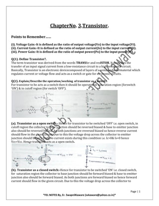
  • 1. Page | 1 *FEL NOTES By, Er. SwapnilKaware (svkaware@yahoo.co.in)* ChapterNo. 3.Transistor. Points to Remember…… (i). Voltage Gain:-It is defined as the ratio of output voltage(Vo) to the input voltage(Vi). (ii). Current Gain:-It is defined as the ratio of output current(Io) to the input current(Ii). (iii). Power Gain:-It is defined as the ratio of output power(Po) to the input power(Pi). Q(1). Define Transistor?. The term transistor was derived from the words TRANSfer and resISTOR. It describes the transfer of an input signal current from a low-resistance circuit to a high resistance circuit. Basically, Transistor is an electronic devicecomposed of layers of a semiconductormaterial which regulates current or voltage flow and acts as a switch or gate for electronic circuits. Q(2). Explain/Describe the operation/working of transistor as a switch?. For transistor to be acts as a switch then it should be operated in saturation region (forswitch ‘ON’) & in cutoff region (for switch ‘OFF’). (a). Transistor as a open switch:- Hence for transistor to be switched ‘OFF’ i.e. open switch, in cutoff region the collector to base junction should be reversed biased & base to emitter junction also should be reversed biased. As both junctions are reversed biased so hence reverse current should flow in the given circuit. Due to this the voltage drop across the collector to emitter junction should be very high.No current exists during this condition i.e. Ic=0& IB=0 hence VcE=Vcc. Hence transistor acts as a open switch. (b). Transistor as a closed switch:-Hence for transistor to be switched ‘ON’ i.e. closed switch, for saturation region the collector to base junction should be forward biased & base to emitter junction also should be forward biased. As both junctions are forward biased so hence forward current should flow in the given circuit. Due to this the voltage drop across the collector to
  • 2. Page | 2 *FEL NOTES By, Er. SwapnilKaware (svkaware@yahoo.co.in)* emitter junction should be very less (i.e. from 0.2V to 1V)& the resulting value of collector current (Ic) becomes very large.Hence transistor acts as a closed switch. Q(3). Explain/Draw Common-Base (CB)configuration of transistor?. In below circuit diagram, The Base terminal is common between input and output hence the given transistor is said to be in CB configuration. In CB configuration, the input is connected between emitter and base terminals and output is taken across collector and base terminals. Also Base terminal is common to both supply voltages i.e. VEB& VCC. As the transistor used is NPN, hence The EB junction is forward biased and CB junction is reverse biased. Hence IE is the input current & IB is the output current. So the current gain (α) or current amplification factor is given by,(α)=IC/IE also IC=(α)*IE. The value (α) is very small i.e. should be equal to 1 (from 0.95 to 0.99). As value of IE deccreses the resulting value of IC also decreases to 0. This current is also called as reverse saturation current ICB at IE=0. Hencewe can also say that, IC=(α) * IE+ICB. Q(4). Drawinput/output characteristics Common-Base (CB)configuration of transistor?. Q(5). Explain/Draw Common-Emitter (CE)configuration of transistor?. In below circuit diagram, Theemitter terminal is common between input and output hence the given transistor is said to be in CE configuration. In CE configuration the input is connected between the base and emitter while output is taken between collector and emitter. Also Emitter terminal is common to both supply voltages i.e. VBE& VCC. As the transistor used is PNP, hence The EB junction is reversed biased and CB junction is also reversed biased (cutoff configuration). So IE&IB should be equals to 0. Hence during this condition the the reverse/leackage/minority current flows called as cutoff current from collector to emitter (ICE) at IB=0.VBE is the input voltage and VCE is output supply at collector.The ratio of change in IC to change in IB is β (DC current gain).
  • 3. Page | 3 *FEL NOTES By, Er. SwapnilKaware (svkaware@yahoo.co.in)* Q(6). Drawinput/output characteristics Common-Emitter (CE)configuration of transistor?. Q(7). Explain/Draw Common-Collector (CC)/Emitter followerconfiguration of transistor?. In below circuit diagram, The Collector terminal is common between input and output hence the given transistor is said to be in CC configuration. The circuit is similar to CE configuration hence also known as emitter follower circuit. In this configuration the relation between IE& IB is given by IE= (1+β)*IB. For operation /working please refer the question no. 5. Q(8). Give the types of amplifiers?. The amplifier can be distinguished depending on which terminal is common to both input & output. They are as follows, (i). Common Emitter (CE) amplifier, (ii). Common Collector (CC) amplifier, (iii). Common Base (CB) amplifier. Q(9). Explain working of transistor as an current amplifier?. Q(10). Describe how amplification takes place in transistor amplifier?. Please refer the question no.5 for answer.
  • 4. Page | 4 *FEL NOTES By, Er. SwapnilKaware (svkaware@yahoo.co.in)* Q(11). Compare/Write differences between CE,CB&CC configurations of transistor amplifiers?. CE Configuration CB Configuration CC Configuration (1). Emitter terminal is common. (1). Base terminal is common. (1). Collector terminal is common. (2). Input resistance is Medium. (2). Input resistance is Low. (2). Input resistance is High. (3). Output resistance is Medium. (3). Output resistance is High. (3). Output resistance is Low. (4). Current gain is High. (4). Current gain is less than 1. (4). Current gain is High. (5). Voltage gain is High. (5). Voltage gain is High. (5). Voltage gain is less than 1. (6). Used as a voltage amplifiers. (6). Used as a low noise amplifiers. (6). Used as a Voltage buffer amplifier. (7). Phase shift between Vi & Vo is 180°. (7). Phase shift between Vi & Vo is 0. (7). Phase shift between Vi & Vo is 0. Q(12). Explain single stage RC coupled CE amplifier?OR Q(13). Explain/Draw CE amplifier & also state its working? OR Q(14). Explain single stage CE amplifier using NPN transistor ?.OR Q(15). Explain the function of each component of RC amplifier?. The diagram for single stage RC coupled amplifier is as shown in above figure. Construction:-In above circuit the transistor is connected in CE configuration hence we called it as CE amplifier. As seen from the above diagram, The above circuit contains NPN transistor,the capacitors C1 & C2 are coupling capacitors,CE is the emitter bypass capacitor, RE is the emitter resistance. R1 & R2 are biasing resistors, there is load resistor also known as collector resistance (RC) is present.In above circuit the load resistance (Rc) is coupled/grouped with coupling capacitors C1 & C2 hence we called it as RC coupled amplifier. Working:-For transistor to be acts as an amplifier it is required that transistor should operate in the active region. Hence we have used resistors R1,R2& RE for biasing/connecting the transistor in active region.Rc is the collector resistor used for controlling collector current. We have used the capacitor C1 for coupling AC voltage input (Vi) to the base of the transistor. This capacitor
  • 5. Page | 5 *FEL NOTES By, Er. SwapnilKaware (svkaware@yahoo.co.in)* (C1) blocks any DC component present in AC input voltage (Vi) and only couples AC components of the input signal. The capacitor which is connected in parallel with emitter resistance RE is known as emitter bypass capacitor (CE).the value of RE should be as small as possible for better AC voltage gain & it should be very high as possible for better stability.CE terminal acts as open circuit for DC component i.e. CE will not allows any DC component to flow. Also CE acts as a closed circuit for AC component i.e. CE will allow any AC component to flow & bypasses RE for only AC signals. Hence it will increase the voltage gain of amplifier. The coupling capacitor C2 couples the amplifier output to the load resistance or to the next stage of amplifier. Also it passes AC part of amplified signal to the load. Finally the collector voltage is given by VC=VCC-IC*RC. This collector voltage is then coupled/connected to the load through coupling capacitor C2. Then C2 amplifies this voltage & removes DC component from it. So finally we gets amplified AC signal at the output. The shape of this signal is exactly same as input signal but its magnitude is much higher than that of input signal (Vi). Finally we can observe that there is a 180° phase shift between Vi & Vo. Q(16). Explain single stage RC coupled CB amplifier?OR Q(17). Explain/Draw CB amplifier & also state its working? OR Q(18). Explain single stage CB amplifier using NPN transistor ?. Please refer the question no. 11,12,13& 14 for construction & working. Q(19). Draw frequency response characteristics of single stage RC coupled amplifier?.OR Q(20). Explain frequency response curve & bandwidth of RC coupled amplifier?.OR Q(21). Explain the terms: (a). Lower Cutoff Frequency, (b). Higher Cutoff Frequency?.ORQ(22). Define the terms:- (c). Bandwidth, (d).Half Power Point.
  • 6. Page | 6 *FEL NOTES By, Er. SwapnilKaware (svkaware@yahoo.co.in)* As seen from the above frequency response of RC coupled amplifier, the above curve shows how the magnitude of voltage gain (AV)of amplifier changes with the frequency (f) of the input signal.Av (max) is the high voltage gain while Av(max)/√2 is the lower voltage gain which is near about 70.7% of the maximum voltage gain.For the limited band of frequency the gain is constant known as ‘mid band gain’& the corresponding range of frequency is known as ‘mid frequency range’. When the values of frequencies are very high & very low then the gain of amplifier reduces to almost zero value. (a). LowerCutoffFrequency:-f1represents the lower cutoff frequency which is always lesser than f2. f1is the frequency of the input signal at which gain of amplifier reduces to 70.7% of their ‘mid frequency range’ value. (b).HigherCutoffFrequency:-f2 represents the upper cutoff frequency which is always higher than f1.f2 is the frequency of the input signal at which gain of amplifier reduces to 70.7% of their ‘mid frequency range’ value. (c). Bandwidth (B.W.):- It is defined as the difference between upper cutoff frequency (f2) & lower cutoff frequency (f1). So, B.W.= f2-f1. (d). HalfPowerPoint:-The point or region formed by frequencies f1 & f2 known as half power point. (Region represented by Av(max)/√2 ). Q(23). State/Give the different types of coupling amplifiers?.OR Q(24). Classify amplifiers based on the type of coupling used?. (a). RC coupling,(b). Transformer coupling,(c).Direct coupling. Q(25). Draw & explain the circuit of two stage (multi stage)RC coupled amplifier?. Q(26). Draw & explain frequency response curve/characteristics of two stage RC coupled amplifier?. Please refer the question no. from 16 up to 22 for explanation. Q(27). Give advantages of RC coupled amplifiers?. (a). Bandwidth is larger,(b). Coupling is efficient for better results. (c). Noise level is lesser.(d). Coupling is less expensive. Q(28). Give applications of RC coupled amplifiers?. (a). TV,VCR,CD,DVD players.(b). Tape recorders.
  • 7. Page | 7 *FEL NOTES By, Er. SwapnilKaware (svkaware@yahoo.co.in)* Q(29). Draw the circuit of transformer coupled amplifier?. Q(30). Draw frequency response curve/characteristics of transformer coupled amplifier?. In above circuit the given transformer can not transfer DC components from primary side coil towards secondary side coil. Hence it will not allow any DC component to flow from output of first stage to the input of next stage transistor amplifier. Q(31). Draw & explain working of direct coupled (DC) amplifier?. Q(32). Draw frequency response curve/characteristics of direct coupled (DC) amplifier?. As seen from the above diagram both transistors Q1 & Q2 are direct coupled with their signals each other. In this output signal of first stage amplifier is directly connected to the input of second stage amplifier without help of any component. This type of biasing allows the collector current to pass through the next stage amplifier thereby affecting its biasing conditions. Hence whatever be the changes occurred in second stage amplifier will affects signal conditions of first stage amplifier due to direct coupling. This problem of such amplifiers is known as ‘DRIFT’. In case of ‘DRIFT’ problem both DC & AC voltages are coupled from first stage to second stage.That means DC signal is alsoamplified in this model hence it is called as DC (direct coupled) amplifier. The frequency response of such amplifier is lower but better because of absence of coupling capacitors.
  • 8. Page | 8 *FEL NOTES By, Er. SwapnilKaware (svkaware@yahoo.co.in)* Q(33). Draw & explain working of 3-stage direct coupled (DC) amplifier?. Q(34). Draw frequency response curve/characteristics of 3-stage direct coupled (DC) amplifier?. Please refer the question no. 31 & 32 for working. Q(35). Compare/Write differences between RC coupled, Transformer coupled & Direct coupled (DC) amplifiers?. RC coupled Transformer coupled Direct coupled (DC) (1). Coupling components used are resistors & capacitors. (1). Coupling component used is transformer. (1). No coupling components are used. (2). Only AC signal can be coupled. (2). Only AC signal can be coupled. (2). Both AC & DC signals can be coupled. (3). DC amplification is not possible. (3). DC amplification is not possible. (3). DC amplification is possible. (4). ‘Drift’ problem is absent. (4). ‘Drift’ problem is absent. (4). ‘Drift’ problem is present. (5). Frequency response is good. (5). Frequency response is poor. (5). Frequency response is best. (6). Cost is small. (6). Cost is very high. (6). Cost is very small. (7). Used in radios & TV. (7). Used in power amplifiers. (7). Used in DC amplification devices. Q(36). Explain the classification of power amplifiers?. Depending on the location of Q-point or operating on the load line, the power amplifiers can be classified as follows, (1). Class-A amplifier,(2). Class-B amplifier,(3). Class-C amplifier,(4). Class-AB amplifier. Sr. No. Type of Amplifier Location of Q Point 1. Class-A amplifier At the center of load line. 2. Class-B amplifier In the cutoff region. 3. Class-C amplifier Below the cutoff region. 4. Class-AB amplifier Just above the cutoff region.
  • 9. Page | 9 *FEL NOTES By, Er. SwapnilKaware (svkaware@yahoo.co.in)* Q(37). Draw input & output waveforms of Class-A amplifier?. Q(38). Draw input & output waveforms of Class-B amplifier?. Q(39). Draw input & output waveforms of Class-C amplifier?.
  • 10. Page | 10 *FEL NOTES By, Er. SwapnilKaware (svkaware@yahoo.co.in)* Q(40). Draw input & output waveforms of Class-AB amplifier?. Q(41). Compare/Write differences between class A, class B, class C & class AB amplifiers?. Class-A Class-B Class-C Class-AB (1). Efficiency is between 25% to 50%. (1). Efficiency is 78.5% (1). Efficiency is 95% (1). Efficiency is between 50% to 78.5%. (2). Power dissipation is very high. (2). Power dissipation is low. (2). Power dissipation is very low. (2). Power dissipation is medium. (3). No distortion in output. (3). Distortion in output is more than class A. (3). Distortion in output is more than A, B & AB. (3). Distortion in output is low. (4). Location of operating point is at the center of load line. (4). Location of operating point is on the X axis of load line. (4). Location of operating point is below the X axis of load line. (4). Location of operating point is above the X axis but below the midpointof load line. (5). Conduction angle of collector current is 360°. (5). Conduction angle of collector current is 180°. (5). Conduction angle of collector current is less than 180°. (5). Conduction angle of collector current is between 180° & 360°. (6). Used as a voltage amplifier. (6). Used as a radio amplifier. (6). Used in music systems. (6). Used in transmitters. (7). Diagram. (7). Diagram. (7). Diagram. (7). Diagram. Q(42). Define feedback also give its types?. Feedback:-It is defined as the process in which part output signal is returned back to the input signal. There are two types of feedback, (a). Positive Feedback:- It is defined as the feedback process in which original input signal is in phase with feedback signal. Such type of feedbacks is used in oscillators. (b). Negative Feedback:- It is defined as the feedback process in which original input signal is not in phase with feedback signal. Such type of feedbacks is used in amplifiers.
  • 11. Page | 11 *FEL NOTES By, Er. SwapnilKaware (svkaware@yahoo.co.in)* Q(43). State advantages of negative feedback amplifier?. (1). Better stability,(2).Operating point is regulated. (3). Frequency response is better,(4).Drift problem is less, (5). Less distortion (noise),(6). Increasing input resistance, (7). Decreasing output resistance,(8). Bandwidth is better. Q(44). Define Oscillator&give its classification?. Oscillator:-They are derived from the term ‘amplifier’ by which they does not have any AC input signal that means noise voltage which is generated by random movement of electrons inside any electronic device is amplified by the amplifier which becomes the input voltage for the oscillators, but they operates on the principle of positive feedback for generating AC output signal. Oscillators produce repetitive sine waves, square waves or even saw tooth waves. Oscillator converts DC signal from power supply to AC signal. Hence oscillators can be thought as an amplifier which produces its own input signal. The classification of oscillators is as shown in below diagram, Oscillators RC Oscillators. LC Oscillators (i). Phase shift oscillator, (i).Hartley oscillator (ii). Wein Bridge oscillator. (ii). Colpitt’s oscillator (iii). Crystal oscillator Q(45). Explain Barkhausen’s criterion for oscillators?. For amplifiers to be worked as an oscillators they should satisfy ‘Barkhausen’s criterion’. (a). Figure showing phase shift around the loop. (b). Fig. showing loop gain Aβ>=1. The frequency for which a sinusoidal waveform oscillator will operate is the frequency for which the total phase shift introduced, as a signal proceeds from the input terminals through the amplifier and feedback network, and back to the input is preciselyzero ( or of course an integral multiple of 2π). That is the frequency of a sinusoidal oscillator is determined by the condition thatthe loop gain phase shift is zero.The overall gain of the feedback amplifier is given by, Avf=Av/(1-Av*β),also Avf=Vo/Vi, Where Av is the loop gain of the amplifier &βis the feedback factor (portion of output voltage given back to the input).
  • 12. Page | 12 *FEL NOTES By, Er. SwapnilKaware (svkaware@yahoo.co.in)* Hence for overall gain of the amplifier (Avf) to be larger it is required that, the product Av*βshould be positive, i.e. they should be in phase with each other so that their product becomes positive. & finally the factor (1-Av*β) becomes less than unity for producing better amplifier gain.Hence Avβ>=1. This criterion is known as ‘Barkhausen criterion’ for oscillations. Q(46). Draw the circuit diagram for RC phase shift oscillator & describe its working? Q(47). Give the formula for frequency of oscillation for RC phase shift oscillator ?. As seen from the above diagram, the given circuit contains three capacitors & three resistors connected in parallel with each other. Each RC network is designed to give phase shift of 60°. Hence due to three identical RC networks the above circuit gives phase shift of 180° for only same frequency.So, For producing phase shift of 180°we have to use the same/identical values for resistor (R) & capacitor (C).When a sinusoidal voltage (Vi=e0*sinώt) of frequency f=ώ/2ᴨ.is applied to the give RC phase shift oscillator circuit. The output voltage leads the input voltage by 180° which is given by formula, tan φ=1/(ώ*R*C), but ώ=2ᴨf, therefore, tan φ=1/(2ᴨ*f*R*C). Where φis the phase angle, therefore,φ =tan¯¹ (1/(2ᴨ*f*R*C)).But, tan 60°=√3. Hence frequency for the oscillation is given by, f=1/(2ᴨ*R*C*√3). Q(48). Draw the circuit diagram for RC phase shift oscillator with transistor & describe its working? For working please refer the question no. 46 & 47. In above given circuit RL is the load resistance, while transistor used is of NPN type in common emitter (CE) configuration. R1 & R2 are the biasing resistors. This circuit also produces phase shift of 180° & also the given NPN type transistor produces the phase shift of 180°, hence total phase shift produced by above circuit is 360° in common emitter (CE) configuration.
  • 13. Page | 13 *FEL NOTES By, Er. SwapnilKaware (svkaware@yahoo.co.in)* Q(49). Give the advantages/applications of phase shift oscillator?. (i). Construction is simple.(ii). Suitable for wide frequency range applications. (iii). Used for audio frequency oscillations.(iv). Output signal produce is better. (v). Used in signal generators. Q(50). Draw the circuit diagram for Hartley oscillator & describe its working? Q(51). Draw the circuit diagram for Hartley oscillator & describes how it satisfies‘Barkhausen’s criterion’? Q(52). Give the formula for frequency of oscillations for Hartley oscillator? The Hartley oscillator using NPN transistor is shown in above figure.The above circuit contains capacitor CT& two transformer coils L1 & L2 inductively coupled with each other. RB is the biasing resistor connected in between base & collector terminal. The above circuit is connected in CE configuration hence it gives 180° phase shift between input & output.The components L1,L2& CT formed the feedback circuit (tank circuit) which gives additional 180° phase shift for positive feedback. Hence by this way this circuit satisfies ‘Barkhausen’s criterion’.After the application of power supply as soon as the switch is closed then the collector current starts increasing and charges the capacitor CT. After fully charging the capacitor CT, then it dischargesthrough inductors L1 and L2 setting up oscillations. These oscillations across L1 are appliedto the base-emitter junction and appear in the amplified form at the collector.The coil L2 couples collector circuit energy back by means of mutual inductionbetween L1 and L2. In this way, energy is continuously supplied back to the tank (L1-L2-C1) circuit to overcome the losses in it. Consequently continues un-dampedoscillations will obtain.Thefrequency of oscillations (F) of the circuit is given by, F= 1/(2ᴨ*√(CT(L1+L2)). Q(53). Give the advantages/applications of Hartley oscillator?. (i). Used function generators,(ii). Used in radio frequency applications. (iii). Used in TV receivers. Q(54). Draw the circuit diagram for Colpitt’s oscillator & describe its working?. Q(55). Draw the circuit diagram for Colpitt’s oscillator & describes how it satisfies ‘Barkhausen’scriterion’?. Q(56). Give the formula for frequency of oscillations for Colpitt’s oscillator?.
  • 14. Page | 14 *FEL NOTES By, Er. SwapnilKaware (svkaware@yahoo.co.in)* The Colpitt’s oscillator using NPN transistor is shown in above figure.In this two capacitors are placed across a common inductor as shown below so that C1, C2 and L2forms the feedback (tank) circuit. RB is the biasing resistor connected in between base & collector terminal. When the power supply is turned on, C1 and C2 get charged .These capacitors then discharge through the coil L2 & L3, setting up oscillations whose frequency depends on the values of L2,L3, C1,and C2.The oscillations across C1 are applied to the Base-Emitter junction and appear in the amplified form in the collector circuit. The amount of feedback depends on the values of C1 and C2. Smaller the C1 the greater will be the feedback .The capacitors C1 and C2 act as a simple voltage divider. The above circuit is connected in CE configuration hence it gives 180° phase shift between input & output.The components L2,L3& CT formed the feedback circuit (tank circuit) which gives additional 180° phase shift for positive feedback. Hence by this way this circuit satisfies Barkhausen’s criterion.Thefrequency of oscillations (F) of the circuit is given by. F= 1/(2ᴨ*√(L3+C)).where C=(C1*C2)/(C1+C2). Q(57). Draw the circuit diagram for Crystal oscillator & describe its working? Q(58). Draw the circuit diagram for Crystal oscillator & describes how it satisfies Barkhausen’s criterion? Q(59). Give the formula for frequency of oscillations for Crystal oscillator? (a).Fig.Crystal mounting, (b).Fig.Equivalent circuit. The required circuit diagram for the crystal oscillator is as shown in above figure. In above circuit we have used the quartz crystal for getting better accuracy & stability of the oscillators frequency. Quartz crystals are used because they are readily available & also inexpensive. For operation of circuit, the crystal is to be cut suitably & then placed in between metallic plates as shown in above figure.The amount of current that can safely pass through a crystal ranges from 50mA to 200mA.
  • 15. Page | 15 *FEL NOTES By, Er. SwapnilKaware (svkaware@yahoo.co.in)* When the rated current is exceeded, the amplitude of mechanical vibration becomes too great, and thecrystal may crack. Overloading the crystal affects the frequency of vibration because the powerdissipation and crystal temperature increase with the amount of load current.The circuit contains parallel capacitor (Cp) & series capacitor (Cs) along with resistor (R) & inductor (L). The components R,L& C together forms a resonant circuit. The formula for series resonant frequency is given by,Fs=1/(2ᴨ*√LCs). The formula for parallel resonant frequency is given by,Fp=1/(2ᴨ*√LCp). Q(60). Give the advantages/applications of Crystal oscillator?. (i). Used function generators,(ii). Used in radio frequency applications. (iii). Used in TV receivers. Q(61). Compare Hartley &Colpitt’s oscillator?. Hartley oscillator Colpitt’s oscillator (i).Stability is less. (i). Stability is greater. (ii). No use of crystals. (ii). Crystal controlled. (iii). Cost is high. (iii). Cost is less. (iv). Construction is complex. (iv). Construction is simpler. (v). Efficiency is good. (v). Efficiency is better. (vi). Suitable for medium frequency range. (vi). Suitable for higher frequency range. (vii).Circuit diagram. (vii). Circuit diagram. (viii). Formula for frequency. (viii). Formula for frequency. (ix). Applications. (ix). Applications. *********************************************** ALL THE BEST ***************************************