Downloaded 34 times


![8-bit data from Even address Bank
A 1 - A 1 9
D 0 - D 1 5
B H E = 1
D 8 - D 1 5 D 0 - D 7
x
x + 2
x + 4
A 0 = 0
x + 1
x + 3
x + 5
O d d B a n k E v e n B a n k
MOV SI,4000H
MOV AL,[SI+2]](https://image.slidesharecdn.com/upi2010d028086architecture-141203231724-conversion-gate01/85/8086-architecture-21-320.jpg)
![8-bit Data from Odd Address Bank
A 1 - A 1 9
D 0 - D 1 5
x
x + 2
O d d B a n k E v e n B a n k
x + 1
x + 3
B H E = 0 A 0 = 1
D 8 - D 1 5
D 0 - D 7
MOV SI,4000H
MOV AL,[SI+3]](https://image.slidesharecdn.com/upi2010d028086architecture-141203231724-conversion-gate01/85/8086-architecture-22-320.jpg)
![16-bit Data Access starting from Even Address
A 1 - A 1 9
D 0 - D 1 5
O d d B a n k E v e n B a n k
B H E = 0
x
x + 2
A 0 = 0
x + 1
x + 3
D 8 - D 1 5
D 0 - D 7
MOV SI,4000H
MOV AX,[SI+2]](https://image.slidesharecdn.com/upi2010d028086architecture-141203231724-conversion-gate01/85/8086-architecture-23-320.jpg)
![16-bit Data Access starting from Odd Address
A 1 - A 1 9
O d d B a n k E v e n B a n k
D 8 - D 1 5
D 0 - D 7
A 1 - A 9
0 0 0 5
0 0 0 7
0 0 0 9
0 0 0 4
0 0 0 6
0 0 0 8
A 1 - A 1 9
O d d B a n k E v e n B a n k
D 8 - D 1 5
D 0 - D 7
A 1 - A 9
0 0 0 5
0 0 0 7
0 0 0 9
0 0 0 4
0 0 0 6
0 0 0 8
( a ) F ir s t A c c e s s fr o m O d d A d d re s s ( b ) N e x t A c c e s s fr o m E v e n A d d r e s s
MOV SI,4000H
MOV AX,[SI+5]](https://image.slidesharecdn.com/upi2010d028086architecture-141203231724-conversion-gate01/85/8086-architecture-24-320.jpg)


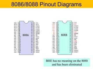
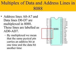
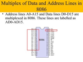
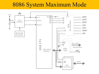
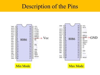
The document discusses the 8086/8088 microprocessors. It describes their basic features, including being 16-bit microprocessors introduced in 1978/1979 and using HMOS technology. It also covers their pin configurations and diagrams, addressing modes, minimum and maximum modes, and descriptions of the various pins and signals.


![[Advantech] Modbus protocol training (ModbusTCP, ModbusRTU)](https://cdn.slidesharecdn.com/ss_thumbnails/modbustraining-161115125830-thumbnail.jpg?width=640&height=640&fit=bounds)