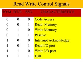
![8-bit data from Even address Bank
O dd B an k E ven B a n k
x + 1 x
x + 3 x + 2
x + 5 x + 4
B H E = 1 A 0 = 0
D 8 -D 1 5 D 0 -D 7
A 1 -A 1 9
D 0 -D 1 5
MOV SI,4000H
MOV AL,[SI+2]](https://image.slidesharecdn.com/8086architecture-121118095725-phpapp02/85/8086-architecture-21-320.jpg)
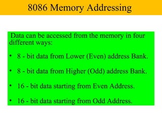
![8-bit Data from Odd Address Bank
O dd B ank Even Bank
x + 1 x
x + 3 x + 2
BH E =0 A0 = 1
A 1 -A 1 9
D 0 -D 7
D 8 -D 1 5
D 0 -D 1 5
MOV SI,4000H
MOV AL,[SI+3]](https://image.slidesharecdn.com/8086architecture-121118095725-phpapp02/85/8086-architecture-22-320.jpg)
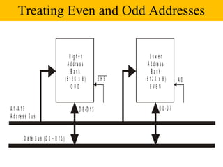
![16-bit Data Access starting from Even Address
O dd B ank Even Bank
x + 1 x
x + 3 x + 2
A0 = 0
BHE =0
A 1 -A 1 9 D 8 -D 1 5
D 0 -D 7
D 0 -D 1 5
MOV SI,4000H
MOV AX,[SI+2]](https://image.slidesharecdn.com/8086architecture-121118095725-phpapp02/85/8086-architecture-23-320.jpg)
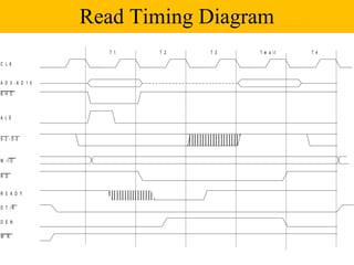
![16-bit Data Access starting from Odd Address
O dd B ank Even Bank O dd B ank Even Bank
0005 0004 0005 0004
0007 0006 0007 0006
0009 0008 0009 0008
A 1 -A 1 9 A 1 -A 1 9
A 1 -A 9 A 1 -A 9
D 0 -D 7 D 0 -D 7
D 8 -D 1 5 D 8 -D 1 5
( a ) F ir s t A c c e s s f r o m O d d A d d r e s s (b ) N e x t A c c e s s fro m E v e n A d d re s s
MOV SI,4000H
MOV AX,[SI+5]](https://image.slidesharecdn.com/8086architecture-121118095725-phpapp02/85/8086-architecture-24-320.jpg)

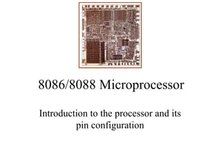
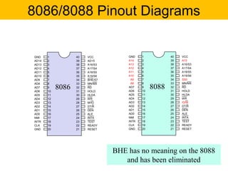
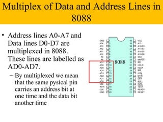
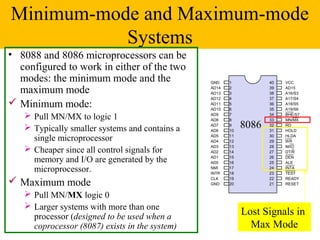
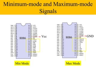
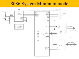
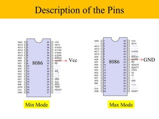
The document discusses the 8086/8088 microprocessors. It introduces their basic features, including being 16-bit processors manufactured using HMOS technology. It provides pinout diagrams showing the 40-pin package and labeling of the pins. It describes the 8088 having an 8-bit data bus while the 8086 has a 16-bit data bus. It also explains the minimum and maximum modes the processors can operate in.