Downloaded 427 times

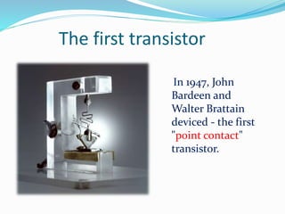
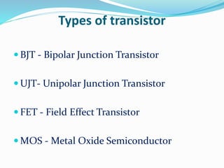
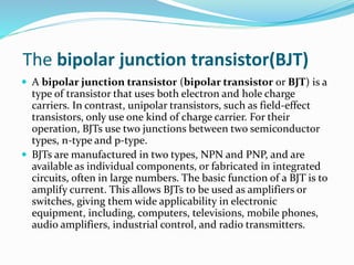
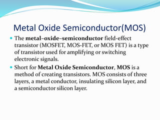
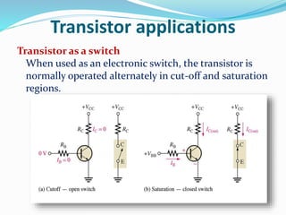
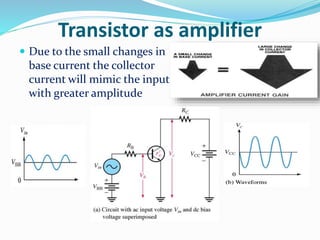
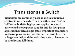


The document discusses transistors, including: - Transistors are electronic devices made of three layers of semiconductor material that can act as insulators or conductors. - The first transistor was invented in 1947 by John Bardeen and Walter Brattain. - There are several types of transistors including BJT, UJT, FET, and MOS transistors. BJTs use both electrons and holes, while FETs use only one type of carrier. - Transistors have wide applications as switches, amplifiers, and in digital circuits. Recent developments include 3D transistors made using tri-gate technology for improved performance and efficiency.


