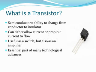
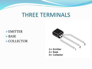
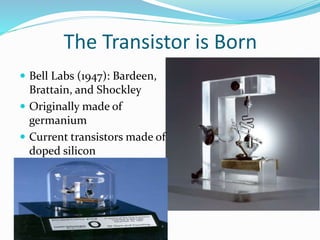
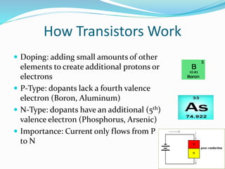
KRCT
What is a Transistor?
 Semiconductors: ability to change from
conductor to insulator
 Can either allow current or prohibit
current to flow
 Useful as a switch, but also as an
amplifier
 Essential part of many technological
advances
THREE TERMINALS
EMITTER
BASE
COLLECTOR
The Transistor is Born
 Bell Labs (1947): Bardeen,
Brattain, and Shockley
 Originally made of
germanium
 Current transistors made of
doped silicon
Nobel prize
William Shockley ,Walter Brattain ,John Bardeen
How Transistors Work
 Doping: adding small amounts of other
elements to create additional protons or
electrons
 P-Type: dopants lack a fourth valence
electron (Boron, Aluminum)
 N-Type: dopants have an additional (5th)
valence electron (Phosphorus, Arsenic)
 Importance: Current only flows from P
to N
DOPING
 The addition of a small amount
of a different substance to a
pure semiconductor crystal.
 The impurities give an excess of
conducting electrons or an
excess of conducting holes
which is crucial for making a
working transistor.
TYPES OF TRANSISTOR
 Bipolar Junction Transistor (BJT)
 Field-Effect Transistor (FET)
 Junction Field Effect Transistor (JFET)
 Metal Oxide Semiconductor Field Effect Transistor
(MOSFET)
Junction Field Effect Transistor
(JFET)
 The field-effect transistor
(FET) controls the current
between two points but
does so differently than the
bipolar transistor.
 The FET operates by the
effects of an electric field.
 This is why the FET is
sometimes called a
unipolar transistor.
JFET Properties
 Cut-off voltage is varying
for each JFET0.3V – 10V
 N-Channel – Negative
VGS
 P-Channel – Positive VGS
Internal Capacitance
 Do not Forward Bias
JFET – burn out
Metal oxide semiconductor field effect
transistor(MOSFET)
The most common field effect transistor in both
digital and analog circuits.
Uses channel of n or p-type semiconductor,
named NMOSFET and PMOSFET, respectively.
SILICON ON INSULATOR (SOI)
 For high-frequency circuits
(about 5 GHz) capacitive
coupling to the Si substrate
limits the switching
frequency.
 These problems are being
avoided by making circuits
on insulating substrates
that have a thin,
approximately 100 nm
layer of crystalline silicon
APPLICATION
 In integrated circuits, the desirable properties of
MOSFETs allowed them to capture nearly all market
share for digital circuits.
 Discrete MOSFETs can be applied in transistor
applications, including analog circuit.
MEDICAL APPLICATION
 There is great interest in
constructing nano electronic
devices that could detect the
concentrations of bio molecules
 A parallel line of research seeks
to create nano electronic devices
which could interact with single
cells for use in basic biological
research.
 These devices are called nano
sensors.
NANO MEDICINE
USING IN COMPUTER
Transistors have continued to get smaller and
smaller.
For instance, each memory location in a
computer has a pair of transistors, and there are 16
of them for each byte of memory.
COMPUTER MEMORY
Normally, a junction transistor is "off" when there is no
base current and switches to "on" when the base current
flows. That means it takes an electric current to switch
the transistor on or off.
This kind of arrangement is known as a flip-flop
ADVANTAGE & LIMITATION
ADVANTAGE;
Lower power dissipation and generally greater energy
efficiency.
Low operating voltages compatible with batteries of
only a few cells
LIMITATION;
Silicon transistors can age and fail
Sensitivity to radiation and cosmic rays
Transistor history and types

Transistor history and types

  • 2.
  • 4.
    What is aTransistor?  Semiconductors: ability to change from conductor to insulator  Can either allow current or prohibit current to flow  Useful as a switch, but also as an amplifier  Essential part of many technological advances
  • 5.
  • 6.
    The Transistor isBorn  Bell Labs (1947): Bardeen, Brattain, and Shockley  Originally made of germanium  Current transistors made of doped silicon
  • 7.
    Nobel prize William Shockley,Walter Brattain ,John Bardeen
  • 8.
    How Transistors Work Doping: adding small amounts of other elements to create additional protons or electrons  P-Type: dopants lack a fourth valence electron (Boron, Aluminum)  N-Type: dopants have an additional (5th) valence electron (Phosphorus, Arsenic)  Importance: Current only flows from P to N
  • 9.
    DOPING  The additionof a small amount of a different substance to a pure semiconductor crystal.  The impurities give an excess of conducting electrons or an excess of conducting holes which is crucial for making a working transistor.
  • 10.
    TYPES OF TRANSISTOR Bipolar Junction Transistor (BJT)  Field-Effect Transistor (FET)  Junction Field Effect Transistor (JFET)  Metal Oxide Semiconductor Field Effect Transistor (MOSFET)
  • 11.
    Junction Field EffectTransistor (JFET)  The field-effect transistor (FET) controls the current between two points but does so differently than the bipolar transistor.  The FET operates by the effects of an electric field.  This is why the FET is sometimes called a unipolar transistor.
  • 12.
    JFET Properties  Cut-offvoltage is varying for each JFET0.3V – 10V  N-Channel – Negative VGS  P-Channel – Positive VGS Internal Capacitance  Do not Forward Bias JFET – burn out
  • 13.
    Metal oxide semiconductorfield effect transistor(MOSFET) The most common field effect transistor in both digital and analog circuits. Uses channel of n or p-type semiconductor, named NMOSFET and PMOSFET, respectively.
  • 14.
    SILICON ON INSULATOR(SOI)  For high-frequency circuits (about 5 GHz) capacitive coupling to the Si substrate limits the switching frequency.  These problems are being avoided by making circuits on insulating substrates that have a thin, approximately 100 nm layer of crystalline silicon
  • 15.
    APPLICATION  In integratedcircuits, the desirable properties of MOSFETs allowed them to capture nearly all market share for digital circuits.  Discrete MOSFETs can be applied in transistor applications, including analog circuit.
  • 16.
    MEDICAL APPLICATION  Thereis great interest in constructing nano electronic devices that could detect the concentrations of bio molecules  A parallel line of research seeks to create nano electronic devices which could interact with single cells for use in basic biological research.  These devices are called nano sensors.
  • 17.
  • 20.
    USING IN COMPUTER Transistorshave continued to get smaller and smaller. For instance, each memory location in a computer has a pair of transistors, and there are 16 of them for each byte of memory.
  • 21.
    COMPUTER MEMORY Normally, ajunction transistor is "off" when there is no base current and switches to "on" when the base current flows. That means it takes an electric current to switch the transistor on or off. This kind of arrangement is known as a flip-flop
  • 22.
    ADVANTAGE & LIMITATION ADVANTAGE; Lowerpower dissipation and generally greater energy efficiency. Low operating voltages compatible with batteries of only a few cells LIMITATION; Silicon transistors can age and fail Sensitivity to radiation and cosmic rays

Editor's Notes