The document discusses micromachining, which refers to machining processes that remove small amounts of material to achieve high geometric accuracy at the micro level. Key points include:
- Micromachining is used to manufacture micro-structures and parts 1-500 micrometers in size.
- There is a growing demand for miniaturized products, driving increased use of micromachining.
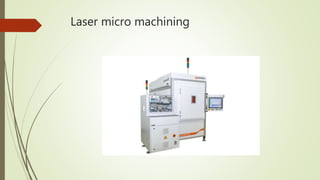
- Micromachining techniques include bulk micromachining, surface micromachining, LIGA, and laser micromachining.
- Micromachining has applications in fields like biotechnology, medical devices, optics, and sensors.