Download to read offline

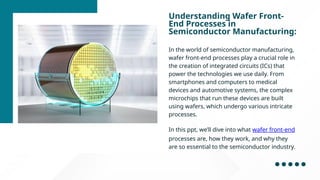

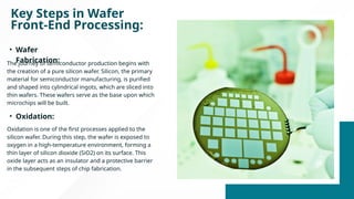

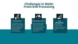


Wafer front-end processing is a vital stage in semiconductor manufacturing that transforms raw silicon wafers into functioning microchips through various intricate processes. Key steps include wafer fabrication, oxidation, photolithography, and etching, all of which must occur in cleanroom environments to avoid contamination. The document also discusses challenges such as miniaturization, contamination control, and yield management in the production process.