Download to read offline

![M Singh Sankhwar et al Int. Journal of Engineering Research and Applications
ISSN : 2248-9622, Vol. 4, Issue 1( Version 2), January 2014, pp.152-159
www.ijera.com
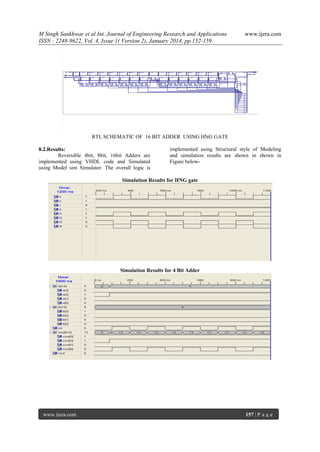
Simulation Results for 8 Bit Adder
Simulation Results for 16 bit Adder
IX.
Conclusion
The Reversible HNG gate are used to
implement Adders . In this paper, we proposed
Reversible 4bit, 8bit,16 bit Parallel Binary Adder
unit. , these can be used for low power applications.
In future, the design can be extended to any number
of bits for Parallel Binary Adder unit and also for low
power Reversible ALUs, Multipliers and Dividers.
References
[1]
[2]
[3]
[4]
R. Landauer, "Irreversibility and Heat
Generation in the Computational Process",
IBM Journal of Research Development, 5,
1961, 183-191.
Bennett, C., "Logical Reversibility of
Computation," IBM Journal of Research
and Development, 17, 1973, 525-532.
Hafiz Md. Hasan Babu and A. R.
Chowdhury, "Design of a Reversible Binary
Coded Decimal Adder by Using Reversible
4-bit Parallel Adder", VLSI Design 2005,
pp-255-260, Kolkata, India, Jan 2005.
Himanshu. Thapliyal, S. Kotiyal and M.B
Srinivas, "Novel BCD Adders and their
Reversible Logic Implementation for IEEE
754r Format", VLSI Design 2006,
Hyderabad, India, Jan 4-7, 2006, pp. 387392.
www.ijera.com
[5]
R. James, T. K. Shahana, K. P. Jacob and S.
Sasi,"Improved
Reversible
Logic
Implementation of Decimal Adder", IEEE
11th VDAT Symposium Aug 8-11, 2007.
[6]
Md. M. H. Azad Khan, "Design of Fulladder
With
Reversible
Gates",
InternationalConference on Computer and
Information Technology, Bangladesh, 2002,
pp. 515-519.
[7]
R. Feynman, "Quantum Mechanical
Computers", Optical News, 1985, pp. 11-20.
[8]
H. Thapliyal and M.B Srinivas, "A Novel
Reversible TSG Gate and Its Application
forDesigning Reversible Carry Look-Ahead
and Other Adder Architectures", Tenth AsiaPacific Computer Systems Architecture
Conference, Singapore, Oct 24 - 26, 2005
[9]
Rekha K.james,Shahana T.K,T.Poulose
Jacob,Sreela Sasi “A new look at Reversible
logic
implementation
of
Decimal
adder”,IEEE 1- 4244-1368-0/07.
[10] Jagadguru Swami Sri Bharati Krishna
Tirthaji Maharaja, Vedic Mathematics:
Sixteen Simple Mathematical Formulae from
the Veda, Delhi (1965).
[11] Rakshith Saligram and Rakshith T.R.
"Novel
Code
Converter
Employing
Reversible Logic", International Journal of
158 | P a g e](https://image.slidesharecdn.com/s4102152159-140130012312-phpapp02/85/S4102152159-7-320.jpg)
![M Singh Sankhwar et al Int. Journal of Engineering Research and Applications
ISSN : 2248-9622, Vol. 4, Issue 1( Version 2), January 2014, pp.152-159
Computer
2012.
Applications
(IJCA),
www.ijera.com
August
[12] Himanshu. Thapliyal ,K.p Jacob, Majid
haghparast & Keivan Navi Design of High
speed low power Reversible Logic BCD
Adder Using HNG gate IEEE Transactions
on VLSI Systems,March 2013.
ABOUT THE AUTHORS
Manjeet Singh Sankhwar has 3 years
of Teaching experience and presently pursuing
MTech in Micro Electronics & VLSI Design in
SGSITS Indore, India .He received his Bachelor of
Engineering in Electronics and Communication from
UIT-RGPV Bhopal,India in 2008 . His main research
interests include Low Power VLSI design, Digital
design.
Mr. Rajesh Khatri has 20 years of
Teaching experience and presently working as
Associate Professor in Department of Electronics &
Instrumentation Engineering at SGSITS Indore. He
received his Bachelor of Engineering in Electronics
and Communication from SGGS Institute of
Technology Nanded, India in 1990. He received his
Master of Engineering in Instrumentation from
SGGS Institute of Technology Nanded, India in
1995.
www.ijera.com
159 | P a g e](https://image.slidesharecdn.com/s4102152159-140130012312-phpapp02/85/S4102152159-8-320.jpg)

This research article presents a new design for a high-speed, low-power reversible logic adder using HNG gates, aiming to minimize energy dissipation through reversible computing principles. The proposed implementation reduces the number of gate operations and garbage outputs compared to existing designs, making it suitable for applications in nanotechnology. The findings suggest that this design can be extended for larger parallel binary adder units and other low-power circuits.