In the digital circuit design, the primary factors are low power and a high packing density. The reversible logic circuit in quantum-dot cellular
automata (QCA) framework is hoped to be effective in addressing the factor of power consumption at nanoscale regime. Fault tolerant circuits are suited of interruption of errors at the outputs. This manuscript focuses the design of ALU in QCA-based and propose new parity preserving gate. It has been introduced that new reversible gate, namely, universal parity preserving gate (UPPG), to
optimise the ALU circuits. An algorithm and lemmas are shown in designing ALU. The ALU generates a number of arithmetic and logical function with using only less architectural complexity. Most importantly circuit design
focuses on optimising the gate count and quantum cost. In addition to optimisation, the workability of UPPG gate is tested by QCA and the simulation result obtained ensures the correctness of the design.
Low-Cost Synthesis Approach for Reversible Authenticator Circuits in QCA Envi...VIT-AP University
Quantum-dot Cellular Automata (QCA) based reversible logic circuit has an enormous benefit over CMOS based logic circuit. As a promising technology for Nanoelectronics computing, reversible-QCA has gained more and more attention from researchers around the world. In this paper, a reversible authenticator circuit based on QCA was implemented. This article presents a Nano-authenticator circuit to verify the authenticated and unauthenticated inputs. The proposed QCA designs have been implemented in a different manner from existing designs, which are primarily based on a coplanar design approach. The efficiency of QCA design has been investigated based on parameters such as cell count, area, and latency. Furthermore, missing an additional cell defect of the reversible authenticator has been analyzed, and covers the fault tolerance of 60.41% and 75%, respectively. In addition, the proposed Feynman gate in QCA environment achieves 76.35% area, 12.5% cell count and 95.55% average energy dissipation improvement as compared to the existing layout. Moreover, the new reversible authentication circuit achieves 87.75% cost and 43.54% area improvement in comparison with the previous state-of-art design.
A modular approach for testable conservative reversible multiplexer circuit f...VIT-AP University
Quantum technology has an attractive application nowadays for its minimizing the energy dissipation, which is a prominent
part of any system-level design. In this article, the significant module of a multiplexer, an extended to n:1 is framed with
prominent application in the control unit of the processor. The proposed multiplexer modules are framed by the algorithm,
which is extended perspective based. Further, quantum cost and gate count are less to ensure the efficient quantum computing
framed. In addition, the QCA computing framework is an attempt to synthesize the optimal primitives in conservative
reversible multiplexer in nano-electronic confine application. The developed lemmas is framed to prove the optimal parameters
in the reversible circuit. Compared with existing state-of-art-works, the proposed modular multiplexer, the gate count,
quantum cost and unit delay are optimal.
A Novel Design of 4 Bit Johnson Counter Using Reversible Logic Gatesijsrd.com
In recent years, reversible logic circuits have attracted considerable attention in improving some fields like nanotechnology, quantum computing, cryptography, optical computing and low power design of circuits due to its low power dissipating characteristic. In this paper we proposed the design of 4-bit Johnson counter which uses reversible gates and derived quantum cost, constant inputs, garbage output and number of gates to implement it.
Designing Conservative Reversible N-Bit Binary Comparator for Emerging Quantu...VIT-AP University
The quantum-dot cellular automata (QCA) has more advantages than CMOS regarding area and power. This
work targets a conservative reversible comparator and its realization in QCA. In this work, we construct a
conservative reversible comparator with an optimal value of reversible metrics. In state to design, three conservative
reversible gates, namely PPC, PPNG-1 and PPNG-2 (PP = parity-preserving, C = comparator, N = new,
G = gate), are proposed. Furthermore, the quantum equivalent of 1-bit and 2-bit comparator is presented. The
proposed concept has been implemented through an algorithm for the n-bit comparator. Also, PPC workability
is tested in QCA. The PPC has been performing 1-bit comparator result with minimum area, cell complexity,
and latency, which is found to be 0.52 m2, 387 and 1 respectively. In addition, the complete energy dissipation
analysis to explore such as a thermal layout map of PPC is also presented in this paper. Further, average
energy dissipation v’s kink energy, maximum energy dissipation v’s kink energy, minimum energy dissipation
v’s kink energy and average output node polarization v’s temperature are provided in this paper. The proposed
comparator forwards an improved ratio of 33.33% in gate count and ranging from 27.27% to 29.35% in garbage
outputs than its counterparts circuits, which ensure more scalable.
SCOPE OF REVERSIBLE ENGINEERING AT GATE-LEVEL: FAULT-TOLERANT COMBINATIONAL A...VLSICS Design
Reversible engineering has been one of the thrust areas ensuring that continual process of the innovation trends that explore and sustain the resources of the nature. This reversible engineering is used in many fields like quantum computing, low power CMOS design, nanotechnology, optical information processing, digital signal processing, cryptography, etc. These are the digital domain implementations of Reversible and Fault-Tolerant logic gates. Any arbitrary Boolean function can be synthesized by using the proposed parity preserving reversible gates. Not only the possibility of detecting errors is induced inherently in the proposed high speed adders at their output side but also it allows any fault that affects no more than a single signal that is detectable. The fault tolerant reversible full adder circuits are realized by using two IG gates only. The derived fault tolerant full adder is used for designing other arithmetic- logic circuit by using it as fundamental building block. The proposed reversible gate is designed to have less hardware complexity and efficiecyt in terms of gate count, garbage outputs and constant input. In this paper, we design BCD adder using carry select logic, Carry-select and Bypass adders using FG gates, and newly designed TG gates.
Researchers like Landauer and Bennett have shown that every bit of information lost will generate kTlog2 joules of
energy, whereas the energy dissipation would not occur, if computation is carried out in a reversible way. k is
Boltzmann’s constant and T is absolute temperature at which computation is performed. Thus reversible circuits will be
the most important one of the solutions of heat dissipation in Future circuit design. Reversible computing is motivated
by the Von Neumann Landauer (VNL) principle, a theorem of modern physics telling us that ordinary irreversible logic
operation which destructively overwrite previous outputs)in cur a fundamental physics) that performance on most
applications within realistic power constraints might still continue increasing indefinitely. Reversible logic is also a
core part of the quantum circuit model
International Journal of Engineering and Science Invention (IJESI) inventionjournals
International Journal of Engineering and Science Invention (IJESI) is an international journal intended for professionals and researchers in all fields of computer science and electronics. IJESI publishes research articles and reviews within the whole field Engineering Science and Technology, new teaching methods, assessment, validation and the impact of new technologies and it will continue to provide information on the latest trends and developments in this ever-expanding subject. The publications of papers are selected through double peer reviewed to ensure originality, relevance, and readability. The articles published in our journal can be accessed online
DESIGN OF PARITY PRESERVING LOGIC BASED FAULT TOLERANT REVERSIBLE ARITHMETIC ...VLSICS Design
Reversible Logic is gaining significant consideration as the potential logic design style for implementation
in modern nanotechnology and quantum computing with minimal impact on physical entropy .Fault
Tolerant reversible logic is one class of reversible logic that maintain the parity of the input and the
outputs. Significant contributions have been made in the literature towards the design of fault tolerant
reversible logic gate structures and arithmetic units, however, there are not many efforts directed towards
the design of fault tolerant reversible ALUs. Arithmetic Logic Unit (ALU) is the prime performing unit in
any computing device and it has to be made fault tolerant. In this paper we aim to design one such fault
tolerant reversible ALU that is constructed using parity preserving reversible logic gates. The designed
ALU can generate up to seven Arithmetic operations and four logical operations.
IJRET : International Journal of Research in Engineering and Technology is an international peer reviewed, online journal published by eSAT Publishing House for the enhancement of research in various disciplines of Engineering and Technology. The aim and scope of the journal is to provide an academic medium and an important reference for the advancement and dissemination of research results that support high-level learning, teaching and research in the fields of Engineering and Technology. We bring together Scientists, Academician, Field Engineers, Scholars and Students of related fields of Engineering and Technology.
Optimized study of one bit comparator using reversible logic gateseSAT Journals
Abstract In digital electronics, the power dissipation is the major problem. So that the reversible gate can be implemented in microelectronics and electronics which have low power dissipation in the digital designing because, in the reversible state in reversible logic it will use no energy. Hence reversible logic has ability to reduce the power dissipation in digital designing. In the Reversible logic, reversibility have a special condition which is reversible computing and reversible computing is based on the principle of BIJECTION DEVICE with a same no. of input and output which means one to one mapping. Reversible logic has numerous applications in the field of electronics and microelectronics which are ultra low power in nanoscale computing, quantum computing, emerging nanotechnology cellular automata and the other approach of reversible logic is ballistic computation, mechanical computation which are the basic technology. This paper presents an optimization of reversible comparator using the existing reversible gates and proposed new Reversible one bit comparator using BVF gate. A comparative result is presented in terms of number of gates, number of garbage outputs, number of constant inputs and Quantum cost. Keywords— advanced computing, Reversible logic circuits, reversible logic gates and comparator
Miniaturization, cost, functionality, complexity and power dissipation are important and necessary design traits which need attention in circuit designing. There is a trade off between miniaturization and power dissipation. Smart technology is always searching for new paradigms to continue improve power dissipation. Reversible logic is one of smart computing deployed to avoid power dissipation. Researchers have proposed many reversible logic-based arithmetic and logic units (ALU). However, the research in the area of fault tolerant ALU is still under progress. The aim of this paper is to bridge the knowledge gap for a new researcher in area of fault tolerance using parity preserving logic gates rather than searching huge data through various sources. This paper also presents a high functionality based novel fault tolerant arithmetic and logic unit architecture. A comparison on optimization aspects is presented in tabular form and results shows that proposed ALU architecture is optimum balance in terms of all aspects of reversible logic synthesis. The proposed ALU architecture is coded in Verilog HDL and simulated using Xilinx ISE design suit 14.2 tool. The quantum cost of all gates used in proposed architecture is verified using RCViewer + tool.
Efficient Design of Reversible Multiplexers with Low Quantum CostIJERA Editor
Multiplexing is the generic term used to designate the operation of sending one or more analogue or digital
signals over a common transmission line at dissimilar times or speeds and as such, the scheme we use to do just
that is called a Multiplexer. In digital electronics, multiplexers are similarly known as data selectors as they can
“select” each input line, are made from individual Analogue Switches encased in a single IC package as
conflicting to the “mechanical” type selectors such as standard conservative switches and relays. In today era,
reversibility has become essential part of digital world to make digital circuits more efficient. In this paper, we
have proposed a new method to reduce quantum cost and power for various multiplexers. The results are
simulated in Xilinx by using VHDL language.
Design of Reversible Sequential Circuit Using Reversible Logic SynthesisVLSICS Design
Reversible logic is one of the most vital issue at present time and it has different areas for its application, those are low power CMOS, quantum computing, nanotechnology, cryptography, optical computing, DNA computing, digital signal processing (DSP), quantum dot cellular automata, communication, computer graphics. It is not possible to realize quantum computing without implementation of reversible logic. The main purposes of designing reversible logic are to decrease quantum cost, depth of the circuits and the number of garbage outputs. In this paper, we have proposed a new reversible gate. And we have designed RS flip flop and D flip flop by using our proposed gate and Peres gate. The proposed designs are better than the existing proposed ones in terms of number of reversible gates and garbage outputs. So, this realization is more efficient and less costly than other realizations.
International Journal of Engineering Research and Applications (IJERA) is an open access online peer reviewed international journal that publishes research and review articles in the fields of Computer Science, Neural Networks, Electrical Engineering, Software Engineering, Information Technology, Mechanical Engineering, Chemical Engineering, Plastic Engineering, Food Technology, Textile Engineering, Nano Technology & science, Power Electronics, Electronics & Communication Engineering, Computational mathematics, Image processing, Civil Engineering, Structural Engineering, Environmental Engineering, VLSI Testing & Low Power VLSI Design etc.
Design of Reversible Sequential Circuit Using Reversible Logic SynthesisVLSICS Design
Reversible logic is one of the most vital issue at present time and it has different areas for its application, those are low power CMOS, quantum computing, nanotechnology, cryptography, optical computing, DNA computing, digital signal processing (DSP), quantum dot cellular automata, communication, computer graphics. It is not possible to realize quantum computing without implementation of reversible logic. The main purposes of designing reversible logic are to decrease quantum cost, depth of the circuits and the number of garbage outputs. In this paper, we have proposed a new reversible gate. And we have designed RS flip flop and D flip flop by using our proposed gate and Peres gate. The proposed designs are better than the existing proposed ones in terms of number of reversible gates and garbage outputs. So, this realization is more efficient and less costly than other realizations.
Delay Optimization of Low Power Reversible Gate using MOS Transistor Level de...IJERA Editor
In Semiconductor industry has witnessed and explosive growth of integration of sophisticated multimedia base
application onto mobile electronic gadget since the last decade. The critical concern in this aspect is to reduce the
power consumption beyond a certain range of operating frequency. An important factor in the design of VLSI
circuits is the choices of reversible logic. Basically conventionally digital circuits have been implemented using
the logic gates, which were irreversible in nature only NOT gate are reversible. These irreversible gates produce
energy loss due to the information bits lost during the operation information loss occurs because the total number
of output signals generated is less than total number of input signals applied. In reversible if the input vector can
be uniquely recovered from the output vector and if there is a one to one correspondence between its input and
output logic. This paper present a new representation of existing reversible gate in MOS transistor. The MOS
transistor designing using a gate diffusion input. Those new representation of MOS transistor has a hoping future
in design of low power consumption circuits and high speed application.
High Speed Time Efficient Reversible ALU Based Logic Gate Structure on Vertex...IJERD Editor
Programmable reversible logic is emerging as a prospective logic design style for implementation in modern nanotechnology and quantum computing with minimal impact on circuit heat generation. Recent advances in reversible logic using and quantum computer algorithms allow for improved computer architecture and arithmetic logic unit designs. In this paper, the two novel 4*4 reversible logic gates (MRG and PAOG) are used with minimal delay, and may be configured to produce a variety of logical calculations on fixed output lines based on programmable select input lines. The proposed ALU design is verified and its advantages over the only existing ALU design are quantitatively analyzed. The proposed design is synthesized using Xilinx ISE software and simulated using MODEL SIM 6.5b.
International Journal of Computational Engineering Research(IJCER) is an intentional online Journal in English monthly publishing journal. This Journal publish original research work that contributes significantly to further the scientific knowledge in engineering and Technology.
An Area Efficient and High Speed Reversible Multiplier Using NS GateIJERA Editor
In digital computer system a major problem has been found that the Power dissipation which leads to bring some research on the methods to decrease this Area efficient, high speed. This is the main cause to give birth to reversible computing systems for digital computers and designs. Reversible computing is the path to future computing technologies, which all happen to use reversible logic. In addition, reversible computing will become mandatory because of the necessity to decrease power consumption. Reversible logic circuits have the same number of inputs and outputs, and have one-to-one mapping between vectors of inputs and outputs; thus the vector of input states can be always reconstructed from the vector of output states. Consequently, a computation is reversible, if it is always possible to uniquely recover the input, given the output. Each gate can be made reversible by adding some additional input and output wires if necessary. The main aim of this reversible computing is to lower the power dissipation, area efficient and high speed and some other advantages like security of data and prevention of errors etc... Reversible logic has so many applications low power CMOS, nanotechnology, DNA computing and quantum computing. There are two primary design implementations in this study which are the major spotlights. The first one is reversible design gate and the second one is multiplier design using reversible gates. In this manuscript we have implemented a 8 * 8 reversible design called “NSG(Non linear Sign Flip)”. The total project is implemented in Xilinx 14.7 ISE with Spartan 3E family.
EVOLUTION OF STRUCTURE OF SOME BINARY GROUP-BASED N-BIT COMPARATOR, N-TO-2N D...VIT-AP University
Reversible logic has attracted substantial interest due to its low power consumption which is the main concern of low power VLSI circuit design. In this paper, a novel 4x4 reversible gate called inventive gate has been introduced and using this gate 1-bit, 2-bit, 8-bit, 32-bit and n-bit group-based reversible comparator have been constructed with low value of reversible parameters. The MOS transistor realizations of 1-bit, 2- bit, and 8-bit of reversible comparator are also presented and finding power, delay and power delay product (PDP) with appropriate aspect ratio W/L. Novel inventive gate has the ability to use as an n-to-2n decoder. Different proposed novel reversible circuit design style is compared with the existing ones. The relative results shows that the novel reversible gate wide utility, group-based reversible comparator outperforms the present design style in terms of number of gates, garbage outputs and constant input.
The impact of quantum computing has been widely recognised in the engineering domain. The age of quantum computing has arrived, and with it comes the ability to easily solve exponential problems. This book is written by me to meet current academic demands. The book is designed to address the most important aspects of the subject of Quantum Computing. The publication of the book "Quantum Computing" is the culmination of numerous years of research and teaching in academia. It is given in a way that is straightforward to comprehend. The undergraduates, and graduate students may all benefit from reading this book. We have given our very best effort to bring you accurate book material.
The book explains the fundamentals of this topic in simple, straightforward language. The most efficient approach to go through this book is to grasp the underlying fundamental as well as mathematical concepts. The chapters are meant to stand on their own. This book is not intended to be theoretical; rather, it will serve to familiarise you with the fundamental of quantum computing, like applications, multiple-qubit systems, quantum state transformations, quantum gates and quantum circuits, tools for quantum computing, bell states, quantum Parallelism, quantum Algorithms: Shor’s Algorithm, Grover’s Algorithm, Quantum Hardware and software, Quantum Cryptography and Security, Quantum Error Rates and Quantum Noise, Quantum Fourier Transform, Quantum Machine Learning and so on.
The model questions and multiple-choice questions that are provided at the end of the book have been chosen to improve readers' understanding, as well as their performance in exams and key employment.
We warmly welcome and would be very appreciative of any comments or recommendations, that will help us enhance the overall quality of the book.
Cost-effective architecture of decoder circuits and futuristic scope in the e...VIT-AP University
The goal of Very Large Scale Integration (VLSI) over the past several decades has been the miniaturisation of chip size, along with increased computing speed and decreased power consumption. Miniaturization of size, high computing speed, and low power consumption does not appear to be able to meet the demand of consumers at this time. Quantum dot cellular automata is a more promising methodology that has the potential to optimise power, speed, and area at the nano-computing scale. In the field of nanocomputing, combinational circuit design has seen a significant amount of research and development effort. This article presents a comprehensive review as well as a proposed design of a decoder that has an accurate clocking mechanism and the best design. In terms of cell count, total area, cell area, area coverage, latency, QCA cost, and quantum cost, the novel 2-to-4 decoder achieves values of 87, 0.10, 0.0281, 28.1, 2.5, 0.625, 0.25, which is better than the prior work. Comparing the 2-to-4 decoder design to a standard design, the improvement is 72.64 %, 80 %, 72.71 %, 28.1 %, 64.28 %, 97,44 and 92.85 % in cell count, total area, cell area, area coverage, latency, QCA cost, and Quantum cost, respectively.
More Related Content
Similar to Approach to design a high performance fault-tolerant reversible ALU
Researchers like Landauer and Bennett have shown that every bit of information lost will generate kTlog2 joules of
energy, whereas the energy dissipation would not occur, if computation is carried out in a reversible way. k is
Boltzmann’s constant and T is absolute temperature at which computation is performed. Thus reversible circuits will be
the most important one of the solutions of heat dissipation in Future circuit design. Reversible computing is motivated
by the Von Neumann Landauer (VNL) principle, a theorem of modern physics telling us that ordinary irreversible logic
operation which destructively overwrite previous outputs)in cur a fundamental physics) that performance on most
applications within realistic power constraints might still continue increasing indefinitely. Reversible logic is also a
core part of the quantum circuit model
International Journal of Engineering and Science Invention (IJESI) inventionjournals
International Journal of Engineering and Science Invention (IJESI) is an international journal intended for professionals and researchers in all fields of computer science and electronics. IJESI publishes research articles and reviews within the whole field Engineering Science and Technology, new teaching methods, assessment, validation and the impact of new technologies and it will continue to provide information on the latest trends and developments in this ever-expanding subject. The publications of papers are selected through double peer reviewed to ensure originality, relevance, and readability. The articles published in our journal can be accessed online
DESIGN OF PARITY PRESERVING LOGIC BASED FAULT TOLERANT REVERSIBLE ARITHMETIC ...VLSICS Design
Reversible Logic is gaining significant consideration as the potential logic design style for implementation
in modern nanotechnology and quantum computing with minimal impact on physical entropy .Fault
Tolerant reversible logic is one class of reversible logic that maintain the parity of the input and the
outputs. Significant contributions have been made in the literature towards the design of fault tolerant
reversible logic gate structures and arithmetic units, however, there are not many efforts directed towards
the design of fault tolerant reversible ALUs. Arithmetic Logic Unit (ALU) is the prime performing unit in
any computing device and it has to be made fault tolerant. In this paper we aim to design one such fault
tolerant reversible ALU that is constructed using parity preserving reversible logic gates. The designed
ALU can generate up to seven Arithmetic operations and four logical operations.
IJRET : International Journal of Research in Engineering and Technology is an international peer reviewed, online journal published by eSAT Publishing House for the enhancement of research in various disciplines of Engineering and Technology. The aim and scope of the journal is to provide an academic medium and an important reference for the advancement and dissemination of research results that support high-level learning, teaching and research in the fields of Engineering and Technology. We bring together Scientists, Academician, Field Engineers, Scholars and Students of related fields of Engineering and Technology.
Optimized study of one bit comparator using reversible logic gateseSAT Journals
Abstract In digital electronics, the power dissipation is the major problem. So that the reversible gate can be implemented in microelectronics and electronics which have low power dissipation in the digital designing because, in the reversible state in reversible logic it will use no energy. Hence reversible logic has ability to reduce the power dissipation in digital designing. In the Reversible logic, reversibility have a special condition which is reversible computing and reversible computing is based on the principle of BIJECTION DEVICE with a same no. of input and output which means one to one mapping. Reversible logic has numerous applications in the field of electronics and microelectronics which are ultra low power in nanoscale computing, quantum computing, emerging nanotechnology cellular automata and the other approach of reversible logic is ballistic computation, mechanical computation which are the basic technology. This paper presents an optimization of reversible comparator using the existing reversible gates and proposed new Reversible one bit comparator using BVF gate. A comparative result is presented in terms of number of gates, number of garbage outputs, number of constant inputs and Quantum cost. Keywords— advanced computing, Reversible logic circuits, reversible logic gates and comparator
Miniaturization, cost, functionality, complexity and power dissipation are important and necessary design traits which need attention in circuit designing. There is a trade off between miniaturization and power dissipation. Smart technology is always searching for new paradigms to continue improve power dissipation. Reversible logic is one of smart computing deployed to avoid power dissipation. Researchers have proposed many reversible logic-based arithmetic and logic units (ALU). However, the research in the area of fault tolerant ALU is still under progress. The aim of this paper is to bridge the knowledge gap for a new researcher in area of fault tolerance using parity preserving logic gates rather than searching huge data through various sources. This paper also presents a high functionality based novel fault tolerant arithmetic and logic unit architecture. A comparison on optimization aspects is presented in tabular form and results shows that proposed ALU architecture is optimum balance in terms of all aspects of reversible logic synthesis. The proposed ALU architecture is coded in Verilog HDL and simulated using Xilinx ISE design suit 14.2 tool. The quantum cost of all gates used in proposed architecture is verified using RCViewer + tool.
Efficient Design of Reversible Multiplexers with Low Quantum CostIJERA Editor
Multiplexing is the generic term used to designate the operation of sending one or more analogue or digital
signals over a common transmission line at dissimilar times or speeds and as such, the scheme we use to do just
that is called a Multiplexer. In digital electronics, multiplexers are similarly known as data selectors as they can
“select” each input line, are made from individual Analogue Switches encased in a single IC package as
conflicting to the “mechanical” type selectors such as standard conservative switches and relays. In today era,
reversibility has become essential part of digital world to make digital circuits more efficient. In this paper, we
have proposed a new method to reduce quantum cost and power for various multiplexers. The results are
simulated in Xilinx by using VHDL language.
Design of Reversible Sequential Circuit Using Reversible Logic SynthesisVLSICS Design
Reversible logic is one of the most vital issue at present time and it has different areas for its application, those are low power CMOS, quantum computing, nanotechnology, cryptography, optical computing, DNA computing, digital signal processing (DSP), quantum dot cellular automata, communication, computer graphics. It is not possible to realize quantum computing without implementation of reversible logic. The main purposes of designing reversible logic are to decrease quantum cost, depth of the circuits and the number of garbage outputs. In this paper, we have proposed a new reversible gate. And we have designed RS flip flop and D flip flop by using our proposed gate and Peres gate. The proposed designs are better than the existing proposed ones in terms of number of reversible gates and garbage outputs. So, this realization is more efficient and less costly than other realizations.
International Journal of Engineering Research and Applications (IJERA) is an open access online peer reviewed international journal that publishes research and review articles in the fields of Computer Science, Neural Networks, Electrical Engineering, Software Engineering, Information Technology, Mechanical Engineering, Chemical Engineering, Plastic Engineering, Food Technology, Textile Engineering, Nano Technology & science, Power Electronics, Electronics & Communication Engineering, Computational mathematics, Image processing, Civil Engineering, Structural Engineering, Environmental Engineering, VLSI Testing & Low Power VLSI Design etc.
Design of Reversible Sequential Circuit Using Reversible Logic SynthesisVLSICS Design
Reversible logic is one of the most vital issue at present time and it has different areas for its application, those are low power CMOS, quantum computing, nanotechnology, cryptography, optical computing, DNA computing, digital signal processing (DSP), quantum dot cellular automata, communication, computer graphics. It is not possible to realize quantum computing without implementation of reversible logic. The main purposes of designing reversible logic are to decrease quantum cost, depth of the circuits and the number of garbage outputs. In this paper, we have proposed a new reversible gate. And we have designed RS flip flop and D flip flop by using our proposed gate and Peres gate. The proposed designs are better than the existing proposed ones in terms of number of reversible gates and garbage outputs. So, this realization is more efficient and less costly than other realizations.
Delay Optimization of Low Power Reversible Gate using MOS Transistor Level de...IJERA Editor
In Semiconductor industry has witnessed and explosive growth of integration of sophisticated multimedia base
application onto mobile electronic gadget since the last decade. The critical concern in this aspect is to reduce the
power consumption beyond a certain range of operating frequency. An important factor in the design of VLSI
circuits is the choices of reversible logic. Basically conventionally digital circuits have been implemented using
the logic gates, which were irreversible in nature only NOT gate are reversible. These irreversible gates produce
energy loss due to the information bits lost during the operation information loss occurs because the total number
of output signals generated is less than total number of input signals applied. In reversible if the input vector can
be uniquely recovered from the output vector and if there is a one to one correspondence between its input and
output logic. This paper present a new representation of existing reversible gate in MOS transistor. The MOS
transistor designing using a gate diffusion input. Those new representation of MOS transistor has a hoping future
in design of low power consumption circuits and high speed application.
High Speed Time Efficient Reversible ALU Based Logic Gate Structure on Vertex...IJERD Editor
Programmable reversible logic is emerging as a prospective logic design style for implementation in modern nanotechnology and quantum computing with minimal impact on circuit heat generation. Recent advances in reversible logic using and quantum computer algorithms allow for improved computer architecture and arithmetic logic unit designs. In this paper, the two novel 4*4 reversible logic gates (MRG and PAOG) are used with minimal delay, and may be configured to produce a variety of logical calculations on fixed output lines based on programmable select input lines. The proposed ALU design is verified and its advantages over the only existing ALU design are quantitatively analyzed. The proposed design is synthesized using Xilinx ISE software and simulated using MODEL SIM 6.5b.
International Journal of Computational Engineering Research(IJCER) is an intentional online Journal in English monthly publishing journal. This Journal publish original research work that contributes significantly to further the scientific knowledge in engineering and Technology.
An Area Efficient and High Speed Reversible Multiplier Using NS GateIJERA Editor
In digital computer system a major problem has been found that the Power dissipation which leads to bring some research on the methods to decrease this Area efficient, high speed. This is the main cause to give birth to reversible computing systems for digital computers and designs. Reversible computing is the path to future computing technologies, which all happen to use reversible logic. In addition, reversible computing will become mandatory because of the necessity to decrease power consumption. Reversible logic circuits have the same number of inputs and outputs, and have one-to-one mapping between vectors of inputs and outputs; thus the vector of input states can be always reconstructed from the vector of output states. Consequently, a computation is reversible, if it is always possible to uniquely recover the input, given the output. Each gate can be made reversible by adding some additional input and output wires if necessary. The main aim of this reversible computing is to lower the power dissipation, area efficient and high speed and some other advantages like security of data and prevention of errors etc... Reversible logic has so many applications low power CMOS, nanotechnology, DNA computing and quantum computing. There are two primary design implementations in this study which are the major spotlights. The first one is reversible design gate and the second one is multiplier design using reversible gates. In this manuscript we have implemented a 8 * 8 reversible design called “NSG(Non linear Sign Flip)”. The total project is implemented in Xilinx 14.7 ISE with Spartan 3E family.
EVOLUTION OF STRUCTURE OF SOME BINARY GROUP-BASED N-BIT COMPARATOR, N-TO-2N D...VIT-AP University
Reversible logic has attracted substantial interest due to its low power consumption which is the main concern of low power VLSI circuit design. In this paper, a novel 4x4 reversible gate called inventive gate has been introduced and using this gate 1-bit, 2-bit, 8-bit, 32-bit and n-bit group-based reversible comparator have been constructed with low value of reversible parameters. The MOS transistor realizations of 1-bit, 2- bit, and 8-bit of reversible comparator are also presented and finding power, delay and power delay product (PDP) with appropriate aspect ratio W/L. Novel inventive gate has the ability to use as an n-to-2n decoder. Different proposed novel reversible circuit design style is compared with the existing ones. The relative results shows that the novel reversible gate wide utility, group-based reversible comparator outperforms the present design style in terms of number of gates, garbage outputs and constant input.
Similar to Approach to design a high performance fault-tolerant reversible ALU (20)
The impact of quantum computing has been widely recognised in the engineering domain. The age of quantum computing has arrived, and with it comes the ability to easily solve exponential problems. This book is written by me to meet current academic demands. The book is designed to address the most important aspects of the subject of Quantum Computing. The publication of the book "Quantum Computing" is the culmination of numerous years of research and teaching in academia. It is given in a way that is straightforward to comprehend. The undergraduates, and graduate students may all benefit from reading this book. We have given our very best effort to bring you accurate book material.
The book explains the fundamentals of this topic in simple, straightforward language. The most efficient approach to go through this book is to grasp the underlying fundamental as well as mathematical concepts. The chapters are meant to stand on their own. This book is not intended to be theoretical; rather, it will serve to familiarise you with the fundamental of quantum computing, like applications, multiple-qubit systems, quantum state transformations, quantum gates and quantum circuits, tools for quantum computing, bell states, quantum Parallelism, quantum Algorithms: Shor’s Algorithm, Grover’s Algorithm, Quantum Hardware and software, Quantum Cryptography and Security, Quantum Error Rates and Quantum Noise, Quantum Fourier Transform, Quantum Machine Learning and so on.
The model questions and multiple-choice questions that are provided at the end of the book have been chosen to improve readers' understanding, as well as their performance in exams and key employment.
We warmly welcome and would be very appreciative of any comments or recommendations, that will help us enhance the overall quality of the book.
Cost-effective architecture of decoder circuits and futuristic scope in the e...VIT-AP University
The goal of Very Large Scale Integration (VLSI) over the past several decades has been the miniaturisation of chip size, along with increased computing speed and decreased power consumption. Miniaturization of size, high computing speed, and low power consumption does not appear to be able to meet the demand of consumers at this time. Quantum dot cellular automata is a more promising methodology that has the potential to optimise power, speed, and area at the nano-computing scale. In the field of nanocomputing, combinational circuit design has seen a significant amount of research and development effort. This article presents a comprehensive review as well as a proposed design of a decoder that has an accurate clocking mechanism and the best design. In terms of cell count, total area, cell area, area coverage, latency, QCA cost, and quantum cost, the novel 2-to-4 decoder achieves values of 87, 0.10, 0.0281, 28.1, 2.5, 0.625, 0.25, which is better than the prior work. Comparing the 2-to-4 decoder design to a standard design, the improvement is 72.64 %, 80 %, 72.71 %, 28.1 %, 64.28 %, 97,44 and 92.85 % in cell count, total area, cell area, area coverage, latency, QCA cost, and Quantum cost, respectively.
Efficient architecture for arithmetic designs using perpendicular NanoMagneti...VIT-AP University
As the process of scaling down continues at a rapid pace, there is a growing need for an alternative semiconductor device to replace CMOS. One of the alternatives that attracted a lot of attention is called nanomagnetic logic (NML). This is because NML delivers a high device density in addition to a non-volatility of stored information, beyond-CMOS technologies, and device work at room temperature. It is necessary to lower the circuit density and increase the speed of circuits like adders. Using emerging NML logic, we created a full-adder, and ripple carry adder (RCA) with a minimum area. As a result, the invented multilayer-based decimal design makes use of RCA, and full-adder, for innovative 3D topology. We used an NML framework built with perpendicular nanomagnetic (pNML) layers to simulate the characteristics of these devices. With the adder designs that have been offered the latency values are relatively low while performing exhaustive testing. Using pNML technology, a decimal adder has been constructed for the first time in the literature. In addition, simulations are carried out with the help of the Modelsim simulator. During the process of nanomagnetic designing consideration is given to both of these aspects as latency and area. To create an NML circuit, the tool MagCAD is employed. Results are better using the pNML environment-based full adder, RCA and decimal adder.
An in-depth study of the electrical characterization of supercapacitors for r...VIT-AP University
The Energy Storage System (ESS) is geared toward sophisticated systems with increased operating time for a variety of real-time applications such as an electric vehicle, a WSN (Wireless Sensor Network), a Capa bus, and so
on. Its primary focus is on supplying these kinds of systems with additional capacity in recent development, and
this will continue to be its primary focus. Because of their exceptionally high specific power, rapid charging, and
low ESR (Effective Series Resistance), electric double-layer (EDLC) capacitors or supercapacitors are encouraged
for use because they can be integrated more easily with battery technology that can be used in electric vehicles
and other electronic devices. The supercapacitor calls for a precise and accurate characterization in order to
facilitate the development of improved applications and more effective energy storage devices and technologies.
In this article, we studied various supercapacitor electrode components, electrolytic solutions, analogous circuit
models, electrical energy storage properties, and some real-time supercapacitor applications in the automotive,
manufacturing, construction, and consumer electronics industries. In addition, we have discussed on hybrid
material that was just recently developed with the goal of enhancing the conductivity and effectiveness of supercapacitors. Aside from this, we have discussed about the behaviour of supercapacitors in terms of how their behaviour is dependent on current and voltage with detailed analysis.
Agenda
1. Algorithm of Reading Scientific Research Article
2. Importance of ORCID ID
3. Benefit of ORCiD
4. Process of Connecting Scopus database to ORCiD iD
5. Registration of ORCiD iD Account
6. Scopus Database connected to ORCiD iD
7. BibTeX Entry to add all the publication at the same time in ORCiD iD
8. Process of importing BibTex into ORCiD Database
9. Using Bibtex include all the research article in one time
Content Addressable Memory Design in 3D pNML for Energy-Aware Sustainable Com...VIT-AP University
As the semiconductor industry strives for downsizing and high speed, it is confronted with
increasing scaling uncertainty as devices decrease to the nanoscale. Nano-magnetic logic (NML) is an alternative approach to synthesize the digital logic circuits with high-density and lowpower
consumption. We introduced an optimal design of content addressable memory (CAM)
memory based on perpendicular nano-magnetic logic (pNML). The main aim of this implementation
is to synthesize CAM memory in terms of latency and other design parameters. The implementation of the design is a multilayer approach, which is optimal. The synthesis approach
and optimization are perfectly scalable across layout construction of designs. Here a new logic gate in pNML technology is designed which is mainly used for matching of two input numbers. According to insight, both memory unit and a matching unit in the pNML are introduced in the state-of-the-artwork for the ¯rst time to synthesize design in high-speed pNML application. MAGCAD tool is used for the design of all the proposed pNML layouts.
Performance Evaluation & Design Methodologies for Automated 32 Bit CRC Checki...VIT-AP University
For design methodology of CRC or cyclic redundancy check is very used technique for error checking and shows the transmission reliability we are using the HDLC block. HDLC block is very useful in data communication these block operated in data link layer. For design methodology of CRC is to generate the CRC polynomial using XOR’s gate and shift register these polynomial are implement on software Xilinx Plan Ahead 13.1 and verify for simulation result for random testing of CRC bit on receiver side same result are obtained to show that it is more reliable.
Sensor Energy Optimization Using Fuzzy Logic in Wireless Sensor NetworkingVIT-AP University
Wireless sensor networks is challenging in that it requires an enormous breadth of knowledge from an enormous variety of disciplines. A lot of study has been done to minimize the energy used in routing and number of protocols has been developed. These protocols can be classified as - Hierarchical, data centric, location based and Network flow protocols. In this paper, we are particularly focusing on hierarchical protocols. In such types of protocols, the energy efficient clusters are formed with a hierarchy of cluster heads. Each cluster has its representative cluster head which is responsible for collecting and aggregating the data from its respective cluster and then transmitting this data to the Base Station either directly or through the hierarchy of other cluster heads. Fuzzy logic has been successfully applied in various areas including communication and has shown promising results. However, the potentials of fuzzy logic in wireless sensor networks still need to be explored. Optimization of wireless sensor networks involve various tradeoffs, for example, lower transmission power vs. longer transmission duration, multi-hop vs. direct communication, computation vs. communication etc. Fuzzy logic is well suited for application having conflicting requirements. Moreover, in WSN, as the energy metrics vary widely with the type of sensor node implementation platform, using fuzzy logic has the advantage of being easily adaptable to such changes.
Novel conservative reversible error control circuits based on molecular QCAVIT-AP University
Quantum-dot cellular automata are a prominent part of the nanoscale regime. They
use a quantum cellular based architecture which enables rapid information process with high
device density. This paper targets the two kinds of novel error control circuits such as Hamming
code, parity generator and checker. To design the HG-PP (HG = Hamming gate, PP = parity
preserving), NG-PP (NG = new gate) are proposed for optimising the circuits. Based on the
proposed gates and a few existing gates, the Hamming code and parity generator and checker
circuits are constructed. The proposed gates have been framed and verified in QCA. The
simulation outcomes signify that their framed circuits are faultless. In addition to verification,
physical reversible is done. The reversible major metrics such as gate count, quantum cost, unit
delay, and garbage outputs, uses best optimisation results compared to counterparts. They can be utilised as a low power error control circuit applied in future communication systems.
Analysis on Fault Mapping of Reversible Gates with Extended Hardware Descript...VIT-AP University
Quantum-dot cellular automata is a modern computing paradigm, conceived in feature of nanometer
scale with high integration density, and significant low power. For the QCA technology, making these
high-density design means an increase in the complexity which in turn leads to growth in the number of faults. The defect model presented in this paper categorized into two types, which include single missing and additional cell considering for QCA fault. Proposed gates have been designed in the
QCA and verified. The proposed Fredkin gate design has been compared with an existing design,
and 43% and 70% improvement in cell count and area respectively are revealed. Also, the Toffoli
design in QCA which achieve some parameters such as cell complexity of 39, and the average fault tolerance of 53.5%. The polarization value for both single cells missing an addition cell missing has been studied to explain the logic signal strength effect physically. A QCA framework for the 3-input
Ex-OR, 2:1 multiplexer, Fredkin, and Toffoli gate for the fault problem in which reliability analysis based on Hardware description language for QCA devices (HDLQ) is discussed and verified on the fault pattern look-up table.
A Novel and Efficient Design for Squaring Units by Quantum-Dot Cellular AutomataVIT-AP University
Quantum cell automata (QCA) are the best possible alternative to the
conventional CMOS technology due to its low power consumption, less area and high-speed operation. This paper describes synthesizable QCA implementation of squaring. Vedic sutras used for squaring are defined over algorithm construction. Based on the concept of the Vedic sutra, this paper has carried out 2-bit square and
4-bit square, projective to affine logic gates construction. Importantly for miniaturization
of devices, the QCA based square is the operation on which the area of
circuits relies on. This means that significantly lower QCA parameters can be used in
the square than in other competitive square circuits such as Wallace, Dadda, serial parallel,
and Baugh-Wooley.
A Redundant Adder Architecture in Ternary Quantum-Dot Cellular AutomataVIT-AP University
Now researchers are moving toward emerging technologies to replace the
conventional CMOS technology. Quantum-dot cellular automata (QCA) are one of
them for high-performance computing circuits. Ternary QCA is one of the finest
research areas in this domain for replacement of binary logic. In this paper, we
proposed a new redundant adder architecture using Ternary QCA technology. Our proposed architecture has 233 numbers of cells with an area of 0.35 μm2. All the proposed ternary logic layouts are implemented in TQCA designer tool.
Implementation of Non-restoring Reversible Divider Using a Quantum-Dot Cellul...VIT-AP University
The CMOS-based integrated circuit may scale down to nanometer range. The primary challenge is to further downscale the device and high-energy dissipation. Reversible logic does not dissipate energy and no information loss. In this
way, the state-of-the-art technology such as QCA was forced toward high-speed
computing with negligible energy dissipation in the physical foreground. This work
targets the design of non-restoring reversible divider circuit and its implementation in QCA. We have utilized few 2 × 2 FG and 4 × 4 HNG gates as the block construction and also show the QCA implementation having cost-efficient approach. Further, the divider circuit has synthesized with FG and HNG gates
and QCA implementation. This divider circuit inherits many benefits such as fewer
garbage outputs, reduce quantum cost are achieved, and also reduced QCA primitives
can be improved by using efficient QCA layout scheme. Simulation investigations have been verified by QCA Designer. The proposed non-restoring divider also compares the reversible metrics results with some of other existing works.
An Explicit Cell-Based Nesting Robust Architecture and Analysis of Full AdderVIT-AP University
Moving towards micrometre scale to nanometre scale device shrinks down emerging nanometre technology such as quantum-dot cellular automata as a nesting
success. The introduced architecture is robust where the explicit design of full adder
and full subtraction uses for Ex-OR design. A new architecture of Ex-OR based on one majority gate is proposed, which its most optimized architecture and its placement of cells from the novel design. The analysis based on simulation showed that the
introduced Ex-OR and full adder makes only 11 and 46 cells count, respectively. In
proposed Ex-OR design, first output is received with no any latency which can be a
suitable design for implementation of the high-speed full adder design. In addition,
power estimation results are obtained after simulation of proposed designs in QCAPro
tool. Therefore, the novel designs improve the energy dissipation parameters such as mean leakage energy dissipation, mean switching energy dissipation and total energy dissipation 75, 11.28 and 82.19% in comparison with the most robust design in existing.
Concept and Algorithm of Quantum Computing During Pandemic Situation of COVID-19VIT-AP University
We are observing in this pandemic situation of COVID-19 the world in
very challenging and to solve this complex problem in quick time. Today, we are facing a difficult complex problem such as Coronavirus. This Coronavirus affects human life. Quantum computing is the only support that can give us quick results by processing the Coronavirus compound at high computation speed. Whatever present circuits in VLSI domain, we cannot perform the high-speed computation and not tackle the complex case as present COVID-19. In this article, we have been discussed about quantumcomputing era during the pandemic situation ofCOVID-19. Further, this paper presents fundamental about quantum properties such as superpo-
sition, entanglement, and quantum programming tools such as Qiskit (IBM), pyQuil
(Google), ProjectQ (ETH), Revkit, and RCvewier + . We have presented quantum
circuit and its decomposed circuit of such gates as Toffoli, Fredkin, Peres, and new
fault tolerance. In addition, we proposed algorithm as transforming cascade to the
quantumcircuitwhich is extended for verification based.All these concepts presented here will be very useful to researcher, academician, and industry person to tackle this
pandemic situation of COVID-19.
Overview of the fundamental roles in Hydropower generation and the components involved in wider Electrical Engineering.
This paper presents the design and construction of hydroelectric dams from the hydrologist’s survey of the valley before construction, all aspects and involved disciplines, fluid dynamics, structural engineering, generation and mains frequency regulation to the very transmission of power through the network in the United Kingdom.
Author: Robbie Edward Sayers
Collaborators and co editors: Charlie Sims and Connor Healey.
(C) 2024 Robbie E. Sayers
Cosmetic shop management system project report.pdfKamal Acharya
Buying new cosmetic products is difficult. It can even be scary for those who have sensitive skin and are prone to skin trouble. The information needed to alleviate this problem is on the back of each product, but it's thought to interpret those ingredient lists unless you have a background in chemistry.
Instead of buying and hoping for the best, we can use data science to help us predict which products may be good fits for us. It includes various function programs to do the above mentioned tasks.
Data file handling has been effectively used in the program.
The automated cosmetic shop management system should deal with the automation of general workflow and administration process of the shop. The main processes of the system focus on customer's request where the system is able to search the most appropriate products and deliver it to the customers. It should help the employees to quickly identify the list of cosmetic product that have reached the minimum quantity and also keep a track of expired date for each cosmetic product. It should help the employees to find the rack number in which the product is placed.It is also Faster and more efficient way.
Student information management system project report ii.pdfKamal Acharya
Our project explains about the student management. This project mainly explains the various actions related to student details. This project shows some ease in adding, editing and deleting the student details. It also provides a less time consuming process for viewing, adding, editing and deleting the marks of the students.
Sachpazis:Terzaghi Bearing Capacity Estimation in simple terms with Calculati...Dr.Costas Sachpazis
Terzaghi's soil bearing capacity theory, developed by Karl Terzaghi, is a fundamental principle in geotechnical engineering used to determine the bearing capacity of shallow foundations. This theory provides a method to calculate the ultimate bearing capacity of soil, which is the maximum load per unit area that the soil can support without undergoing shear failure. The Calculation HTML Code included.
CFD Simulation of By-pass Flow in a HRSG module by R&R Consult.pptxR&R Consult
CFD analysis is incredibly effective at solving mysteries and improving the performance of complex systems!
Here's a great example: At a large natural gas-fired power plant, where they use waste heat to generate steam and energy, they were puzzled that their boiler wasn't producing as much steam as expected.
R&R and Tetra Engineering Group Inc. were asked to solve the issue with reduced steam production.
An inspection had shown that a significant amount of hot flue gas was bypassing the boiler tubes, where the heat was supposed to be transferred.
R&R Consult conducted a CFD analysis, which revealed that 6.3% of the flue gas was bypassing the boiler tubes without transferring heat. The analysis also showed that the flue gas was instead being directed along the sides of the boiler and between the modules that were supposed to capture the heat. This was the cause of the reduced performance.
Based on our results, Tetra Engineering installed covering plates to reduce the bypass flow. This improved the boiler's performance and increased electricity production.
It is always satisfying when we can help solve complex challenges like this. Do your systems also need a check-up or optimization? Give us a call!
Work done in cooperation with James Malloy and David Moelling from Tetra Engineering.
More examples of our work https://www.r-r-consult.dk/en/cases-en/
Immunizing Image Classifiers Against Localized Adversary Attacksgerogepatton
This paper addresses the vulnerability of deep learning models, particularly convolutional neural networks
(CNN)s, to adversarial attacks and presents a proactive training technique designed to counter them. We
introduce a novel volumization algorithm, which transforms 2D images into 3D volumetric representations.
When combined with 3D convolution and deep curriculum learning optimization (CLO), itsignificantly improves
the immunity of models against localized universal attacks by up to 40%. We evaluate our proposed approach
using contemporary CNN architectures and the modified Canadian Institute for Advanced Research (CIFAR-10
and CIFAR-100) and ImageNet Large Scale Visual Recognition Challenge (ILSVRC12) datasets, showcasing
accuracy improvements over previous techniques. The results indicate that the combination of the volumetric
input and curriculum learning holds significant promise for mitigating adversarial attacks without necessitating
adversary training.
Explore the innovative world of trenchless pipe repair with our comprehensive guide, "The Benefits and Techniques of Trenchless Pipe Repair." This document delves into the modern methods of repairing underground pipes without the need for extensive excavation, highlighting the numerous advantages and the latest techniques used in the industry.
Learn about the cost savings, reduced environmental impact, and minimal disruption associated with trenchless technology. Discover detailed explanations of popular techniques such as pipe bursting, cured-in-place pipe (CIPP) lining, and directional drilling. Understand how these methods can be applied to various types of infrastructure, from residential plumbing to large-scale municipal systems.
Ideal for homeowners, contractors, engineers, and anyone interested in modern plumbing solutions, this guide provides valuable insights into why trenchless pipe repair is becoming the preferred choice for pipe rehabilitation. Stay informed about the latest advancements and best practices in the field.
Water scarcity is the lack of fresh water resources to meet the standard water demand. There are two type of water scarcity. One is physical. The other is economic water scarcity.
2. 84 N.K. Misra et al.
research. He has served as Scientist ‘B’ in Defence Research & Development
Organisation (DRDO) and Graduate Engineer (Design Project) in Hindustan
Aeronautical Limited (HAL), Lucknow from 1994 to 1996.
Vinod Kumar Singh is Professor and Head in the Department of Electronics
Engineering at the Institute of Engineering & Technology, (IET) Lucknow, U.P
India. He has completed his Doctoral degree in the year 2004. He received his
BE and ME Electrical Engineering degrees from Motilal Nehru Regional
Engineering College, Allahabad, India, in 1977 and 1979 respectively. His
major research interests include analogue integrated circuits, digital circuits,
active and passive circuits, circuit theory and signal and systems. He has
published several research papers in IEEE (USA), IEEE (UK) and other
international journal. He has been a reviewer of IEEE Trans. on Circuits and
Systems-II Analog and Digital Signal Processing since 2000.
1 Introduction
Though integrated circuits technology has become popular nowadays, since everything
has its pros and cons, it also has high energy and power consumption as its drawback.
Hence, researchers want the new concept related to heat dissipation and low power.
Keyes and Landauer (1970) and Landauer (1961) proved that information bits those have
been lost dissipate n*(KTln2) joules of energy, where n is the summation of the losing
information bits, K is Boltzmann’s constant and T is the temperature at which is
operating (Landauer, 1961). Therefore, the energy loss is the primary concern in latest
technology. Bennett showed that no energy dissipation can be possible if we design
circuits using reversible gates (Bennett, 1973). To make more efficient use of the energy,
the technology i.e. reversible logic is compulsory to use for the forthcoming technology.
In reversible logic gate Boolean function, it computes is bijective – that is, every
distinct input pattern yields a distinct output pattern (Fredkin and Toffoli, 2002).That
signifies the input logic can be recovered from the outputs, but it is not capable to find
errors in the circuit. Fault-tolerant (FT) reversible structures are capable of error control
using parity check between input and output (Thapliyal and Ranganathan, 2009; Sen
et al., 2014a, 2014b; Misra et al., 2015). In digital systems, FT is controlled by parity
check. Therefore parity preserving feature is utilised to design FT ALU (Zhou et al.,
2015; Morrison and Ranganathan, 2011). Many methods for physical realisation of
quantum-dot cellular automata (QCA) cells are suggested such as molecular QCA (Lent
et al., 1993; Snider et al., 1998; Bernstein et al., 2004).
In this paper, we suggest a high performance, FT ALU in QCA framework. The main
purpose of this workaround proposed parity preserving gate, high performance, FT ALU
circuit and optimising QCA primitives as well as reversible primitives can be summarised
as follows:
1 Starting with the basic overview of reversible logic and QCA, and its state of art
section. We will show existing approaches of designing reversible ALU.
3. Approach to design a high performance fault-tolerant reversible ALU 85
2 Then, we proposed new type of 4 × 4 parity preserving gate named as UPPG gate to
optimise the design of the ALU.
3 We used the UPPG gate in synthesises parity preserving reversible XOR, NAND,
NOR, OR, AND, inverter and signal duplication operations.
4 We demonstrate the proposed UPPG gate is a FT reversible gate with lemmas.
5 We offered the circuit design of FT reversible ALU dealing with proposed reversible
UPPG gate. This prime design focuses on optimising the gate counts, constant
inputs, garbage outputs and quantum cost. A lemmas and algorithm are presented for
framing a FT ALU.
6 We presented the QCA cell layout, block diagram with clock zone and simulation
result of the proposed UPPG gate. The extracted QCA primitives (cell complexity,
latency, gate count, total area and cell area) are shown through tables and finally
concludes the paper.
2 Reversible logic and QCA basics
2.1 Reversible logic
In reversible logic gate Boolean functions, it computes is bijective that is every distinct
input pattern yields a distinct output pattern. That enlighten the inputs can be restored
from the outputs (Toffoli, 1980). The quantum cost of any reversible gate is an
optimising cost metric parameter in circuit synthesising (Thomsen et al., 2010). Any
reversible gate can decompose into primitive quantum gates, like a CNOT gate,
controlled V gate and controlled V+
gate (Figure 1).
Figure 1 Quantum basics, (a) CNOT gate (b) controlled-V gate (c) controlled-V+ gate
If A then
V(B) else B
A
P =
A
B If A then
else B
)
B
(
V+
A
P =
A
B V +
V
A
P =
A
B ⊕ B
A
Q ⊕
=
(a) (b) (c)
2.2 Parity preserving reversible logic gate
The elemental criteria of a parity preserving reversible logic gate have two conditions
preserves first is Iv {bijective mapping} Ov and the second is hamming weight of inputs
matches with the hamming weight of outputs. For an n × n parity preserving reversible
logic gate, it must preserve the criteria of (I1 ⊕ I2 ⊕ I3 …………, ⊕ In) = (O1 ⊕ O2
⊕ O3 …………, ⊕ In), where Iu and Ov are the input and output parity. The parity
preserving reversible gate will be useful for the design of fault-tolerant system (Sen et al.,
2012).
4. 86 N.K. Misra et al.
Figure 2 Existing parity preserving gates including F2G, FRG and NFT, (a) block diagram
(b) quantum equivalent
FRG
A
B
C
F2G
A
B
C
A
P =
AC
B
A
Q ⊕
=
C
A
AB
R ⊕
=
AC
B
A ⊕
C
A
AB⊕
A
A
B
C
A
B
A⊕
C
A⊕
A
P=
NFT
A
B
C
B
A
P ⊕
=
C
B
C
A
Q ⊕
=
BC
C
A
R ⊕
=
B
A⊕
C
B
C
A ⊕
BC
C
A ⊕
A
B
C
B
A
Q ⊕
=
C
A
R ⊕
=
A
B
C
(a) (b)
We present some existing parity preserving reversible gates that are used to design of
ALU circuits, like: Feynman double gate (F2G) with quantum cost of two, Fredkin gate
(FRG) with quantum cost of five and new fault tolerant gate (NFT) with quantum cost of
five is depicted as quantum implementation in Figure 2. A reversible logic gates F2G,
FRG and NFT are 3 × 3 type fault tolerant gate having mapping of its input to outputs is
bijective hence, all gates are reversible. The other feature is parity of input and
corresponding parity of output of the fault tolerant gate are matched. Figure 2(a) depicted
the block diagram of the FRG, F2G and NFT gate respectively.
2.3 Quantum-dot cellular automata
The fundamental unit of QCA device is a QCA cell with a set of four quantum-dots
placed at the corners of a square and contains two free electrons, depicted in Figure 3(c).
The electrons are curbed by potential barriers and can motion by tunnelling and curbed
the barrier potential and generate, binary logic value 1 (P = +1) and 0 (P = –1). At QCA
has four clock zones (phase shifted by 90°) are used to control the information flow in
QCA circuits as depicted in Figure 3(a). The basic gate in QCA device is a majority voter
gate, depicted in Figure 3(d). The majority voter gate consists of three input cell and one
drive cell that implement logical equation is Maj = AB + BC + CA. If we set polarisation
value either 1 or 0, we will design majority OR and AND gates respectively (Walus et al.,
2004; Chabi et al., 2014; Sen et al., 2014a). Some other important QCA gate is inverter as
depicted in Figure 3(b). In QCA wire crossing structures depicted in Figure 3(e).
5. Approach to design a high performance fault-tolerant reversible ALU 87
Figure 3 QCA fundamentals, (a) QCA clock (b) QCA inverter (c) QCA basic cell (d) QCA
majority voter (e) QCA wire-crossing (f) QCA wire
Switch Hold Release Relax
Hold Release Relax
Switch
Time
0
0
1
1
(a) (b)
e
e
Binary state ‘0'
P= -1
Binary state ‘1'
P= +1
e
e
Localized
Electron
D
A
B
C
A
B
C
MV
)
C
,
B
,
A
(
M
aj
)
C
,
B
,
A
(
M
aj
(c) (d)
P = -1, Binary= ‘0’
Input = A
A
A
A
A
A
Input Output
Clock zone 0 Clock zone 1 Clock zone 2 Clock zone 3
Information flow
(e) (f)
2.4 FT logic
In a manner of design FT reversible structure parity of input and output are matched. This
feature is applied for fault detection. A fault tolerant reversible gate is also known as a
conservative gate (Sen et al., 2013, 2014a; Bruce et al., 2002).
6. 88 N.K. Misra et al.
3 State of the art
Various prominent researchers have done the expressive work in the existing field of
reversible ALU (Rakshith and Saligram, 2013; Guan et al., 2011; Sen et al., 2014c;
Morrison and Ranganathan, 2011; Moallem et al., 2014). Till now there has not been
done any specific work on the relative topic and no such high performance, FT ALU
design in nanotechnology like QCA framework. On the other hand some existing design
(Rakshith and Saligram, 2013) of ALU has a FT ALU with the basic reversible gate, but
it was not possible to decay the parameters for n-bit ALU, and hence the complexity of
circuit kept on increasing and they did not develop theorems related to the number of
gates, garbage outputs, constant input and quantum cost. Another approach of ALU has
an optimised design, but design is not FT (Guan et al., 2011; Moallem et al., 2014). Sen
et al. (2014b) design a 1-bit ALU uses RM gate and FG gate there are limitation firstly:
ALU design requires too much quantum cost, garbage output and constant input.
Secondly: design is not high performance (synthesis only 20 operations). Thirdly, ALU
circuit is shown only for 1-bit, generalisation of n-bit ALU is not proposed and the design
is not FT (Sen et al., 2014b). Finally, existing works have some benefit and drawback.
However, most of the approaches are not optimised reversible parameters and not
synthesise more numbered of arithmetic and logical operation.
4 Design procedure of FT n-bit reversible ALU
In this section, we project a high performance and improved version of FT ALU. ALU is
the core of the CPU of a computer. It performs arithmetic and logical operation
(Thomsen et al., 2010). To design a FT ALU, we introduce a new type of 4 × 4 UPPG
gate to optimise the circuit of the ALU. In order to less architecture complexity, we
design a group-based cells named as group-1 PP cell (in Section 4.2.1), group-2 PP cell
(in Section 4.2.2) and group-3 PP cell (in Section 4.2.3). These group’s cells are then
extensively used to design 1-bit, 2-bit and n-bit FT ALU.
4.1 Proposed 4 × 4 parity preserving reversible gate
In this sub-section, we design a new type of 4 × 4 type parity preserving reversible gate,
namely UPPG, depicted in Figure 4(a). The new type of gate is one through which means
one of the inputs (D) is also output (S = D) and three other outputs are P = A ⊕ B ⊕ D,
Q = A ⊕ CD and R = A ⊕ (C + D). The truth Table 1 show that every distinct input
pattern yields a distinct output pattern, which is bijective and meet the condition of
reversibility. The new gate (UPPG gate) is parity preserving, because the hamming
weight of input A ⊕ B ⊕ C ⊕ D matches the hamming weight of output P ⊕ Q ⊕ R ⊕ S.
We use this parity preserving gate in synthesising arbitrarily using Boolean functions.
The utility is shown by lemmas 1, 2, 3 and 4. Figure 4(b) depicted the quantum
equivalent circuit. The quantum cost and total logic calculation of UPPG are 7 and
4α + 1β, respectively.
7. Approach to design a high performance fault-tolerant reversible ALU 89
Figure 4 Proposed UPPG gate, (a) block diagram (b) quantum equivalent circuit of UPPG gate
UPPG
A
B
C
D
D
B
A
P ⊕
⊕
=
CD
A
Q ⊕
=
)
D
C
(
A
R +
⊕
=
D
S=
(a)
A
B
C
D
D
B
A ⊕
⊕
CD
A⊕
)
D
C
(
A +
⊕
D
A
B
C
D
D
B
A ⊕
⊕
CD
A⊕
)
D
C
(
A +
⊕
D
(b)
Table 1 Truth table of UPPG gate
Input Output
A B C D P Q R S
0 0 0 0 0 0 0 0
0 0 0 1 1 0 1 1
0 0 1 0 0 0 1 0
0 0 1 1 1 1 1 1
0 1 0 0 1 0 0 0
0 1 0 1 0 0 1 1
0 1 1 0 1 0 1 0
0 1 1 1 0 1 1 1
1 0 0 0 1 1 1 0
1 0 0 1 0 1 0 1
1 0 1 0 1 1 0 0
1 0 1 1 0 0 0 1
1 1 0 0 0 1 1 0
1 1 0 1 1 1 0 1
1 1 1 0 0 1 0 0
1 1 1 1 1 0 0 1
Lemma 1: An UPPG gate simultaneously implements XOR, AND, OR and signal
duplication operation.
Proof: If we put input bit A = 0; and other three inputs are for the three bits to be added;
the UPPG gate simultaneously implements P = B ⊕ D, Q = CD, R = C + D and S = D.
Lemma 2: An UPPG gate simultaneously implements XNOR, NAND, NOR and Signal
duplication operation.
8. 90 N.K. Misra et al.
Proof: If we put input bit A = 1; and other, three inputs are for the three bits to be added;
the UPPG gate simultaneously implements P B D, Q CD, R C D
= ⊕ = = + and S = D.
Lemma 3: A UPPG gate simultaneously implements NAND, NOR, Inverter and Signal
duplication operation.
Proof: If we put input bit A = 1 and B = 0; and other, two inputs are for the two bits to be
added; the UPPG gate simultaneously implements P D, Q CD, R C D
= = = + and S = D.
Lemma 4: New type of UPPG gate is a FT reversible gate.
Proof: Proposed UPPG gate is 4 × 4 type reversible gate. The UPPG can be represented
as: IV = (A, B, C, D), OV = (P = (A ⊕ B ⊕ D), Q = (A ⊕ CD), R = A ⊕ (C + D), S = D).
We know that hamming weight of input and hamming weight of output have to be same
in any parity preserving or fault tolerant reversible gate. The hamming weight of input is
(A ⊕ B ⊕ C ⊕ D) output of UPPG gate is (A ⊕ B ⊕ D)(A ⊕ CD) ⊕ A ⊕ (C + D) ⊕ D =
A ⊕ B ⊕ D ⊕ CD ⊕ (C + D) ⊕ D A B CD (C D) D A B CD (C D)D
⊕ ⊕ ⊕ + ⊕ = ⊕ ⊕ ⊕ +
(C D)D A B CD CD A B C D.
+ + = ⊕ ⊕ ⊕ = ⊕ ⊕ ⊕ Thus, hamming weight of output is
equal to hamming weight of input. Hence UPPG gate is a fault tolerant reversible gate.
4.2 New design of fault- tolerant 1-bit reversible ALU
A new design of 1-bit ALU consists of a proposed four cells (group-1 PP cell+ group-2
PP cell+ group-2 PP (cell)–1 + group-3 PP cell) each proposed cells are designed by using
parity preserving reversible gates.
4.2.1 Design procedure of group-1 PP cell
In this sub-section, we implement a Group-1 PP cell with lower bound of reversible
parameters (gate counts, constant inputs, garbage outputs and quantum cost), which
consists of two sub-cell named as an U_3N_F PP cell and U_3F PP cell. These cells are
collectively named as Group-1 PP cell. The U_3N_F PP design cell consist of five gate of
three types (3 × NFT + 1 × F2G + 1 × UPPG) and U_3F PP design cell consist of four
gate of three types (2 × F2G + 1 × FRG + 1 × UPPG), which are depicted in Figure 5.
The quantum cost (QC) of F2G, FRG, UPPG and NFT are 2, 5, 7 and 5 respectively.
Thus, the quantum cost of this group-1 PP cell is 40, because
QC(Group-1 PP cell) 3QC(F2G) 1QC(FRG) 2QC(UPPG) 3QC(NFT)
3 2 1 5 2 7 3 5 40
= + + +
= × + × + × + × =
The Group-1 PP cell takes two input operands (Ai, Bi) along with the four selector bits
(S0 to S3) as together they work to generate group-1 PP cell output (Xi, Yi) as implement
by using equations (1) and (2). The group-1 cell also produces (S0 to S3) as output for
fan-outs to succeeding cells means 1-bit ALU design helpful for design of n-bit ALU.
Figures 5 and 6 depicted the circuit structure and compressed block diagram of group-1
PP cell. The group-1 PP cell is executed the input operands (Ai, Bi) along with the
selector bits (S0 to S3) by following a logical combination as shown in Table 2.
9. Approach to design a high performance fault-tolerant reversible ALU 91
i 2 i i 3 i i
X S A B S A B
= + (1)
i i 1 i 0 i
Y A S B S B
= + + (2)
Figure 5 Proposed circuit structure of group-1 PP cell
F2G
FRG
F2G
UPPG
F2G
NFT
0
S
NFT
NFT UPPG
0
S
1
S
i
A
0
1
1
GO
2
GO
8
GO
1
S
0
0
2
S
3
S
i
B
0
0
0
0
0
0
0
0
1
3
S
2
S
i
Y
6
~
5
GO
7
GO
i
X
3
GO
4
GO
9
GO
10
GO
12
~
11
GO
13
GO
U_3F
PP Cell
0
S
1
S
i
A
0
S
1
S
i
Y
U_3N_F
PP Cell
i
B
i
A
2
S
3
S
i
B
2
S
3
S
i
X
Figure 6 Compressed block diagram of group-1 PP cell
0
S
1
S
i
A
0
S
1
S
i
Y
U_3N_F
PP Cell
i
B
i
A
2
S
3
S
2
S
3
S
i
X
U_3F
PP Cell
Group-1
PP Cell
i
B
i
A
3
S
2
S
1
S
0
S
2
S
i
Y
0
S
1
S
3
S
i
X
i
B
Table 2 Functional table of group-1 PP cell
S0 S1 Associated output Yi S2 S3 Associated output Xi
0 0 Ai 0 0 1
0 1 Ai Bi
+ 0 1 AiBi
1 0 Ai Bi
+ 1 0 AiBi
1 1 0 1 1 Ai
10. 92 N.K. Misra et al.
4.2.2 Design procedures of group-2 PP cell
The group-1 PP cell outputs (Xi, Yi, S0, S1, S2, S3) and two more inputs (Ci–1, M) are
applied to group-2 PP cell. Where Ci–1 is the input carry of (i – 1)th
stage and M is mode
control bits for the ith
stage of the ALU. The group-2 PP cell generates four outputs (Xi,
Ci–1, Yi, Ci, M). The block diagram of group-2 cell is depicted in Figure 8. Group 2 PP
cell synthesis equations (3) and (4). The equation for carry-out (Ci) also included the
mode control bit (M), carry-in (Cin) and group-1 PP cell outputs (Xi, Yi). In starting phase
carry-in (Cin) and mode bit (M) processed to compute the output carry (C0) using
equation (5). The design of computing C0 performed by group-2 (cell)–1 (Figure 7). If set
M = 0 and Cin = 1 means arithmetic operations and M = 1 for logical operations. The
complete list of arithmetic and logical operations executed by the proposed design of the
ALU is depicted in Table 3.
i 0 in 0
C M X C Y True for i 1
= + + = (3)
i i i 1 i
C M X C Y True for i 2
−
= + + ≥ (4)
0 in
C C M
= + (5)
Table 3 Different function of fault-tolerant ALU
ALU output ALU input
Opcode results
Logical functions
(M = 1)
Arithmetic functions
(M = 0, Cin = 1)
S3 S2 S1 S0
Inverting A A A 0 0 0 0
NOR operation (AB) A + B 0 0 0 1
A inhibits B operation (A B)
+ A B
+ 0 0 1 0
Null operation 0 –1 0 0 1 1
NAND operation (A B)
+ A AB
+ 0 1 0 0
Inverting B B A B AB
+ + 0 1 0 1
XOR operation (A B)
⊕ A – B – 1 0 1 1 0
B inhibits A operation (A B)
+ AB 1
− 0 1 1 1
A implicates B operation (AB) A + AB 1 0 0 0
XNOR operation (A B)
⊕ A + B 1 0 0 1
Signal duplication of B B A B AB
+ + 1 0 1 0
AND (AB) AB – 1 1 0 1 1
Unity operation 1 A + A 1 1 0 0
B implicates A operation (AB) A + B + A 1 1 0 1
OR operation (A + B) A B A
+ + 1 1 1 0
Signal duplication of A A A – 1 1 1 1 1
In the design of group-2 PP (cell)–1 we use one F2G and one UPPG gates, which is
depicted in Figure 7. The quantum cost of group-2 PP (cell)–1 is 9, because
( )
–1
QC Group-2 PP(cell) 1QC(F2G) 1QC(UPPG)
1 2 1 7 9
= +
= × + × =
11. Approach to design a high performance fault-tolerant reversible ALU 93
Figure 7 Block diagram of group-2 (cell)–1
UPPG
F2G
0 GO 0
0
1
in
C
in
C
M
GO
M
M
C
C in
0 +
=
Group-2
PP (Cell)-1
M M
in
C 0
C
The circuit description of a group-2 PP cell, consists of three gates of two types (1 × FRG
+ 2 × UPPG) which is depicted in Figure 8. The quantum cost of FRG and UPPG gates
are 5 and 7 respectively. Thus the quantum cost of group-2 PP cell is 19, because
QC(Group-2 PP cell) 1QC(FRG) 2QC(UPPG)
1 5 2 7 19
= +
= × + × =
Figure 8 Block diagram of group-2 PP cell
UPPG
FRG
i
X
0
i
X
1
i
C − GO 0
1
UPPG
M
0
0
i
Y
i
Y
GO GO
M
i
C
Group-2
PP Cell
i
Y
i
Y
M M
i
X
1
i
C −
i
C
i
X
4.2.3 Design procedure of group-3 PP cell
The group-3 PP cell uses the input of the previous design cells. It generates the output
function Zi = Xi ⊕ Yi ⊕ Ci. The design structure is depicted in Figure 9. Group-3 PP cell
uses one gate of one type (1 × UPPG gate).The quantum cost of UPPG gate is 7;
therefore the quantum cost of group-3 PP cell is equal with:
QC(Group-3 PP cell) 1QC(UPPG)
1 7 7
=
= × =
Figure 9 Block diagram of group-3 PP cell
UPPG
i
X
i
Y
0
i
C
Z
GO
Group-3
PP Cell
i
X
i
Y
i
C
Z
4.2.4 New design of fault tolerant n-bit reversible ALU
New FT, 2 and n-bit ALU are depicted in Figures 10 and 11 which includes four cells (n
× group-1 PP cell, n × group-2 PP cell, 1 × group-2 PP (cell)–1 and n × group-3 PP cell).
The algorithm for the design of n-bit fault tolerant ALU is given in Algorithm 1.
12. 94 N.K. Misra et al.
Figure 10 Proposed design of ft 2-bit ALU
Group-1
PP Cell
Group-2
PP Cell
Group-2 PP
(Cell)-1
F2G
Group-3
PP Cell
Group-1
PP Cell
Group-2
PP Cell
Group-3
PP Cell
0
Z0
Z1
0
B
0
A
3
S
2
S
1
S
0
S
0
X
in
C
0
Y
M
M
in
C
2
S
3
S
1
S
0
S
0
X
0
Y
0
C
1
C
2
S
3
S
1
S
0
S
1
X
1
C
1
Y
M
1
X
1
Y
1
C
M
2
C
1
B
1
A
0
0
Figure 11 Proposed design of n-bit fault- tolerant ALU
Group-1
PP Cell
Group-2
PP Cell
Group-2
PP (Cell)-1
F2G
Group-3
PP Cell
Group-1
PP Cell
Group-2
PP Cell
Group-3
PP Cell
M
M
0
M
Group-1
PP Cell
Group-2
PP Cell
Group-3
PP Cell
M
F2G
M
0
0
GO
0
GO
0
B
0
A
3
S
2
S
1
S
0
S
2
S
3
S
1
S
0
S
in
C
in
C
0
X
0
Y
0
Y
0
X
1
C
0
C
1
B
1
A 1
X
1
C
1
Y
1
X
1
Y
1
C
0
Z
1
Z
n
C
n
C
n
X
n
Y
1
n
C +
n
Z
n
X
n
C
n
Y
n
B
n
A
2
S
3
S
1
S
0
S
13. Approach to design a high performance fault-tolerant reversible ALU 95
Algorithm 1 Reversible n-bit high performance FT ALU
1 Input: n: The number of bits used in the operands A and B.
Select group-1 PP cell and take an operand of inputs (An, An–1,……A2, A1),
(Bn, Bn–1, B2, B1) and four selector bits (S0, S1, S2, S3)
2 Output: (Zn, Zn–2….…,Z1): The outputs depends on the various combinations of selector bits.
3 Begin
For each Ai ∈ A and Bi ∈ B
4 Do statement
Stage 1 Selection of input operands (Ai, Bi) and selector bits (S0, S1, S2, S3) from Group-1
PP cell and generate outputs (Xi, Si, Yi,) where i 2 i i 3 i i
X S A B S A B
= + and
i i 1 i 0 i
Y A S B S B
= + + then associate to group-2 PP cell.
Stage 2 Select group-2 PP (cell)–1 and acquire inputs (M, Cin) and generate outputs M and
O in
C C M.
= + First output M is applied to the group-2 PP cell and C0 to group-3
PP cell.
Stage 3 Select group-3 PP cell and acquire input from previous cells (group-1 PP cell,
group-2 PP cell, group-2 PP (cell)–1) and will finally generate desired function
output Zi = Xi ⊕ Yi ⊕ Ci
Stage 4 Record each Zi
5 End for
6 End
5 Evaluation of the proposed FT ALU and discussion
Proposed fault-tolerant ALU design is more optimised than the existing design shown in
Rakshith and Saligram (2013), Guan et al. (2011) and Moallem et al. (2014). One of the
important factors of ALU design is its total logical calculation (TLC). We have shown
that our design is more efficient than the existing design with related to TLC. Hardware
complexity is premeditated by TLC. The proposed design of the ALU is made up of
fewer number of reversible gates like F2G, NFT, FRG and UPPG gates, which are
established on lower bound parameter such as TLC (T) and other optimised parameter
established by Lemmas 1, 2 and 3.
(F2G)
T 2
= α
(NFT)
T (1 ) (for P-expression) (1 2 2δ) (for Q-expression)
(1 2 1δ) (for R-expression)
3 4 3δ
= α + α + β +
+ α + β +
= α + β +
(FRG)
T (1 2 1δ) (for Q-expression) (1 2 1δ) (for R-expression)
2 4 2δ
= α + β + + α + β +
= α + β +
14. 96 N.K. Misra et al.
(UPPG)
T 2 for P-expression) (1 1 ) (for Q-expression)
(1 ) (for R-expression)
4 1
= α ( + α + β
+ α
= α + β
In the design of ALU we can use F2G for making fan-out. In the structure of ALU, the
TLC(T) for group-1 PP cell is 3 (2 )(for F2G)
3 (3 4 3δ) (for NFT) 1 (2 4 2δ)(for FRG)
2 (4 1 ) (for UPPG) (as Figure 5) 25 18 11δ
× α
+ × α + β + + × α + β +
+ × α + β = α + β +
T for group-2 PP cell is1 (2 4 2δ) (for FRG)
2 (4 1 ) (for UPPG) (as Figure 8)
10 6 2δ
× α + β +
+ × α + β
= α + β +
–1
T for group-2 PP(cell) is 1 (2 ) (for F2G gate)
1 (4 1 ) (for UPPG) (as Figure 7) 6 2
× α
+ × α + β = α + β
T for group-3 PP cell is1 (4 1 ) (for UPPG) (as Figure 9) 4 1
× α + β = α + β
Therefore, our novel fault-tolerant 2-bit ALU the TLC is:
( )
2-bit –1
T 2 (group-1 PP) 2 (group-2 PP) 1 group-2(cell)
2 group-3 PP 1 F2G
2 (25 18 11δ) 2 (10 6 2δ) 1 6 2 2 (4 1 ) 2
86 52 26δ (as Figure10)
= × + × + ×
+ ×( ) + ×
= × α + β + + × α + β + + ×( α + β) + × α + β + α
= α + β +
where
α two input XOR gate calculation
β two input AND gate calculation
δ NOT gate calculation.
Lemma 1: A reversible n-bit fault-tolerant ALU can be utilised with (14n + 2) reversible
gates; and (21n + 4) constant input where the n = number of data order
Proof: A group-1 cell includes nine gates (3 × F2G, 1 × FRG, 2 × UPPG and 3 × NFT),
group-2 includes three gates (1 × FRG and 2 × UPPG), group-2 (cell)–1 includes 2 gates
(1 × UPPG and 1 × F2G) and group-3 includes one gate (1 × UPPG). A 1-bit ALU is
constructed with (1 × group-1 cell, 1 × group-2 cell, 1 × group-3 cell, 1 × group-2 (cell)–1
and 1 × F2G). Hence, the total gate count (NOG) requires to design a 1, 2, 3 and n-bit
ALU is
(Group-1PP) (Group-2 PP) (Group-3 PP)
(Group-2 PP(Cell) 1 F2G
NOG(1-bit) NOG NOG NOG
NOG NOG
−
= + +
+ +
NOG(1-bit) (9 3 1) 2 1 16 (13 1) 2 (1)
= + + + + = = × + +
Hence, the statement true for the base case n = 1.
15. Approach to design a high performance fault-tolerant reversible ALU 97
NOG(2-bit) 2 9 3 1 2 2 30 (13 2) 2 (2)
= ×( + + ) + + = = × + +
NOG(3-bit) 3 9 3 1 2 3 44 (13 3) 2 (3)
= ×( + + ) + + = = × + +
Assume that the statement true for n = m. Hence, an m-bit fault tolerant ALU can be
utilised with (14m + 2) gate count.
The group-1 cell produces 13 constant inputs, group-2 produces five constant inputs,
group-2 (cell)–1 produces 4 constant inputs and group-3 produces only one constant input.
The F2G produces two constant inputs. Hence, the total constant inputs produces by a 1,
2 and 3 bit ALU as follows.
(Group-1PP Cell) (Group-2 PP Cell) (Group-3 PP Cell)
(Group-2 PP (Cell) 1 F2G
CI(1-bit) CI CI CI
CI CI
−
= + +
+ +
CI(1-bit) (13 5 1) 4 2 25 19 1 4 2
= + + + + = = × + +
Hence, the statement true for the base case n = 1.
CI(2-bit) 2 13 5 1 4 4 46 19 2 4 4
= ×( + + ) + + = = × + +
CI(3-bit) 3 (11 5 1) 4 6 67 19 3 4 6
= × + + + + = = × + +
Assume that the statement true for n = m. Hence, an m-bit ALU produces at least 19m +
4 + 2m = (21m + 4) constant input.
Lemma 2: A reversible n-bit fault-tolerant ALU can be utilised with (22n + 3) garbage
output.
Proof: Proposed n-bit ALU includes four group cells (n × group-1 PP, 1 × group-2 PP
(cell)–1 n × group-2 PP and n × group-3 PP). The group-1 cell produces 13 garbage
output, group-2 (cell)–1 produces three garbage outputs, group-2 produces five garbage
outputs, group-3 produces three garbage output and the F2G produce one garbage
outputs. Hence, the total garbage outputs can be calculated as follows.
(Group-1 PP Cell) (Group-2 PP Cell) (Group-3 PP Cell)
(Group-2 PP (Cell) 1 F2G
GO(1-bit) GO GO GO
GO GO
−
= + +
+ +
GO(1-bit) (13 5 3) 3 1 25 21 1 3 1
= + + + + = = × + +
Hence, the statement true for the base case n = 1.
GO(2-bit) 2 13 5 3 3 2 47 (21 2) 3 2
= ×( + + ) + + = = × + +
GO(3-bit) 3 13 5 3 3 3 69 (21 3) 3 3
= ×( + + ) + + = = × + +
Assume that, the statement true for n = m. Hence, an m-bit fault-tolerant ALU uses
(22m + 3) garbage outputs.
Lemma 3: A reversible n-bit fault-tolerant ALU can be utilised with (66n + 9) quantum
cost.
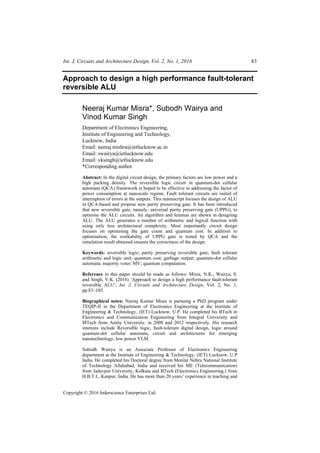
16. 98 N.K. Misra et al.
Proof: A n-bit ALU constructed with four group cells (n × group-1 PP, 1 × group-2 PP
(cell)–1 n × group-2 PP and n × group-3 PP). The quantum cost of F2G, FRG, NFT, and
UPPG are 2, 5, 5 and 8 respectively. The group-1 cell produces 40 quantum cost, group-2
(cell)–1 produces nine quantum cost, group-2 produces 19 quantum cost, group-3
produces seven quantum cost and the F2G produce two quantum cost. Hence, the total
quantum cost can be calculated as follows.
(Group-1 PP Cell) (Group-2 PP Cell) (Group-3 PP Cell)
(Group-2 PP (Cell)–1 F2G
QC(1-bit) QC QC QC
QC QC
= + +
+ +
QC(1-bit) (40 19 7) 9 2 83 66 1 9 2
= + + + + = = × + +
Hence, the statement true for the base case n = 1.
QC(2-bit) 2 40 19 7 9 4 145 (66 2) 9 4
= ×( + + ) + + = = × + +
QC(3-bit) 3 (40 19 7) 9 6 213 (66 3) 9 6
= × + + + + = = × + +
Assume that, the statement true for n = m. Hence, an m-bit fault- tolerant ALU uses
(66m + 9 + 2m) = 68m + 9 quantum cost.
Figure 12 (a) UPPG gate block diagram with four clock zone (b) QCA cell layout of UPPG gate
(c) simulation result of UPPG gate (see online version for colours)
(a)
17. Approach to design a high performance fault-tolerant reversible ALU 99
Figure 12 (a) UPPG gate block diagram with four clock zone (b) QCA cell layout of UPPG gate
(c) simulation result of UPPG gate (continued) (see online version for colours)
(b)
(c)
18. 100 N.K. Misra et al.
6 QCA implementation of UPPG gate
To delineate the use of new types of proposed UPPG gate in nanotechnology, we select
QCA. Since QCA rooted design has high computing speed, high packing density and no
loss of power in signal transition and propagation. It is extravagant that fan-out is not
accredited in reversible logic, but it has been acknowledged in molecular QCA (Thapliyal
and Ranganathan, 2009). The QCA layout of UPPG gate is depicted in Figure 12(b). This
QCA layout design with a 11 majority voter gate, six inverters, 233 cell complexity,
covers an area of 0.29 µm2
and clock cycle delay (latency) of 2.50. The QCA block
diagram of UPPG gate with four clock zone is depicted in Figure 12(a), which four clock
zone is represented by the number next to D (D0 = clock 0, D1 = clock 1, D2 = clock 2
and D3 = clock 4) and MV stand in the majority voter gate. The simulation to test the
workability of UPPG gate with QCA designer and follow the truth table of that gate
(Table 1). For the simulation result of UPPG gate is depicted in Figure 12(c). It has four
output waveform for P, Q, R and S. The first output signal P is obtained after 0.50 clock
cycle delay (latency), Q and R output after one clock cycle delay and the S output is zero
clock cycle delay. From Figure 12(c), we can see that polarisation value of all the four
output signals is fairly better.
7 The performance Tables 4, 5 and 6 of proposed design
It is explicitly from Table 5 that the proposed ALU design is more cost effective
compared to that of existing ALU design. Operational capacity of the proposed UPPG
gate is investigated by synthesising the most used functions such as AND, OR, XOR,
XNOR, NAND, NOR, inverter and signal duplication. A comparative performance result
of the proposed UPPG gate and the available reversible gate is stated in Table 4.The
Table 4 outcomes show that the proposed UPPG is more competent that the available
reversible gates in terms of operational capacity. Table 6 outlines the UPPG gate in QCA
cell layout in terms of complexity, latency, total area and cell area. We have used normal
cells with no any crossovers to enhance the QCA layout stability and efficiency. The
efficiency of UPPG gate layout structure can be confirmed by the cell complexity, total
area and latency. The proposed UPPG gate layout in QCA expressed by majority and
minority voter gate by equations (6), (7) and (8).
( )
P M(M(A, B, D), M(A, B, D), B A B D,
= = ⊕ ⊕ (6)
( ) ( )
( )
Q M M M(C, D, 0), A, 0 , M M(C, D, 0), A, 0 ,1 A CD,
= = ⊕ (7)
( ) ( )
( )
R M M M(C, D,1), A, 0 , M M(C, D,1), A, 0 ,1 A (C D)
= = ⊕ + (8)
19. Approach to design a high performance fault-tolerant reversible ALU 101
Table 4 Performance comparison result of proposed and existing reversible gate
Operational capacity F2G FRG NFT TG PPHCG MIG UPPG (proposed)
XOR Yes No Yes No Yes Yes Yes
XNOR No No No No Yes No Yes
AND No Yes Yes Yes No Yes Yes
OR No No No Yes No No Yes
INVERTER No No Yes Yes No Yes Yes
Signal duplication Yes Yes No Yes Yes Yes Yes
NAND No No No No No Yes Yes
NOR No No No No No No Yes
TLC 2α 2α + 4β
+ 2δ
3α + 4β
+ 3δ
α + β 8α 3α + 2β
+ 1δ
4α + β
Total clock cycle 1σ 1σ 1σ 1σ 1σ 1σ 1σ
PPG Yes Yes Yes No Yes Yes Y
Table 5 The proposed ALU comparison to other previous circuits
Reversible designs NOG GO CI QC
Number of logical and
arithmetic operations
Fault tolerance
1-bit ALU: proposed 16 25 25 77 32 Yes
Rakshith and Saligram 17 37 33 595 32 Yes
Moallem et al. 6 5 4 25 12 No
Guan et al. 24 12 12 70 32 No
Morrison and Ranganathan 6 2 2 24 6 No
Sen et al. 14 15 10 135 20 No
Table 6 Performance analysis of proposed UPPG gate in QCA
Circuit
Gate count
(majority gate +
inverter)
Cell
coun
t
Latency
(clock
delay)
Total
area
(nm2
)
Cell
area
(nm2
)
Area
usage
(%)
UPPG
gate
11 majority gate +
6 inverters
233 0.50 + 1
+ 1 = 2.50
297,766 75,492 25.35
Notes: α – two input XOR calculation; β – two input and calculation; δ – not calculation;
σ – unit clock cycle; TLC – total logic calculation; PPG – parity preserving gate;
RGate – reversible gate; NOG – number of gates; GO – garbage outputs;
CI – constant input.
8 Conclusions
This paper is mainly focused on the proposed design of high performance fault-tolerant
reversible ALU. We have developed an algorithm to design fault-tolerant ALU. In
addition, we designed a new type of parity preserving gate (UPPG gate), which overcome
the shortcoming of few of 4 × 4 parity preserving gates that cannot synthesise any
Boolean functions but our proposed gate can do this. By using this, the ALU is designed
20. 102 N.K. Misra et al.
with various lemmas and correlated to reversible parameters. Finally, the high
performance, fault tolerant, 1-bit ALU is synthesised total 32 operations by using only
77 quantum cost and 16 gate count. It presents that the proposed ALU has the least gate
count over the existing design and produces only 25 garbage outputs. Moreover, it uses
only 25 constant inputs for implementing 16 logical and 16 arithmetic operations. We
have also presented UPPG gate in QCA framework. The cell layout design reflects that
233 cells, total area of only 29,7766 nm2
and use fewer numbers of the clock zone for
operating. The proposed parity preserving gate and high performance, fault-tolerant ALU
will be useful for implementing the low power digital circuits, nano-circuits in computer,
processor of the computer etc.
References
Bennett, C.H. (1973) ‘Logical reversibility of computation’, IBM Journal of Research and
Development, Vol. 17, No. 6, pp.525–532.
Bernstein, G.H., Hu, W., Hang, Q., Sarveswaran, K. and Lieberman, M. (2004) ‘Electron
beam lithography and liftoff of molecules and DNA rafts’, 4th IEEE Conference on
Nanotechnology, pp.201–203.
Bruce, J.W. et al. (2002) ‘Efficient adder circuits based on a conservative reversible logic gate’,
IEEE Computer Society Annual Symposium on VLSI, pp.74–79.
Chabi, A.M., Sayedsalehi, S., Angizi, S. and Navi, K. (2014) ‘Efficient QCA exclusive-or and
multiplexer circuits based on a nanoelectronic-compatible designing approach’, International
Scholarly Research Notices, Vol. 3, No. 5, pp.200–2008.
Fredkin, E. and Toffoli, T. (2002) Conservative Logic, pp.47–81, Springer, London.
Guan, Z., Li, W., Ding, W., Hang, Y. and Ni, L. (2011) ‘An arithmetic logic unit design based on
reversible logic gates’, IEEE Pacific Rim Conference on Communications, Computers and
Signal Processing, pp.925–931.
Keyes, R. and Landauer, R. (1970) ‘Minimal energy dissipation in logic’, IBM Journal of Research
and Development, Vol. 14, No. 2, pp.153–157.
Landauer, R. (1961) ‘Irreversibility and heat generation in the computing process’, IBM Journal of
Research and Development, Vol. 5, No. 3, pp.183–191.
Lent, C.S., Tougaw, P.D., Porod, W. and Bernstein, G.H. (1993) ‘Quantum cellular automata’,
Nanotechnology, Vol. 4, No. 1, p.49.
Misra, N.K., Wairya, S. and Singh, V.K. (2015) ‘Approaches to design feasible error control
scheme based on reversible series gates’, European Journal of Scientific Research, Vol. 129,
No. 3, pp.224–240.
Moallem, P., Ehsanpour, M., Bolhasani, A. and Montazeri, M. (2014) ‘Optimized reversible
arithmetic logic units’, Journal of Electronics (China), Vol. 31, No. 5, pp.394–405
Morrison, M. and Ranganathan, N. (2011) ‘Design of a reversible ALU based on novel
programmable reversible logic gate structures’, IEEE Computer Society Annual Symposium on
VLSI (ISVLSI), pp.126–131.
Rakshith, T.R. and Saligram, R. (2013) ‘Parity preserving logic based fault tolerant reversible
ALU’, IEEE Conference on Information & Communication Technologies, pp.485–490.
Sen, B., Dutta, M. and Sikdar, B.K. (2014a) ‘Efficient design of parity preserving logic in
quantum-dot cellular automata targeting enhanced scalability in testing’, Microelectronics
Journal, Vol. 45, No. 2, pp.239–248.
Sen, B., Dutta, M., Goswami, M. and Sikdar, B.K. (2014b) ‘Modular design of testable reversible
ALU by QCA multiplexer with increase in programmability’, Microelectronics Journal,
Vol. 45, No. 11, pp.1522–1532.
21. Approach to design a high performance fault-tolerant reversible ALU 103
Sen, B., Dutta, M., Singh, D.K., Saran, D. and Sikdar, B.K. (2012) ‘QCA multiplexer based design
of reversible ALU’, IEEE International Conference on Circuits and Systems (ICCAS),
pp.168–173.
Sen, B., Dutta, M., Some, S. and Sikdar, B.K. (2014c) ‘Realizing reversible computing in QCA
framework resulting in efficient design of testable ALU’, ACM Journal on Emerging
Technologies in Computing Systems (JETC), Vol. 11, No. 3, pp.30–52.
Sen, B., Ganeriwal, S. and Sikdar, B.K. (2013) ‘Reversible logic-based fault-tolerant nanocircuits
in QCA’, ISRN Electronics, pp.1–9.
Snider, G.L., Orlov, A.O., Amlani, I., Bernstein, G.H., Lent, C.S., Merz, J.L. and Porod, W. (1998)
‘Experimental demonstration of quantum-dot cellular automata’, Semiconductor Science and
Technology, Vol. 13, No. 8A, p.A130.
Thapliyal, H. and Ranganathan, N. (2009) ‘Conservative QCA gate (CQCA) for designing
concurrently testable molecular QCA circuit’, IEEE International Conference on VLSI Design,
pp.511–516.
Thomsen, M.K., Glück, R. and Axelsen, H.B. (2010) ‘Reversible arithmetic logic unit for quantum
arithmetic’, Journal of Physics A: Mathematical and Theoretical, Vol. 43, No. 38, pp.382002.
Toffoli, T. (1980) Reversible Computing, Tech. Rep. MIT/LCS/TM-151.
Walus, K., Dysart, T.J., Jullien, G.A. and Budiman, R.A. (2004) ‘QCADesigner: a rapid design and
simulation tool for quantum-dot cellular automata’, IEEE Trans. Nanotech, Vol. 3, No. 1,
pp.26–29.
Zhou, R., Li, Y., Zhang, M. and Hu, B. (2015) ‘Novel design for reversible arithmetic logic unit’,
International Journal of Theoretical Physics, Vol. 54, No. 2, pp.630–644.