Download to read offline
![International Journal of Engineering Research and Development
e-ISSN: 2278-067X, p-ISSN: 2278-800X, www.ijerd.com
Volume 11, Issue 04 (April 2015), PP.72-77
72
High Speed Time Efficient Reversible ALU Based Logic Gate
Structure on Vertex Family
Suman Yadav, Manish Saxena
Bansal Institude of Science and Technology
Abstract:- Programmable reversible logic is emerging as a prospective logic design style for implementation in
modern nanotechnology and quantum computing with minimal impact on circuit heat generation. Recent
advances in reversible logic using and quantum computer algorithms allow for improved computer architecture
and arithmetic logic unit designs. In this paper, the two novel 4*4 reversible logic gates (MRG and PAOG) are
used with minimal delay, and may be configured to produce a variety of logical calculations on fixed output
lines based on programmable select input lines. The proposed ALU design is verified and its advantages over
the only existing ALU design are quantitatively analyzed. The proposed design is synthesized using Xilinx ISE
software and simulated using MODEL SIM 6.5b.
Keywords:- Reversible Gates, Arithmetic Unit (ALU), Garbage Output, Quantum Cost
I. INTRODUCTION
In modern VLSI system power dissipation is very high due to rapid switching of internal signals. The
complexity of VLSI circuits increases with each year due to packing more and more logic elements into smaller
volumes. Hence power dissipation has become the main area of concern in VLSI design. Reversible logic has its
basics from thermodynamics of information processing. According to this, traditional irreversible circuits
generate heat due to the loss of information during computation. In order to avoid this information loss the
conventional circuits are modeled using reversible logic. Landauer [1961] showed that the circuits designed
using irreversible elements dissipate heat due to the loss of information bits [1]. It is proved that the loss of one
bit of information results in dissipation of KT*log2 joules of heat energy where K is the Boltzmann constant and
T is the temperature at which the operation is performed. Benett [1973] showed that this heat dissipation due to
information loss can be avoided if the circuit is designed using reversible logic gates [2]. A gate is considered to
be reversible only if for each and every input there is a unique output assignment. Hence there is a one to one
mapping between the input and output vectors. A reversible logic gate is an n –input, n- output device indicating
that it has same number of inputs and outputs. A circuit that is built from reversible gates is known as reversible
logic circuit. In this paper, we design a 16 bit reversible ALU that can perform eight operations simultaneously.
The eight operations include addition, subtraction, AND, NAND, OR, NOR and XOR. All the modules are
simulated in modalism SE 6.5 and synthesized using Xilinx ISE 14.1.
II. LITRATURE SURVEY
The research on reversible logic is being pursued towards both design and synthesis. In the synthesis of
reversible logic circuits there have been several interesting attempts in the literature such as the work in [2-3]. A
reversible arithmetic logic unit was designed by Thomsen, Gluck, and Axelsen [4] that was based on the V-
shaped design of the Van Rentergem adder [5]. The ALU had five fixed select lines, and produced the following
logical outputs: ADD, SUB, NSUB, XOR and NOP. The least significant bit comprised of two Feynman gates
and two Toffoli gates. Each additional bit also had two Fredkin gates.
Asher Peres:- This article is concerned with the construction of a quantum-mechanical Hamiltonian
describing a computer. This Hamiltonian generates a dynamical evolution which mimics a sequence of
elementary logical steps. This can be achieved if each logical step is locally reversible (global reversibility is
insufficient). Computational errors due to noise can be corrected by means of redundancy. In particular,
reversible error-correcting codes can be embedded in the Hamiltonian itself. An estimate is given for the
minimum amount of entropy which must be dissipated at a given noise level and tolerated error rate.
Raghava Garipelly et al. “A Review on Reversible Logic
Gates and their Implementation”, International Journal of Emerging Technology and Advanced
Engineering in this paper the Reversible logic is one of the most vital issue at present time and it has different
areas for its application, those are low power CMOS, quantum computing, nanotechnology, cryptography,
optical computing, DNA computing, digital signal processing (DSP), quantum dot cellular automata,
communication, computer graphics. It is not possible to realize quantum computing without implementation of](https://image.slidesharecdn.com/h1147277-150529052228-lva1-app6892/85/High-Speed-Time-Efficient-Reversible-ALU-Based-Logic-Gate-Structure-on-Vertex-Family-1-320.jpg)
![International Journal of Engineering Research and Development
e-ISSN: 2278-067X, p-ISSN: 2278-800X, www.ijerd.com
Volume 11, Issue 04 (April 2015), PP.72-77
72
High Speed Time Efficient Reversible ALU Based Logic Gate
Structure on Vertex Family
Suman Yadav, Manish Saxena
Bansal Institude of Science and Technology
Abstract:- Programmable reversible logic is emerging as a prospective logic design style for implementation in
modern nanotechnology and quantum computing with minimal impact on circuit heat generation. Recent
advances in reversible logic using and quantum computer algorithms allow for improved computer architecture
and arithmetic logic unit designs. In this paper, the two novel 4*4 reversible logic gates (MRG and PAOG) are
used with minimal delay, and may be configured to produce a variety of logical calculations on fixed output
lines based on programmable select input lines. The proposed ALU design is verified and its advantages over
the only existing ALU design are quantitatively analyzed. The proposed design is synthesized using Xilinx ISE
software and simulated using MODEL SIM 6.5b.
Keywords:- Reversible Gates, Arithmetic Unit (ALU), Garbage Output, Quantum Cost
I. INTRODUCTION
In modern VLSI system power dissipation is very high due to rapid switching of internal signals. The
complexity of VLSI circuits increases with each year due to packing more and more logic elements into smaller
volumes. Hence power dissipation has become the main area of concern in VLSI design. Reversible logic has its
basics from thermodynamics of information processing. According to this, traditional irreversible circuits
generate heat due to the loss of information during computation. In order to avoid this information loss the
conventional circuits are modeled using reversible logic. Landauer [1961] showed that the circuits designed
using irreversible elements dissipate heat due to the loss of information bits [1]. It is proved that the loss of one
bit of information results in dissipation of KT*log2 joules of heat energy where K is the Boltzmann constant and
T is the temperature at which the operation is performed. Benett [1973] showed that this heat dissipation due to
information loss can be avoided if the circuit is designed using reversible logic gates [2]. A gate is considered to
be reversible only if for each and every input there is a unique output assignment. Hence there is a one to one
mapping between the input and output vectors. A reversible logic gate is an n –input, n- output device indicating
that it has same number of inputs and outputs. A circuit that is built from reversible gates is known as reversible
logic circuit. In this paper, we design a 16 bit reversible ALU that can perform eight operations simultaneously.
The eight operations include addition, subtraction, AND, NAND, OR, NOR and XOR. All the modules are
simulated in modalism SE 6.5 and synthesized using Xilinx ISE 14.1.
II. LITRATURE SURVEY
The research on reversible logic is being pursued towards both design and synthesis. In the synthesis of
reversible logic circuits there have been several interesting attempts in the literature such as the work in [2-3]. A
reversible arithmetic logic unit was designed by Thomsen, Gluck, and Axelsen [4] that was based on the V-
shaped design of the Van Rentergem adder [5]. The ALU had five fixed select lines, and produced the following
logical outputs: ADD, SUB, NSUB, XOR and NOP. The least significant bit comprised of two Feynman gates
and two Toffoli gates. Each additional bit also had two Fredkin gates.
Asher Peres:- This article is concerned with the construction of a quantum-mechanical Hamiltonian
describing a computer. This Hamiltonian generates a dynamical evolution which mimics a sequence of
elementary logical steps. This can be achieved if each logical step is locally reversible (global reversibility is
insufficient). Computational errors due to noise can be corrected by means of redundancy. In particular,
reversible error-correcting codes can be embedded in the Hamiltonian itself. An estimate is given for the
minimum amount of entropy which must be dissipated at a given noise level and tolerated error rate.
Raghava Garipelly et al. “A Review on Reversible Logic
Gates and their Implementation”, International Journal of Emerging Technology and Advanced
Engineering in this paper the Reversible logic is one of the most vital issue at present time and it has different
areas for its application, those are low power CMOS, quantum computing, nanotechnology, cryptography,
optical computing, DNA computing, digital signal processing (DSP), quantum dot cellular automata,
communication, computer graphics. It is not possible to realize quantum computing without implementation of](https://image.slidesharecdn.com/h1147277-150529052228-lva1-app6892/75/High-Speed-Time-Efficient-Reversible-ALU-Based-Logic-Gate-Structure-on-Vertex-Family-1-2048.jpg)
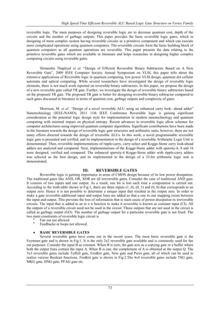
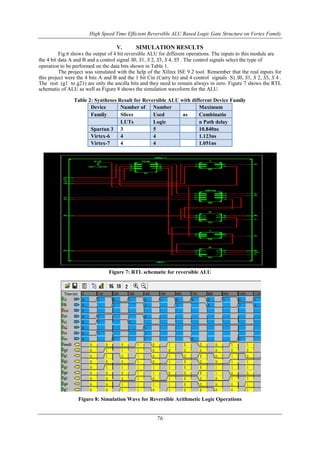
![High Speed Time Efficient Reversible ALU Based Logic Gate Structure on Vertex Family
74
Figure 2: Fredkin gate
Fig.3 shows the TSG gate. Some of the 4x4 gates are designed for implementing some important
combinational functions in addition to the basic functions. Most of the above mentioned gates can be used in the
design of reversible adders.
Figure 3: Peres gate
Several 4x4 and 5x5 gates have been described in the literature targeting low cost and delay which may
be implemented in a programmable manner to produce a high number of logical calculations. The HNG gate,
presented in [10], produces the following logical output calculations:
P A (1) and the logical results based on the input opcodes are presented in Table 1.
(4)
The quantum cost and delay of the HNG is 6. When D = 0,the logical calculations produced on the R and S
outputs are the required sum and carry-out operations for a full adder. The quantum representation of the
HNG is presented in Fig. 4.](https://image.slidesharecdn.com/h1147277-150529052228-lva1-app6892/85/High-Speed-Time-Efficient-Reversible-ALU-Based-Logic-Gate-Structure-on-Vertex-Family-3-320.jpg)
![High Speed Time Efficient Reversible ALU Based Logic Gate Structure on Vertex Family
77
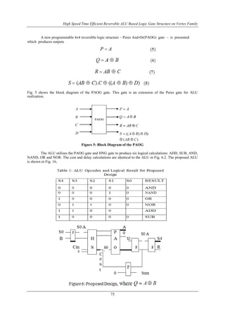
VI. CONCLUSION
The 4bit reversible ALU is designed by integrating various sub modules that includes adder/subtract or,
and logical unit. The logical unit performs AND, OR, NOR, XOR, NAND. The performance evaluation of the
various sub modules are carried out using Modalism 6.5 tools and it was found that the circuits designed using
reversible logic showed a reduced delay and power. As a future work more arithmetic and logical function can
be used.
REFERENCES
[1]. H. Thapliyal and N. Ranganathan, "Design of Efficient Reversible Binary Subtractors Based oNew
Reversible Gate," Proc. of the I Computer Society Annual Symposium on VLSI, 2009.
[2]. M. Morrison and N. Ranganathan, "Design of a Reversible ALU Based on Novel Programmable
Reversible Logic Gate Structures," IEEE International Symposium on VLSI, 2011, pp. 126-131.
[3]. M. Haghparast, S. J. Jassbi, K. Navi and O. Hashemipour, “Design of a NovelReversible
Multiplier Circuit using HNG Gate in Nanotechnology”, World Applied Sci. J., Vol. 3, , 2008, pp.
974-978.
[4]. H. Thapliyal, N. Ranganathan, and R. Ferreira, "Design of a Comparator Tree Based on Reversible
Logic," 10th Proceedings of the IEEE International Conference on Nanotechnology, 2010, pp 1113-
6.
[5]. P. Gupta, A. Agarwal, and N. K. Jha. An algorithm for synthesis of reversible logic ciruits. IEEE
Trans. Computer-Aided Design, 25(11):2317–2330, Nov 2006.
[6]. D. Maslov and G. W. Dueck. Reversible cascades with minimal garbage. IEEE Trans. Computer-
Aided Design, 23(11):1497–1509, November 2004.
[7]. M. Nachtigal and N. Ranganathan. Design and analysis of a novel reversible en-coder/decoder. In
Nanotechnology (IEEE-NANO), 2011 11th IEEE Conference on,pages 1543 –1546, aug. 2011.
[8]. James Donald and Niraj K. Jha. Reversible logic synthesis with fredkin and peres gates. J. Emerg.
Technol. Comput. Syst., 4:2:1–2:19, April 2008.
[9]. Oleg Golubitsky and Dmitri Maslov. A study of optimal 4-bit reversible toffoli circuits and their
synthesis. IEEE Transactions on Computers, 99(PrePrints), 2011.
[10]. Oleg Golubitsky, Sean M. Falconer, and Dmitri Maslov. Synthesis of the optimal 4-bit reversible
circuits. In Proceedings of the 47th Design Automation Conference, DAC ’10, pages 653–656, New
York, NY, USA, 2010. ACM.](https://image.slidesharecdn.com/h1147277-150529052228-lva1-app6892/85/High-Speed-Time-Efficient-Reversible-ALU-Based-Logic-Gate-Structure-on-Vertex-Family-6-320.jpg)

This document summarizes a research paper on designing a high-speed, time-efficient reversible arithmetic logic unit (ALU) using novel reversible logic gates. The paper proposes two new 4x4 reversible logic gates, the MRG and PAOG gates, that can be configured to perform various logical calculations with minimal delay. An 16-bit reversible ALU design is presented that can perform eight operations simultaneously using these gates. The ALU design is verified through simulation in ModelSim 6.5 and synthesis using Xilinx ISE 14.1 software. Analysis shows the proposed ALU design has advantages over existing designs in terms of speed, efficiency and logical functionality.