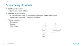
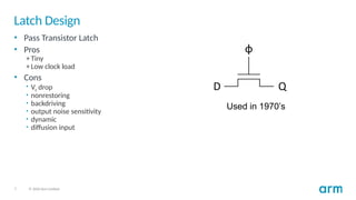
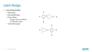
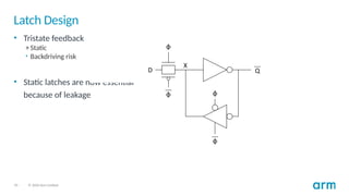
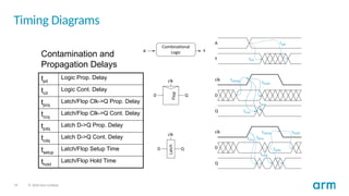
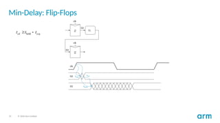
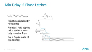
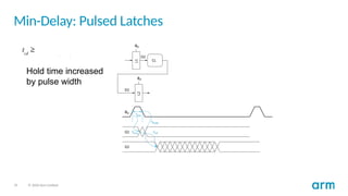
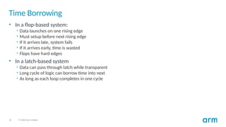
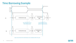
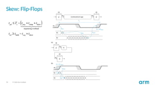
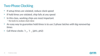
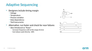
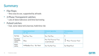
CMOS VLSI Design
Lecture 12:
Sequential
Circuit Design
2 © 2020 Arm Limited
Learning Objectives
At the end of this lecture, you should be able to:
• Describe input data timing constraint limits in relation to setup and hold time
requirements in sequential circuits.
• Describe output data timing constraint limits in relation to propagation delay and
contamination delay requirements in sequential circuits.
• Describe the impact of skew on timing
• Explain time borrowing and describe how it can be applied using latches.
3 © 2020 Arm Limited
Sequencing
• Combinational logic
• output depends on current inputs
• Sequential logic
• output depends on current and previous inputs
• requires separating previous, current, future
• called state or tokens
• E.g., FSM, pipeline
CL
clk
in out
clk clk clk
CL CL
Pipeline
Finite State Machine
4 © 2020 Arm Limited
Sequencing Cont.
• If tokens moved through pipeline at a constant speed, no sequencing elements would
be necessary
• E.g., fiber-optic cable
• Light pulses (tokens) are sent down the cable
• Next pulse is sent before the first reaches the end of cable
• No need for hardware to separate pulses
• But dispersion sets min time between pulses
• This is called wave pipelining in circuits
• In most circuits, dispersion is high
• Delay fast tokens so they don’t catch slow ones.
5 © 2020 Arm Limited
Sequencing Overhead
• Use flip-flops to delay fast tokens so they move through exactly one stage each cycle.
• Inevitably adds some delay to the slow tokens
• Makes circuit slower than just the logic delay
• Called sequencing overhead
• Some people call this clocking overhead
• But it applies to asynchronous circuits too
• Inevitable side effect of maintaining sequence
6 © 2020 Arm Limited
Sequencing Elements
• Latch: Level sensitive
• transparent latch, D latch
• Flip-flop: edge-triggered
• JK Flip-flop (two gated SR flip-flops connected in series, clock to the
second SR is inverted), D flip-flop, D register
• Timing Diagrams
• Transparent
• Opaque
• Edge-trigger D
Flop
Latch
Q
clk clk
D Q
clk
D
Q (latch)
Q (flop)
D
Flop
Latch
Q
clk clk
D Q
clk
D
Q (latch)
Q (flop)
7 © 2020 Arm Limited
Latch Design
• Pass Transistor Latch
• Pros
+ Tiny
+ Low clock load
• Cons
• Vt drop
• nonrestoring
• backdriving
• output noise sensitivity
• dynamic
• diffusion input
Used in 1970’s
8 © 2020 Arm Limited
Latch Design
• Transmission gate
+ No Vt drop
- Requires inverted clock
9 © 2020 Arm Limited
Latch Design
• Inverting buffer
+ Restoring
+ No backdriving
+ Fixes either
– Output noise sensitivity
– Or diffusion input
• Inverted output
10 © 2020 Arm Limited
Latch Design
• Tristate feedback
+ Static
• Backdriving risk
• Static latches are now essential
because of leakage
11 © 2020 Arm Limited
Latch Design
• Buffered input
+ Fixes diffusion input
+ Noninverting
12 © 2020 Arm Limited
Latch Design
• Buffered output
+ No backdriving
• Widely used in standard cells
+ Very robust (most important)
- Rather large
- Rather slow (1.5 – 2 FO4 delays)
- High clock loading
13 © 2020 Arm Limited
Latch Design
• Datapath latch
+ smaller
+ faster
- unbuffered input
14 © 2020 Arm Limited
Flip-Flop Design
• Flip-flop is built as a pair of back-to-back latches
15 © 2020 Arm Limited
Enable
• Enable: ignore clock when en = 0
• Mux: increase latch D-Q delay
• Clock Gating: increase en setup time, skew
16 © 2020 Arm Limited
Reset
• Force output low when reset asserted
• Synchronous vs. asynchronous
17 © 2020 Arm Limited
Set/Reset
• Set forces output high when enabled
• Flip-flop with asynchronous set and reset
18 © 2020 Arm Limited
Sequencing Methods
• Flip-flops
• 2-Phase Latches
• Pulsed Latches
19 © 2020 Arm Limited
Timing Diagrams
tpd
Logic Prop. Delay
tcd
Logic Cont. Delay
tpcq
Latch/Flop Clk->Q Prop. Delay
tccq
Latch/Flop Clk->Q Cont. Delay
tpdq
Latch D->Q Prop. Delay
tcdq
Latch D->Q Cont. Delay
tsetup
Latch/Flop Setup Time
thold
Latch/Flop Hold Time
Contamination and
Propagation Delays
20 © 2020 Arm Limited
Max Delay: Flip-Flops
21 © 2020 Arm Limited
Max Delay: 2-Phase Latches
22 © 2020 Arm Limited
Max Delay: Pulsed Latches
23 © 2020 Arm Limited
Min-Delay: Flip-Flops
hold
cd ccq
t t t
 
24 © 2020 Arm Limited
Min-Delay: 2-Phase Latches
Hold time reduced by
nonoverlap
Paradox: hold applies
twice each cycle vs.
only once for flops.
But a flop is made of
two latches!
25 © 2020 Arm Limited
Min-Delay: Pulsed Latches
Hold time increased
by pulse width
26 © 2020 Arm Limited
Time Borrowing
• In a flop-based system:
• Data launches on one rising edge
• Must setup before next rising edge
• If it arrives late, system fails
• If it arrives early, time is wasted
• Flops have hard edges
• In a latch-based system
• Data can pass through latch while transparent
• Long cycle of logic can borrow time into next
• As long as each loop completes in one cycle
27 © 2020 Arm Limited
Time Borrowing Example
28 © 2020 Arm Limited
How Much Borrowing?
 
borrow setup nonoverlap
2
c
T
t t t
  
2-Phase Latches
borrow setup
pw
t t t
 
Pulsed Latches
29 © 2020 Arm Limited
Clock Skew
• We have assumed zero clock skew
• Clocks really have uncertainty in arrival time
• Decreases maximum propagation delay
• Increases minimum contamination delay
• Decreases time borrowing
30 © 2020 Arm Limited
Skew: Flip-Flops
31 © 2020 Arm Limited
Skew: Latches
2-Phase Latches
Pulsed Latches
32 © 2020 Arm Limited
Two-Phase Clocking
• If setup times are violated, reduce clock speed
• If hold times are violated, chip fails at any speed
• In this class, working chips are most important
• No tools to analyze clock skew
• An easy way to guarantee hold times is to use 2-phase latches with big nonoverlap
times
• Call these clocks 1,  2 (ph1, ph2)
33 © 2020 Arm Limited
Safe Flip-Flop
• Past years used flip-flop with nonoverlapping clocks
• Slow – nonoverlap adds to setup time
• But no hold times
• In industry, use a better timing analyzer
• Add buffers to slow signals if hold time is at risk
34 © 2020 Arm Limited
Adaptive Sequencing
• Designers include timing margin
• Voltage
• Temperature
• Process variation
• Data dependency
• Tool inaccuracies
• Alternative: run faster and check for near failures
• Idea introduced as “Razor”
– Increase frequency until at the verge of error
– Can reduce cycle time by ~30%
35 © 2020 Arm Limited
Timing Analysis
• Design tools perform timing analysis given frequency targets
• Generate a report of setup and hold time failures
• Logic synthesis includes timing analysis
• Selection and placement of gates is done to minimize area while satisfying timing
constraints
36 © 2020 Arm Limited
Timing Closure
• Timing closure is the process of modifying a design to satisfy timing
constraints.
• Manual or automated
• Optimizations include
• Circuit topology (e.g., tree adders vs. ripple carry adders)
• Gate selection (e.g., many stages of simple gates vs. fewer stages of complex
gates)
• Gate placement (e.g., keep gates on the critical path near each other)
• Gate sizing (e.g., larger gates on the critical path)
• Leakage family selection (e.g., low-Vt cells on the critical path)
• Buffer insertion
• Wire optimization
• Clock skew optimization
• Also includes adding delay to fix hold time problems
37 © 2020 Arm Limited
Summary
• Flip-Flops:
• Very easy to use, supported by all tools
• 2-Phase Transparent Latches:
• Lots of skew tolerance and time borrowing
• Pulsed Latches:
• Fast, some skew tol & borrow, hold time risk

CMOS VLSI CKSequentialCircuitDesign.pptx

  • 1.
    CMOS VLSI Design Lecture12: Sequential Circuit Design
  • 2.
    2 © 2020Arm Limited Learning Objectives At the end of this lecture, you should be able to: • Describe input data timing constraint limits in relation to setup and hold time requirements in sequential circuits. • Describe output data timing constraint limits in relation to propagation delay and contamination delay requirements in sequential circuits. • Describe the impact of skew on timing • Explain time borrowing and describe how it can be applied using latches.
  • 3.
    3 © 2020Arm Limited Sequencing • Combinational logic • output depends on current inputs • Sequential logic • output depends on current and previous inputs • requires separating previous, current, future • called state or tokens • E.g., FSM, pipeline CL clk in out clk clk clk CL CL Pipeline Finite State Machine
  • 4.
    4 © 2020Arm Limited Sequencing Cont. • If tokens moved through pipeline at a constant speed, no sequencing elements would be necessary • E.g., fiber-optic cable • Light pulses (tokens) are sent down the cable • Next pulse is sent before the first reaches the end of cable • No need for hardware to separate pulses • But dispersion sets min time between pulses • This is called wave pipelining in circuits • In most circuits, dispersion is high • Delay fast tokens so they don’t catch slow ones.
  • 5.
    5 © 2020Arm Limited Sequencing Overhead • Use flip-flops to delay fast tokens so they move through exactly one stage each cycle. • Inevitably adds some delay to the slow tokens • Makes circuit slower than just the logic delay • Called sequencing overhead • Some people call this clocking overhead • But it applies to asynchronous circuits too • Inevitable side effect of maintaining sequence
  • 6.
    6 © 2020Arm Limited Sequencing Elements • Latch: Level sensitive • transparent latch, D latch • Flip-flop: edge-triggered • JK Flip-flop (two gated SR flip-flops connected in series, clock to the second SR is inverted), D flip-flop, D register • Timing Diagrams • Transparent • Opaque • Edge-trigger D Flop Latch Q clk clk D Q clk D Q (latch) Q (flop) D Flop Latch Q clk clk D Q clk D Q (latch) Q (flop)
  • 7.
    7 © 2020Arm Limited Latch Design • Pass Transistor Latch • Pros + Tiny + Low clock load • Cons • Vt drop • nonrestoring • backdriving • output noise sensitivity • dynamic • diffusion input Used in 1970’s
  • 8.
    8 © 2020Arm Limited Latch Design • Transmission gate + No Vt drop - Requires inverted clock
  • 9.
    9 © 2020Arm Limited Latch Design • Inverting buffer + Restoring + No backdriving + Fixes either – Output noise sensitivity – Or diffusion input • Inverted output
  • 10.
    10 © 2020Arm Limited Latch Design • Tristate feedback + Static • Backdriving risk • Static latches are now essential because of leakage
  • 11.
    11 © 2020Arm Limited Latch Design • Buffered input + Fixes diffusion input + Noninverting
  • 12.
    12 © 2020Arm Limited Latch Design • Buffered output + No backdriving • Widely used in standard cells + Very robust (most important) - Rather large - Rather slow (1.5 – 2 FO4 delays) - High clock loading
  • 13.
    13 © 2020Arm Limited Latch Design • Datapath latch + smaller + faster - unbuffered input
  • 14.
    14 © 2020Arm Limited Flip-Flop Design • Flip-flop is built as a pair of back-to-back latches
  • 15.
    15 © 2020Arm Limited Enable • Enable: ignore clock when en = 0 • Mux: increase latch D-Q delay • Clock Gating: increase en setup time, skew
  • 16.
    16 © 2020Arm Limited Reset • Force output low when reset asserted • Synchronous vs. asynchronous
  • 17.
    17 © 2020Arm Limited Set/Reset • Set forces output high when enabled • Flip-flop with asynchronous set and reset
  • 18.
    18 © 2020Arm Limited Sequencing Methods • Flip-flops • 2-Phase Latches • Pulsed Latches
  • 19.
    19 © 2020Arm Limited Timing Diagrams tpd Logic Prop. Delay tcd Logic Cont. Delay tpcq Latch/Flop Clk->Q Prop. Delay tccq Latch/Flop Clk->Q Cont. Delay tpdq Latch D->Q Prop. Delay tcdq Latch D->Q Cont. Delay tsetup Latch/Flop Setup Time thold Latch/Flop Hold Time Contamination and Propagation Delays
  • 20.
    20 © 2020Arm Limited Max Delay: Flip-Flops
  • 21.
    21 © 2020Arm Limited Max Delay: 2-Phase Latches
  • 22.
    22 © 2020Arm Limited Max Delay: Pulsed Latches
  • 23.
    23 © 2020Arm Limited Min-Delay: Flip-Flops hold cd ccq t t t  
  • 24.
    24 © 2020Arm Limited Min-Delay: 2-Phase Latches Hold time reduced by nonoverlap Paradox: hold applies twice each cycle vs. only once for flops. But a flop is made of two latches!
  • 25.
    25 © 2020Arm Limited Min-Delay: Pulsed Latches Hold time increased by pulse width
  • 26.
    26 © 2020Arm Limited Time Borrowing • In a flop-based system: • Data launches on one rising edge • Must setup before next rising edge • If it arrives late, system fails • If it arrives early, time is wasted • Flops have hard edges • In a latch-based system • Data can pass through latch while transparent • Long cycle of logic can borrow time into next • As long as each loop completes in one cycle
  • 27.
    27 © 2020Arm Limited Time Borrowing Example
  • 28.
    28 © 2020Arm Limited How Much Borrowing?   borrow setup nonoverlap 2 c T t t t    2-Phase Latches borrow setup pw t t t   Pulsed Latches
  • 29.
    29 © 2020Arm Limited Clock Skew • We have assumed zero clock skew • Clocks really have uncertainty in arrival time • Decreases maximum propagation delay • Increases minimum contamination delay • Decreases time borrowing
  • 30.
    30 © 2020Arm Limited Skew: Flip-Flops
  • 31.
    31 © 2020Arm Limited Skew: Latches 2-Phase Latches Pulsed Latches
  • 32.
    32 © 2020Arm Limited Two-Phase Clocking • If setup times are violated, reduce clock speed • If hold times are violated, chip fails at any speed • In this class, working chips are most important • No tools to analyze clock skew • An easy way to guarantee hold times is to use 2-phase latches with big nonoverlap times • Call these clocks 1,  2 (ph1, ph2)
  • 33.
    33 © 2020Arm Limited Safe Flip-Flop • Past years used flip-flop with nonoverlapping clocks • Slow – nonoverlap adds to setup time • But no hold times • In industry, use a better timing analyzer • Add buffers to slow signals if hold time is at risk
  • 34.
    34 © 2020Arm Limited Adaptive Sequencing • Designers include timing margin • Voltage • Temperature • Process variation • Data dependency • Tool inaccuracies • Alternative: run faster and check for near failures • Idea introduced as “Razor” – Increase frequency until at the verge of error – Can reduce cycle time by ~30%
  • 35.
    35 © 2020Arm Limited Timing Analysis • Design tools perform timing analysis given frequency targets • Generate a report of setup and hold time failures • Logic synthesis includes timing analysis • Selection and placement of gates is done to minimize area while satisfying timing constraints
  • 36.
    36 © 2020Arm Limited Timing Closure • Timing closure is the process of modifying a design to satisfy timing constraints. • Manual or automated • Optimizations include • Circuit topology (e.g., tree adders vs. ripple carry adders) • Gate selection (e.g., many stages of simple gates vs. fewer stages of complex gates) • Gate placement (e.g., keep gates on the critical path near each other) • Gate sizing (e.g., larger gates on the critical path) • Leakage family selection (e.g., low-Vt cells on the critical path) • Buffer insertion • Wire optimization • Clock skew optimization • Also includes adding delay to fix hold time problems
  • 37.
    37 © 2020Arm Limited Summary • Flip-Flops: • Very easy to use, supported by all tools • 2-Phase Transparent Latches: • Lots of skew tolerance and time borrowing • Pulsed Latches: • Fast, some skew tol & borrow, hold time risk

Editor's Notes

  • #1 Hello and welcome.
  • #3 Combinational logic is implemented using Boolean circuits; they operate without the need of a clock signal and do not contain any form of memory. Thus, their outputs are a function of only their inputs. Sequential logic, on the other hand, is a circuit whose output tracks its present input value and the sequence of its past inputs. Such circuits use state machine or tokens in a pipeline to differentiate the previous, current, and future inputs to the system.
  • #4 Wave pipelining is a circuit design technique to improve the throughput of a logic circuit design without the use of intermediate latches or registers. This allows circuits to be clocked at higher rates. In digital design, extra circuit is used to maintain the sequence of tokens.
  • #5 Flip-flops or latch are used to delay fast tokens. These flip-flops also adds delay to the slow tokens. This makes the sequential circuit slower than just the logic delay. This is known as sequencing overhead.
  • #6 Two elements used in sequencing circuits are Latch and Flip-Flops. Latches are level sensitive, while flip-flops are edge triggered. For latches, the output Q will follow the input D when the clock is active state/high (the latch is open i.e transparent), and the output Q will retain its current value irrespective of a change in input value when the clock is inactive/low. The output of a Flip-Flop, on the other hand, will change state only when the clock signal is changing (low to high or high to low, depending on if it is +ve edge- or –ve edge-triggered, respectively).
  • #7  In this setup, the output Q will follow the input D when the control input on the transistor gate is high. When the control input is low, the output Q will be in impedance state Z. This circuit suffers from voltage variation due to threshold drop (Vt), which is the result of the series resistance between the input and the output.  Nonrestoring here refers to the inability of the circuit to produce a strong output as the input. Depending on the type of pass transistor used, it may result in degraded output leading to reduced noise margins.
  • #8 Pass transistors can be used to form transmission gates. In this setup, the output Q will follow the input D when the control input is high. When the control input is low, the Q will be in impedance state Z. In this setup, the disadvantage of Vt drop in the output in single pass transistor is avoided. However, the second transistor (pmos) requires the inverted input of the control signal.
  • #9 Using a transmission gate with an inverting buffer has its advantages in restoring the output signals (fixing output noise sensitivity if the inverting buffer is at the output) and also stopping backdriving (fixing diffusion input issue). In the first circuit, node X can change state, if for example when the clock is low, Input D is not driving X. Over time the value of X starts degrading across the parasitic capacitance. If the clock is kept low for a long enough time, that X degrades greatly, the output Q_bar may lose its correct value.
  • #10 In this setup, a latch with inverting output is designed by adding a tristate buffer (inverted input) feedback between the output of the inverter and its input. The tristate buffer serves to maintain the input of the inverting buffer when the clock signal goes low and puts the transmission gate’s output in high impedance state. This circuit suffers from backdriving i.e noise at the output can affect the input D.
  • #11 In this setup, a latch is designed by adding an inverting buffer at the input of the transmission gate of the previous latch. This setup also has an advantage in that the input to the circuit is through the gates and not diffusion inputs to the transistors.
  • #12 This circuit is robust, since the output Q is generated using a separate buffer, which eliminates issues with backdriving. The output Q is maintained by the loop which includes the tristate buffer. The extra buffer and its inverted input increases area of the circuit.
  • #13 This datapath latch has the advantage of being smaller and faster, but the input is unbuffered, thus providing diffusion input to the transistors.
  • #14 A flip-flop can be designed using back-to-back latches. In the first circuit, D – X is one latch. Note the change in clock to the inputs of the transmission gates in the both latches.
  • #15 With a multiplexer, the data input to a latch or flip-flop can be controlled with an enable signal. In this setup, the output of the latch/FF is fed into input 0 (input selected when en = 0). This ensures that the output state is maintained, even when input is disabled, and the Latch/FF is triggered by the clock. The use of a multiplexer to gate the input increases the delay from input D to output Q. Enable input can be used to gate the clock; however, this can result in increased clock skew and setup time for the flip-flop/latch.
  • #16 Reset input is used to force the output of the latch low. For asynchronous design, this control is independent of the clock.
  • #17 Just like reset input was added, the circuit can be further modified to include a set input. The set input is used to force the output high. In this circuit, set and reset cannot be asserted at the same time. It will lead to an invalid state.
  • #18 Sequencing can be achieved using: Flip-flops: here the flip-flops are sensitive to the edge of the clock. However, there are factors that must be considered when choosing the minimum clock period to ensure the circuit operates correctly. Two-phase transparent latch can be used in sequencing. Here, the phase difference of both clocks must meet certain conditions for the system to operate correctly. With pulsed latches, since the latch is active at the +ve state of the clock, in this setup, the clock stays briefly at this state and transitions to a low. The pulse should stay long enough for the latch to capture the value of the data at its input.
  • #19 Let’s first define contamination delay and propagation delay. Contamination delay is the minimum time it takes for the output to start changing its value in response to an input signal. At this stage, the output has not fully settled to its correct state. Propagation delay is the minimum time it takes for the output to fully settle at its correct state in response to an input signal. In the table above: tpd and tcd refers to the propagation and contamination delays of the combinational circuit, respectively. tpcq and tccq, respectively, refer to the propagation and contamination delays of the latch/FF output when the clock transitions to a +ve state. tpdq and tcdq, respectively, refer to the propagation and contamination delays of the latch output Q when a change occurs in its input D during the period the clock is high. tsetup for latch/FF refers to the minimum time between when the input signal at D has settled to the time the clock occurs. thold for latch/FF refers to the minimum time that must pass after clock transitions to a low before the input D can change. For the three figures above including their timing diagrams The first figure is a combinational circuit with input A and output Y. The timing diagram shows that the output Y starts responding to a change in A at time tcd. This is called the logic contamination delay. The timing diagram shows that the output Y will settle at the correct state in response to a change in input A at time tpd.This is called the logic propagation delay. During the time between tcd and tpd, the output Y is not stable. The second figure is a Flip-flop with input D and output Q. The timing diagram shows that the data at D must be stable for a minimum time tsetup before the clock transitions high after which the data at D must not change for at least thold time after the clock transitions high. The timing diagram shows that the output Q will start changing after tccq, although not stable until after tpcq. The timings tccq and tpcq are FFs Clock-to-Q contamination and Clock-to-Q propagation delays, respectively. Both timings are relative to the rising edge of the clock. The third figure is a Latch with input D and output Q. The timing diagram shows that when the clock transitions high, the output Q begins to change from tccq to tpcq before Q becomes stable. Both contamination and propagation delays are relative from clock rising to Q. The timing diagram shows that when the clock is high and input D begins to change, Q output gets contaminated at time tcdq, and after D has settled, Q will settle to the new value at tpdq. If D changes when the clock is high, the clock should remain high for at least tsetup time and D must remain stable for at least thold after the clock goes low.
  • #20 Timing diagram illustrates the sequencing overhead associated with this type of circuit. The two factors are tpcq, which is the clock-to-Q1 propagation delay, and tsetup, which is the minimum time output D2 must be stable with the new data before the next positive transition of the clock occurs. The clock period must be larger than or equal to total delay due to the sequencing overhead (tpcq – F1 and tsetup – F2) and the propagation delay tpd of the combinational logic for the circuit to function correctly.
  • #21 Using the timing diagram, when the data D1 arrived at L1, L1 was transparent since clock 1 was high. The sequence of operation is shown thus: Latch 1 - Data propagates from D1 to Q1 after time tpdq1, Combinational Logic 1 - D2 correctly responds to a change in Q1 after time tpd1 Latch 2 - Data propagates from D2 to Q2 after time tpdq2, Combinational Logic 2 – D3 correctly responds to a change in Q2 after timetpd2 If D3 arrives when clock 1 has gone high, but early enough to meet L3 setup time before the clock starts transitioning to a low, then L3 will correctly capture D3. However, with careful design, D3 can arrive within a single clock period of clock 1. That is the period of the first clock cannot be less than the sum of + +.
  • #22 In timing diagram (a), the critical path consists of L1 and combinational logic, and since the pulse width is greater than the setup time, L2 will capture the new data on D2. In timing diagram (b), the pulse width is less than the setup time; therefore, the data at D2 must be present and stable before the pulse rises.
  • #23 Input data at D2 must satisfy hold time of F2. That is, when the clock transition results in a change in Q1, the now soon to be old value of D2 stable, long enough to the hold time requirement of F2 i.e the contamination delay of CL should meet the hold time requirement of F2 Therefore, the minimum logic contamination delay is given by the equation above.
  • #24 Input data at D2 must satisfy hold time of L2. That is, when the clock transition results in a change in Q1, the now soon to be old value of D2 stable, long enough to the hold time requirement of L2 i.e the contamination delay of CL should meet the hold time requirement of L2 Therefore, the minimum logic contamination delay is given by the equation above.
  • #25  Min-delay timing constraints on a path from one pulsed latch to the next. Here, data at D2 must not change until after the falling edge of the pulse plus the hold time of L2.
  • #26 Time borrowing In a Flip-flop based system, the data is captures at the rising edge of the clock. The data must meet setup requirements before the next rising edge of the clock else the system may fail. If the data arrives very early, then time will be wasted. In latch-based design, data can pass through latch while transparent. Using multiple clocks, the designer can ensure that time is not wasted.
  • #27 Timing diagram illustrates time borrowing. In the illustration above, notice that the two clocks are complements of each other. In system (a), latch 1 captures the data at its input when clock 1 is high. If the propagation delay in the first combinational logic is high, such that its output is valid when clock 1 becomes low, then the second latch which is now transparent will correctly capture the new data. If the propagation delay of the second combinational logic is small enough and the setup time requirement of the third latch is met before clock 1 transitions high again the system will operate correctly. Note that the combined propagation delay of the system must be less than the period of clock 1. In system (b) latch 1 will capture the new data at the output of combinational logic 2 so if the total propagation delay of the system is less than the period of clock 1.
  • #28 Figure illustrates a two-phase latch system and the time it can borrow.
  • #29 Uncertainty at clock arrival times for different components must be considered when designing circuits. This certainly affects the calculations of minimum, maximum delays and time borrowing.
  • #30 Clock skew can also affect the contamination delay of FF-based sequential circuits.
  • #31 Clock skew can also affect the contamination delay of 2-phase latch and pulsed latch-based sequential circuits.
  • #34 Timing margins can be affected by voltage, temperature, process variation, data dependency, and tool inaccuracies. These factors are considered by designers, so time margins are included in design specification. Another method is a run a faster clock and then check for near failures. The circuit in this slide will indicate an error in the instance where the clock is high and D input changes to a new value. This is because the latch will update its output, while the FF will still maintain its output until next rising edge of the clock.
  • #35 CAD tools can be used to generate a report of setup and hold time failures. These tools optimize the placement of gates to minimize area while satisfying timing constraints.