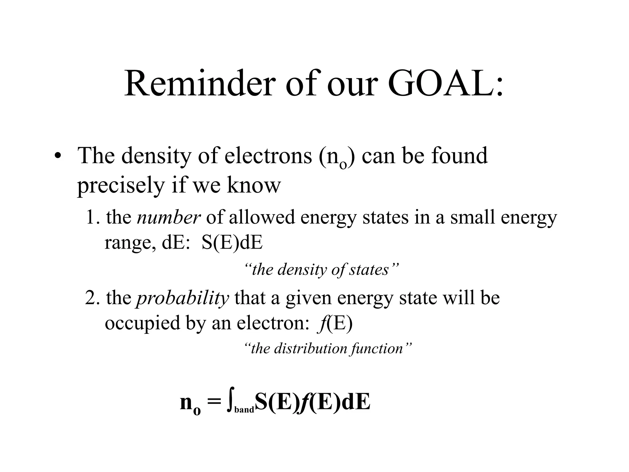
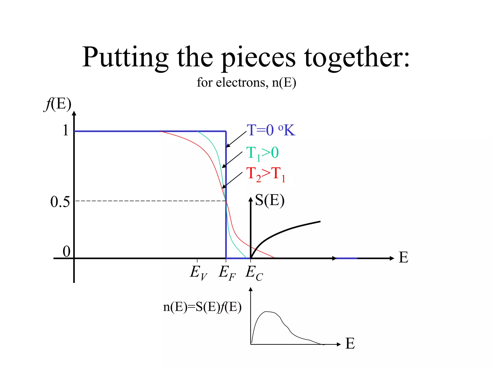
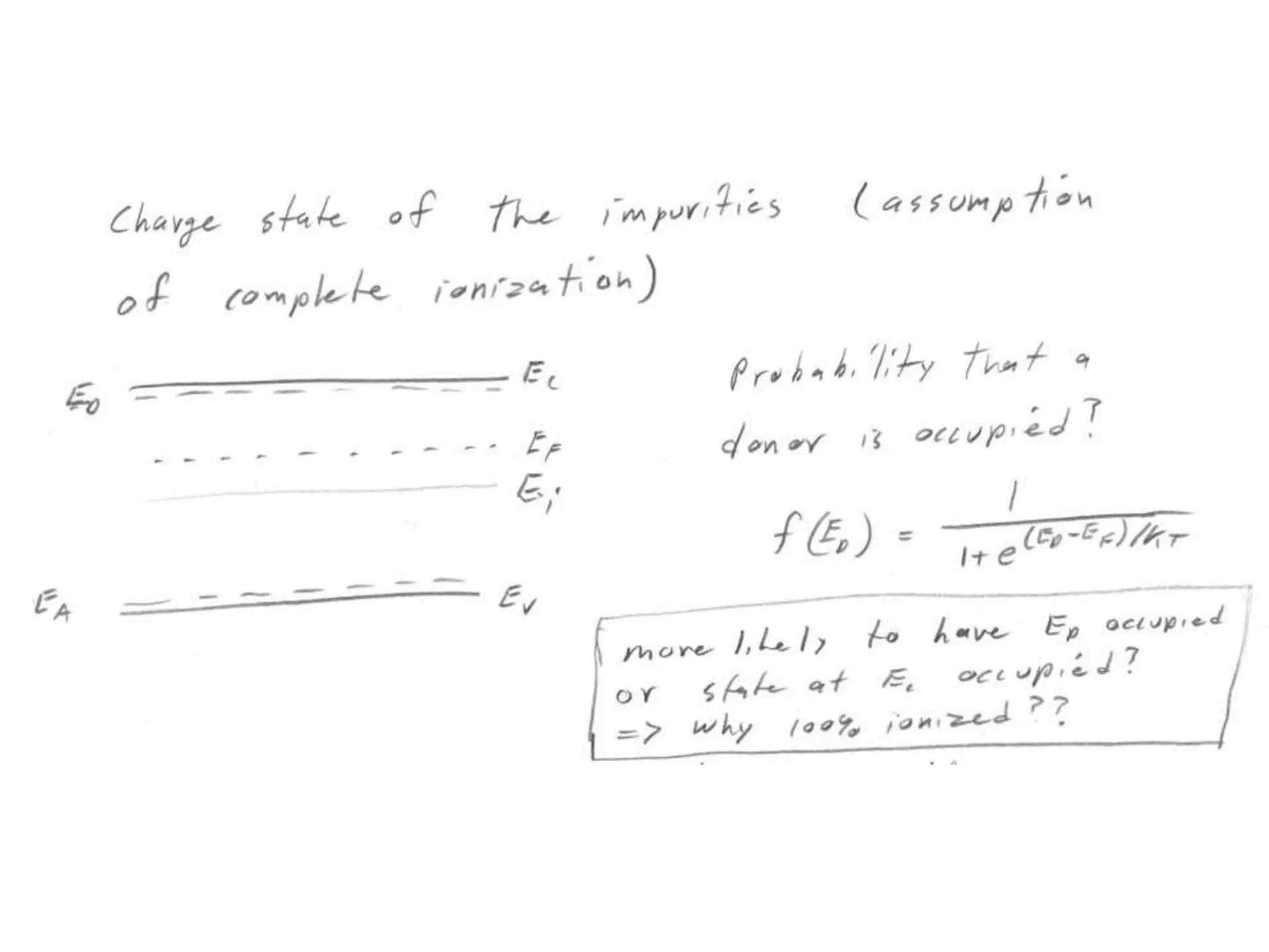
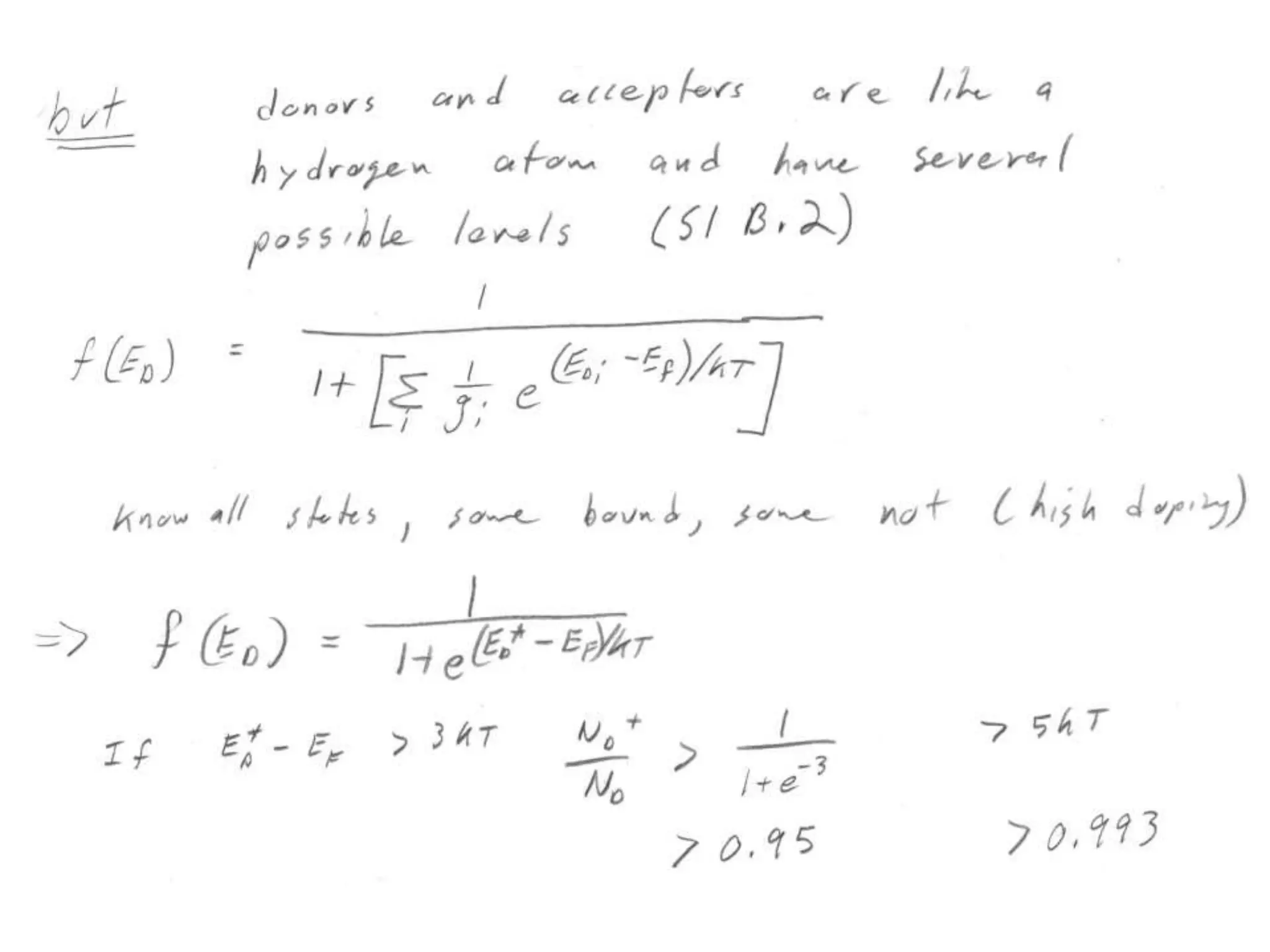
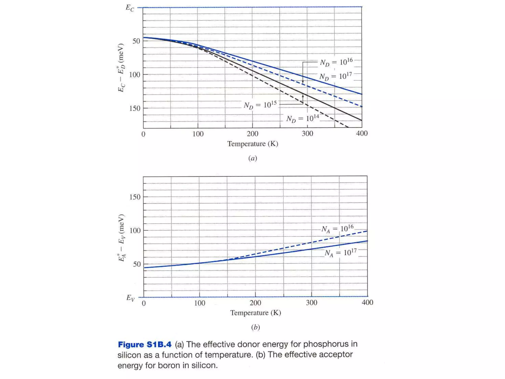
The document discusses carrier concentration calculations in semiconductors. It defines density of states and distribution functions, which are used to calculate the number of electrons and holes. The Fermi-Dirac distribution gives the probability that an energy state is occupied. For non-degenerate semiconductors, the intrinsic carrier concentration is proportional to the exponential of the bandgap divided by temperature. For degenerate semiconductors with high doping, the Fermi level moves into the bands and the effective bandgap is reduced.


![Fermi-Dirac Distribution
The probability that an electron occupies an
energy level, E, is
f(E) = 1/{1+exp[(E-EF)/kT]}
– where T is the temperature (Kelvin)
– k is the Boltzmann constant (k=8.62x10⁻⁵ eV/K)
– EF is the Fermi Energy (in eV)
– (Can derive this – statistical mechanics.)](https://image.slidesharecdn.com/homogeneoussemiconductors0801c-220811095648-27c6414c/75/Homogeneous_Semiconductors0801c-ppt-13-2048.jpg)
![f(E) = 1/{1+exp[(E-EF)/kT]}
All energy levels are filled with e-’s below the Fermi Energy at 0 oK
f(E)
1
0
EF
E
T=0 oK
T1>0
T2>T1
0.5](https://image.slidesharecdn.com/homogeneoussemiconductors0801c-220811095648-27c6414c/75/Homogeneous_Semiconductors0801c-ppt-14-2048.jpg)
![Fermi-Dirac Distribution for holes
Remember, a hole is an energy state that is NOT occupied by
an electron.
Therefore, the probability that a state is occupied by a hole
is the probability that a state is NOT occupied by an electron:
fp(E) = 1 – f(E) = 1 - 1/{1+exp[(E-EF)/kT]}
={1+exp[(E-EF)/kT]}/{1+exp[(E-EF)/kT]} -
1/{1+exp[(E-EF)/kT]}
= {exp[(E-EF)/kT]}/{1+exp[(E-EF)/kT]}
=1/{1+ exp[(EF - E)/kT]}](https://image.slidesharecdn.com/homogeneoussemiconductors0801c-220811095648-27c6414c/75/Homogeneous_Semiconductors0801c-ppt-15-2048.jpg)
![The Boltzmann Approximation
If (E-EF)>kT such that exp[(E-EF)/kT] >> 1 then,
f(E) = {1+exp[(E-EF)/kT]}-1 {exp[(E-EF)/kT]}-1
exp[-(E-EF)/kT] …the Boltzmann approx.
similarly, fp(E) is small when exp[(EF - E)/kT]>>1:
fp(E) = {1+exp[(EF - E)/kT]}-1 {exp[(EF - E)/kT]}-1
exp[-(EF - E)/kT]
If the Boltz. approx. is valid, we say the semiconductor is non-degenerate.](https://image.slidesharecdn.com/homogeneoussemiconductors0801c-220811095648-27c6414c/75/Homogeneous_Semiconductors0801c-ppt-16-2048.jpg)

![Finding no and po
2
/
3
2
*
/
2
/
3
2
*
2
(min)
0
2
2
...
]
/
)
(
exp[
2
2
1
)
(
)
(
kT
m
N
where
kT
E
E
N
dE
e
E
E
m
dE
E
f
E
S
p
dsh
V
V
F
V
kT
E
E
Ev
V
dsh
Ev
Ev
p
F
2
/
3
2
*
/
2
/
3
2
*
2
(max)
0
2
2
...
]
/
)
(
exp[
2
2
1
)
(
)
(
kT
m
N
where
kT
E
E
N
dE
e
E
E
m
dE
E
f
E
S
n
dse
C
F
C
C
kT
E
E
Ec
C
dse
Ec
Ec
F
the effective density of states
at EC
the effective density of states
at EV](https://image.slidesharecdn.com/homogeneoussemiconductors0801c-220811095648-27c6414c/75/Homogeneous_Semiconductors0801c-ppt-19-2048.jpg)

![Energy Band Diagram
n-type semiconductor: no>po
conduction band
valence band
EC
EV
x
E(x)
n(E)
p(E)
EF
]
/
)
(
exp[
0 kT
E
E
N
n F
C
C
nopo=ni
2](https://image.slidesharecdn.com/homogeneoussemiconductors0801c-220811095648-27c6414c/75/Homogeneous_Semiconductors0801c-ppt-21-2048.jpg)
![Energy Band Diagram
p-type semiconductor: po>no
conduction band
valence band
EC
EV
x
E(x)
n(E)
p(E) EF
]
/
)
(
exp[
0 kT
E
E
N
p V
F
V
nopo=ni
2](https://image.slidesharecdn.com/homogeneoussemiconductors0801c-220811095648-27c6414c/75/Homogeneous_Semiconductors0801c-ppt-22-2048.jpg)
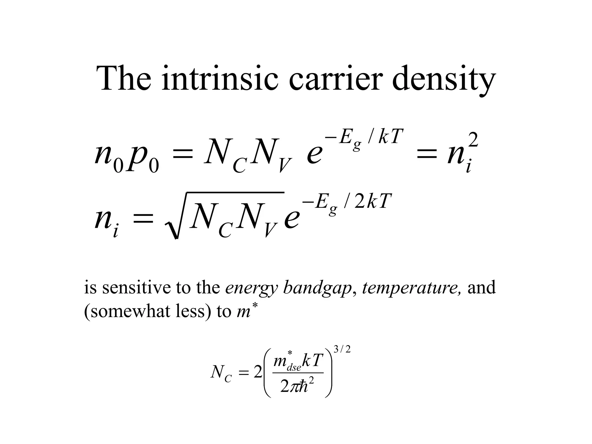
![A very useful relationship
kT
E
V
C
kT
Ev
Ec
V
C
V
F
V
F
C
C
g
e
N
N
e
N
N
kT
E
E
N
kT
E
E
N
p
n
/
/
)
(
0
0 ]
/
)
(
exp[
]
/
)
(
exp[
…which is independent of the Fermi Energy
Recall that ni = no= po for an intrinsic semiconductor, so
nopo = ni
2
for all non-degenerate semiconductors.
(that is as long as EF is not within a few kT of the band edge)
kT
E
V
C
i
i
kT
E
V
C
g
g
e
N
N
n
n
e
N
N
p
n
2
/
2
/
0
0
](https://image.slidesharecdn.com/homogeneoussemiconductors0801c-220811095648-27c6414c/75/Homogeneous_Semiconductors0801c-ppt-23-2048.jpg)
![The intrinsic Fermi Energy (Ei)
]
/
)
(
exp[
]
/
)
(
exp[ kT
E
E
N
kT
E
E
N V
i
V
i
C
C
For an intrinsic semiconductor, no=po and EF=Ei
which gives
Ei = (EC + EV)/2 + (kT/2)ln(NV/NC)
so the intrinsic Fermi level is approximately
in the middle of the bandgap.](https://image.slidesharecdn.com/homogeneoussemiconductors0801c-220811095648-27c6414c/75/Homogeneous_Semiconductors0801c-ppt-25-2048.jpg)


![Higher Temperatures
Consider a semiconductor doped with NA ionized
acceptors (-q) and ND ionized donors (+q), do not assume
that ni is small – high temperature expression.
positive charges = negative charges
po + ND = no + NA
using ni
2 = nopo
ni
2/no + ND = no+ NA
ni
2 + no(ND-NA) - no
2 = 0
no = 0.5(ND-NA) 0.5[(ND-NA)2 + 4ni
2]1/2
we use the ‘+’solution since no should be increased by ni
no = ND - NA in the limit that ni<<ND-NA](https://image.slidesharecdn.com/homogeneoussemiconductors0801c-220811095648-27c6414c/75/Homogeneous_Semiconductors0801c-ppt-38-2048.jpg)


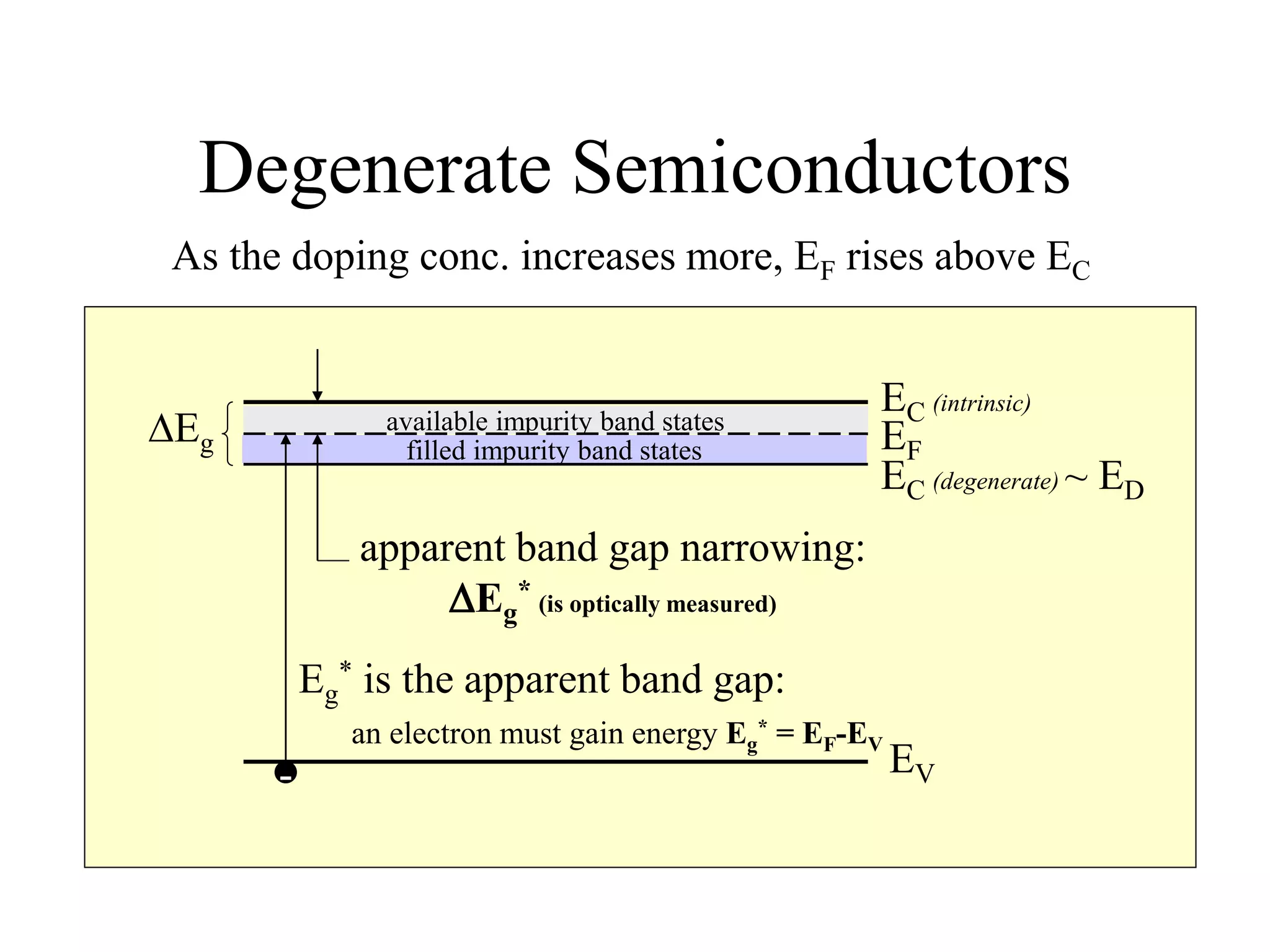
![Electron Concentration
in degenerately doped n-type semiconductors
The donors are fully ionized: no = ND
The holes still follow the Boltz. approx. since EF-EV>>>kT
po = NV exp[-(EF-EV)/kT] = NV exp[-(Eg
*)/kT]
= NV exp[-(Ego- DEg
*)/kT]
= NV exp[-Ego/kT]exp[DEg
*)/kT]
nopo = NDNVexp[-Ego/kT] exp[DEg
*)/kT]
= (ND/NC) NCNVexp[-Ego/kT] exp[DEg
*)/kT]
= (ND/NC)ni
2 exp[DEg
*)/kT]](https://image.slidesharecdn.com/homogeneoussemiconductors0801c-220811095648-27c6414c/75/Homogeneous_Semiconductors0801c-ppt-47-2048.jpg)
![Summary
non-degenerate:
nopo= ni
2
degenerate n-type:
nopo= ni
2 (ND/NC) exp[DEg
*)/kT]
degenerate p-type:
nopo= ni
2 (NA/NV) exp[DEg
*)/kT]](https://image.slidesharecdn.com/homogeneoussemiconductors0801c-220811095648-27c6414c/75/Homogeneous_Semiconductors0801c-ppt-48-2048.jpg)


