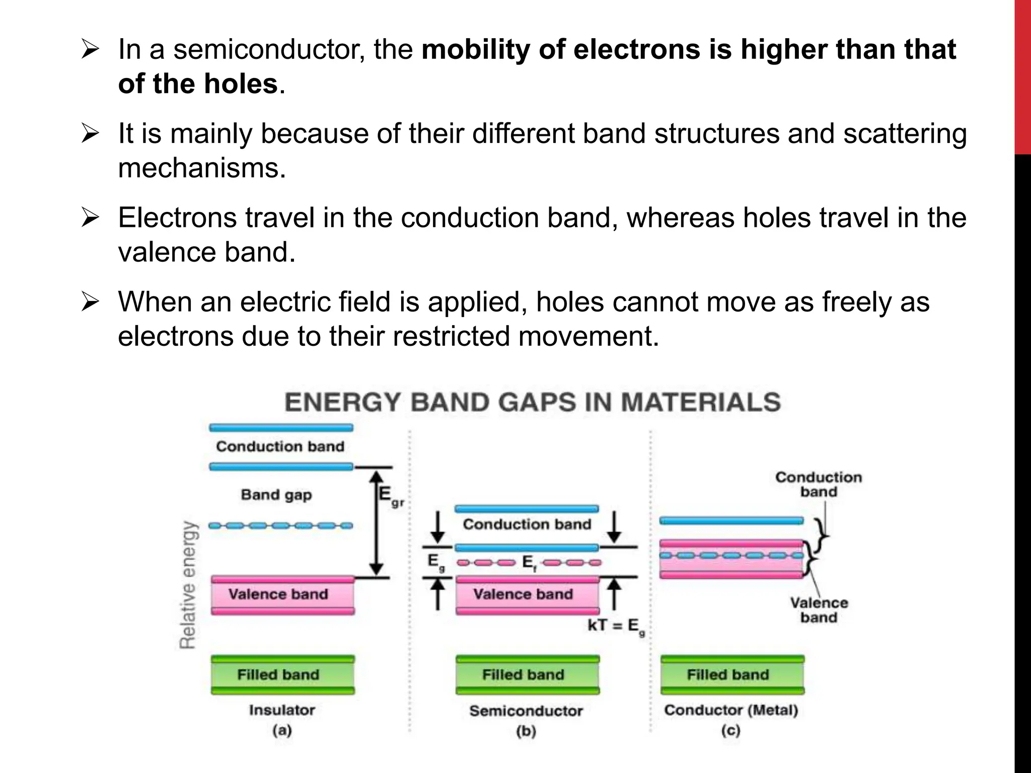
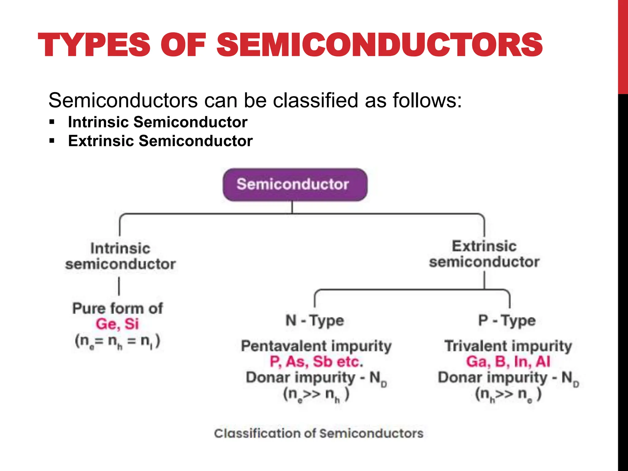
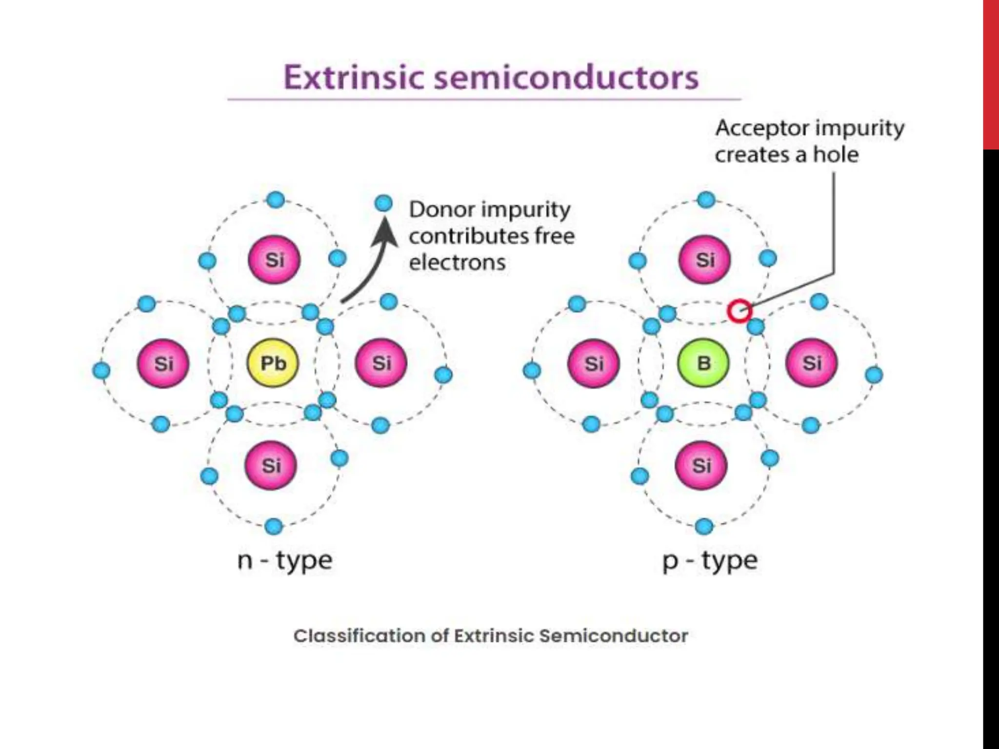
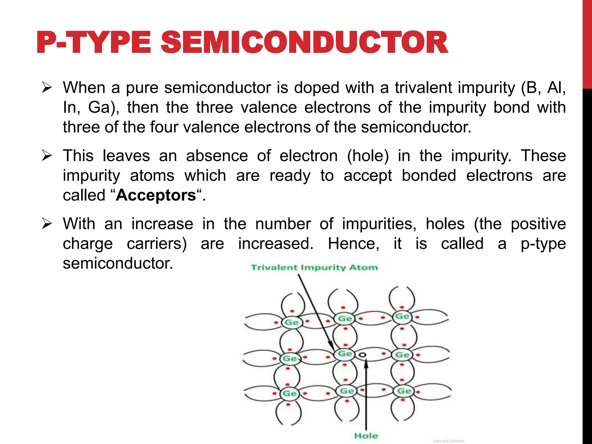
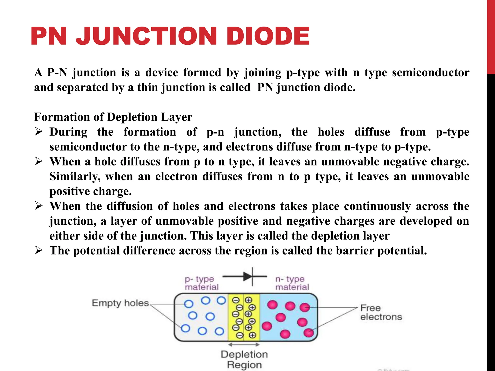
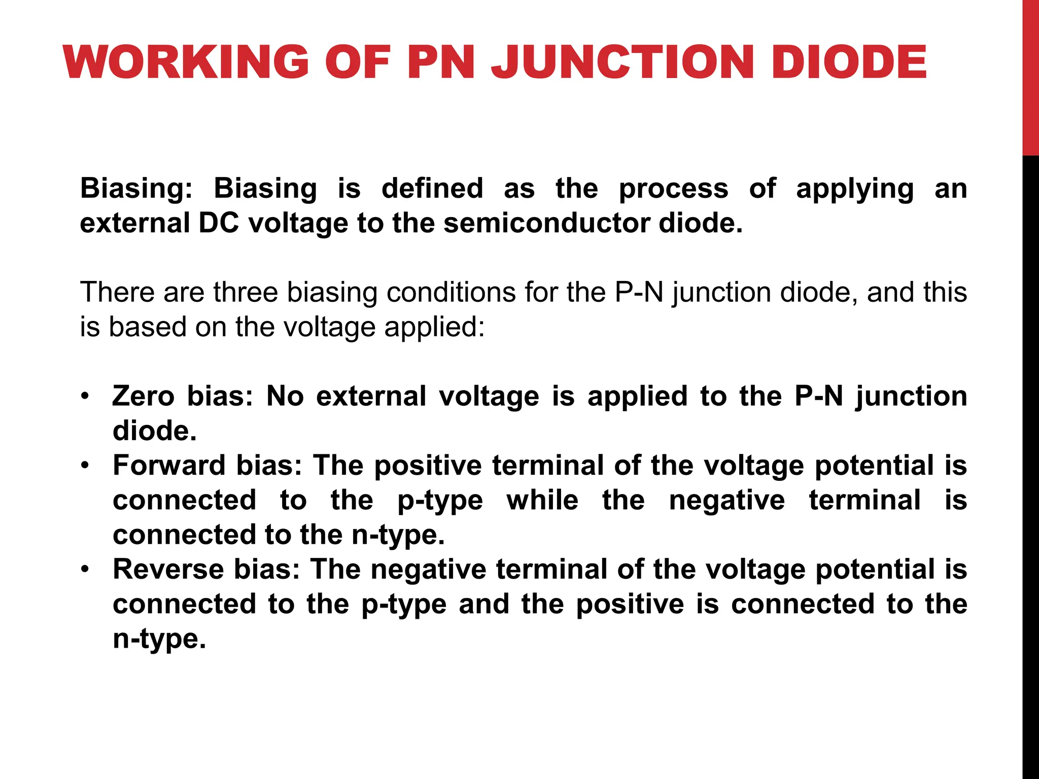
SEMICONDUCTOR AND ITS TYPE
Neeta Ukirade(Gatkal)
Pratibha College of Commerce and
Computer Studies
CONTENTS
• INTRODUCTION
• TYPES OF SEMICONDUCTOR
 INTRINSIC SEMICONDUCTOR
 EXTRINSIC SEMICONDUCTOR
• CARRIER CONCENTRATION
• PN JUNCTION DIODE
INTRODUCTION
 Semiconductors are materials which have a conductivity
between conductors (generally metals) and non-conductors
or insulators (such as ceramics).
 Semiconductors can be compounds, such as gallium
arsenide, or pure elements, such as germanium or silicon.
 Holes and electrons are the types of charge carriers
accountable for the flow of current in semiconductors.
 Holes (valence electrons) are the positively charged
electric charge carrier, whereas electrons are the negatively
charged particles.
 Both electrons and holes are equal in magnitude but
opposite in polarity.
 In a semiconductor, the mobility of electrons is higher than that
of the holes.
 It is mainly because of their different band structures and scattering
mechanisms.
 Electrons travel in the conduction band, whereas holes travel in the
valence band.
 When an electric field is applied, holes cannot move as freely as
electrons due to their restricted movement.
TYPES OF SEMICONDUCTORS
Semiconductors can be classified as follows:
 Intrinsic Semiconductor
 Extrinsic Semiconductor
INTRINSIC SEMICONDUCTOR
 An intrinsic type of semiconductor material is made to be very pure
chemically. It is made up of only a single type of element.
 Germanium (Ge) and silicon (Si) are the most common types of intrinsic
semiconductor elements. They have four valence electrons (tetravalent).
They are bound to the atom by a covalent bond at absolute zero
temperature.
 When the temperature rises due to collisions, few electrons are
unbounded and become free to move through the lattice, thus creating an
absence in its original position (hole).
 These free electrons and holes contribute to the conduction of electricity
in the semiconductor.
EXTRINSIC SEMICONDUCTOR
 The conductivity of semiconductors can be greatly improved by introducing a
small number of suitable replacement atoms called IMPURITIES.
 The process of adding impurity atoms to the pure semiconductor is called
DOPING.
Extrinsic semiconductor can be further classified into types:
 N-type Semiconductor
 P-type Semiconductor
N-TYPE SEMICONDUCTOR
 When a pure semiconductor (silicon or germanium) is doped by pentavalent
impurity (P, As, Sb, Bi), then four electrons out of five valence electrons bond
with the four electrons of Ge or Si.
 The fifth electron of the dopant is set free. Thus, the impurity atom donates a
free electron for conduction in the lattice and is called a “Donar“.
 The number of free electrons increases with the addition of an impurity, the
negative charge carriers increase. Hence, it is called an n-type
semiconductor.
 As conduction is due to a large number of free electrons, the electrons in the
n-type semiconductor are the MAJORITY CARRIERS, and holes are the
MINORITY CARRIERS.
P-TYPE SEMICONDUCTOR
 When a pure semiconductor is doped with a trivalent impurity (B, Al,
In, Ga), then the three valence electrons of the impurity bond with
three of the four valence electrons of the semiconductor.
 This leaves an absence of electron (hole) in the impurity. These
impurity atoms which are ready to accept bonded electrons are
called “Acceptors“.
 With an increase in the number of impurities, holes (the positive
charge carriers) are increased. Hence, it is called a p-type
semiconductor.
PN JUNCTION
 P type and n type semiconductors, taken separately are of limited
use.
 If we join a piece of P type material to a piece of N type material such
that the crystal structure remain continuous at the boundary, a PN
junction is formed.
PN JUNCTION DIODE
A P-N junction is a device formed by joining p-type with n type semiconductor
and separated by a thin junction is called PN junction diode.
Formation of Depletion Layer
 During the formation of p-n junction, the holes diffuse from p-type
semiconductor to the n-type, and electrons diffuse from n-type to p-type.
 When a hole diffuses from p to n type, it leaves an unmovable negative charge.
Similarly, when an electron diffuses from n to p type, it leaves an unmovable
positive charge.
 When the diffusion of holes and electrons takes place continuously across the
junction, a layer of unmovable positive and negative charges are developed on
either side of the junction. This layer is called the depletion layer
 The potential difference across the region is called the barrier potential.
WORKING OF PN JUNCTION DIODE
Biasing: Biasing is defined as the process of applying an
external DC voltage to the semiconductor diode.
There are three biasing conditions for the P-N junction diode, and this
is based on the voltage applied:
• Zero bias: No external voltage is applied to the P-N junction
diode.
• Forward bias: The positive terminal of the voltage potential is
connected to the p-type while the negative terminal is
connected to the n-type.
• Reverse bias: The negative terminal of the voltage potential is
connected to the p-type and the positive is connected to the
n-type.
FORWARD BIASED PN JUNCTION
The p-n junction is said to be forward-biased when the p-
type is connected to the positive terminal of the battery
and the n-type to the negative terminal. The built-in
electric field at the p-n junction and the applied electric
field are in opposing directions when the p-n junction is
forward biased.
REVERSE BIASED PN JUNCTION
The p-n junction is said to be reverse-biased when the p-
type is linked to the negative terminal of the battery and the
n-type is attached to the positive side. The applied electric
field and the built-in electric field are both in the same
direction in this situation.
THANK YOU

Introduction of Semiconductor and Its Type .pptx

  • 1.
    SEMICONDUCTOR AND ITSTYPE Neeta Ukirade(Gatkal) Pratibha College of Commerce and Computer Studies
  • 2.
    CONTENTS • INTRODUCTION • TYPESOF SEMICONDUCTOR  INTRINSIC SEMICONDUCTOR  EXTRINSIC SEMICONDUCTOR • CARRIER CONCENTRATION • PN JUNCTION DIODE
  • 3.
    INTRODUCTION  Semiconductors arematerials which have a conductivity between conductors (generally metals) and non-conductors or insulators (such as ceramics).  Semiconductors can be compounds, such as gallium arsenide, or pure elements, such as germanium or silicon.  Holes and electrons are the types of charge carriers accountable for the flow of current in semiconductors.  Holes (valence electrons) are the positively charged electric charge carrier, whereas electrons are the negatively charged particles.  Both electrons and holes are equal in magnitude but opposite in polarity.
  • 4.
     In asemiconductor, the mobility of electrons is higher than that of the holes.  It is mainly because of their different band structures and scattering mechanisms.  Electrons travel in the conduction band, whereas holes travel in the valence band.  When an electric field is applied, holes cannot move as freely as electrons due to their restricted movement.
  • 5.
    TYPES OF SEMICONDUCTORS Semiconductorscan be classified as follows:  Intrinsic Semiconductor  Extrinsic Semiconductor
  • 6.
    INTRINSIC SEMICONDUCTOR  Anintrinsic type of semiconductor material is made to be very pure chemically. It is made up of only a single type of element.  Germanium (Ge) and silicon (Si) are the most common types of intrinsic semiconductor elements. They have four valence electrons (tetravalent). They are bound to the atom by a covalent bond at absolute zero temperature.  When the temperature rises due to collisions, few electrons are unbounded and become free to move through the lattice, thus creating an absence in its original position (hole).  These free electrons and holes contribute to the conduction of electricity in the semiconductor.
  • 7.
    EXTRINSIC SEMICONDUCTOR  Theconductivity of semiconductors can be greatly improved by introducing a small number of suitable replacement atoms called IMPURITIES.  The process of adding impurity atoms to the pure semiconductor is called DOPING. Extrinsic semiconductor can be further classified into types:  N-type Semiconductor  P-type Semiconductor
  • 9.
    N-TYPE SEMICONDUCTOR  Whena pure semiconductor (silicon or germanium) is doped by pentavalent impurity (P, As, Sb, Bi), then four electrons out of five valence electrons bond with the four electrons of Ge or Si.  The fifth electron of the dopant is set free. Thus, the impurity atom donates a free electron for conduction in the lattice and is called a “Donar“.  The number of free electrons increases with the addition of an impurity, the negative charge carriers increase. Hence, it is called an n-type semiconductor.  As conduction is due to a large number of free electrons, the electrons in the n-type semiconductor are the MAJORITY CARRIERS, and holes are the MINORITY CARRIERS.
  • 10.
    P-TYPE SEMICONDUCTOR  Whena pure semiconductor is doped with a trivalent impurity (B, Al, In, Ga), then the three valence electrons of the impurity bond with three of the four valence electrons of the semiconductor.  This leaves an absence of electron (hole) in the impurity. These impurity atoms which are ready to accept bonded electrons are called “Acceptors“.  With an increase in the number of impurities, holes (the positive charge carriers) are increased. Hence, it is called a p-type semiconductor.
  • 11.
    PN JUNCTION  Ptype and n type semiconductors, taken separately are of limited use.  If we join a piece of P type material to a piece of N type material such that the crystal structure remain continuous at the boundary, a PN junction is formed.
  • 12.
    PN JUNCTION DIODE AP-N junction is a device formed by joining p-type with n type semiconductor and separated by a thin junction is called PN junction diode. Formation of Depletion Layer  During the formation of p-n junction, the holes diffuse from p-type semiconductor to the n-type, and electrons diffuse from n-type to p-type.  When a hole diffuses from p to n type, it leaves an unmovable negative charge. Similarly, when an electron diffuses from n to p type, it leaves an unmovable positive charge.  When the diffusion of holes and electrons takes place continuously across the junction, a layer of unmovable positive and negative charges are developed on either side of the junction. This layer is called the depletion layer  The potential difference across the region is called the barrier potential.
  • 13.
    WORKING OF PNJUNCTION DIODE Biasing: Biasing is defined as the process of applying an external DC voltage to the semiconductor diode. There are three biasing conditions for the P-N junction diode, and this is based on the voltage applied: • Zero bias: No external voltage is applied to the P-N junction diode. • Forward bias: The positive terminal of the voltage potential is connected to the p-type while the negative terminal is connected to the n-type. • Reverse bias: The negative terminal of the voltage potential is connected to the p-type and the positive is connected to the n-type.
  • 14.
    FORWARD BIASED PNJUNCTION The p-n junction is said to be forward-biased when the p- type is connected to the positive terminal of the battery and the n-type to the negative terminal. The built-in electric field at the p-n junction and the applied electric field are in opposing directions when the p-n junction is forward biased.
  • 15.
    REVERSE BIASED PNJUNCTION The p-n junction is said to be reverse-biased when the p- type is linked to the negative terminal of the battery and the n-type is attached to the positive side. The applied electric field and the built-in electric field are both in the same direction in this situation.
  • 16.