The document discusses the fundamentals of semiconductor materials and devices. It covers topics such as silicon crystal structure, doping, energy bands, carrier concentrations, and the Fermi level. Key points include:
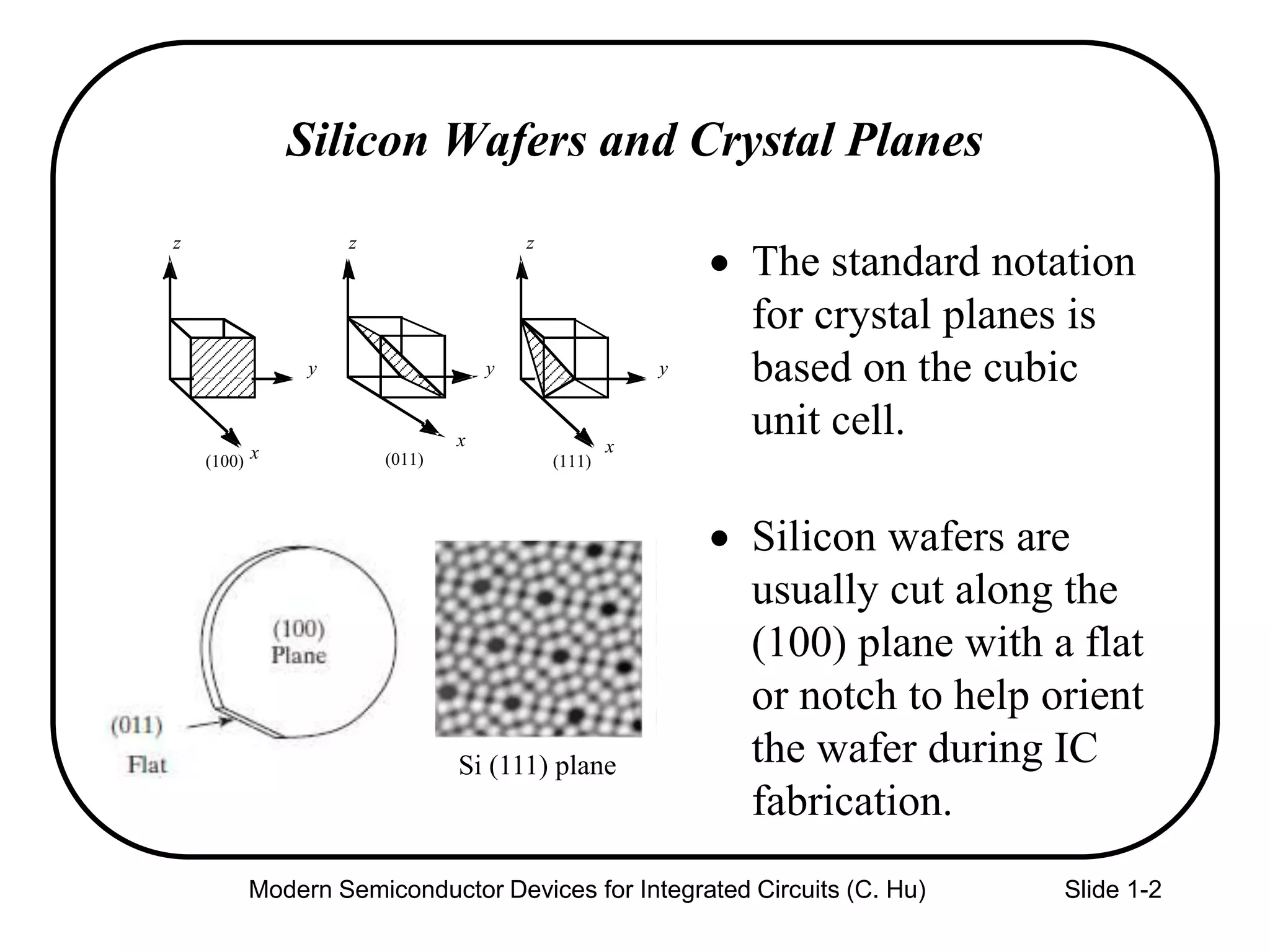
- Silicon crystals have a cubic unit cell structure with each silicon atom bonded to four nearest neighbors. Silicon wafers are cut along specific crystal planes for integrated circuit fabrication.
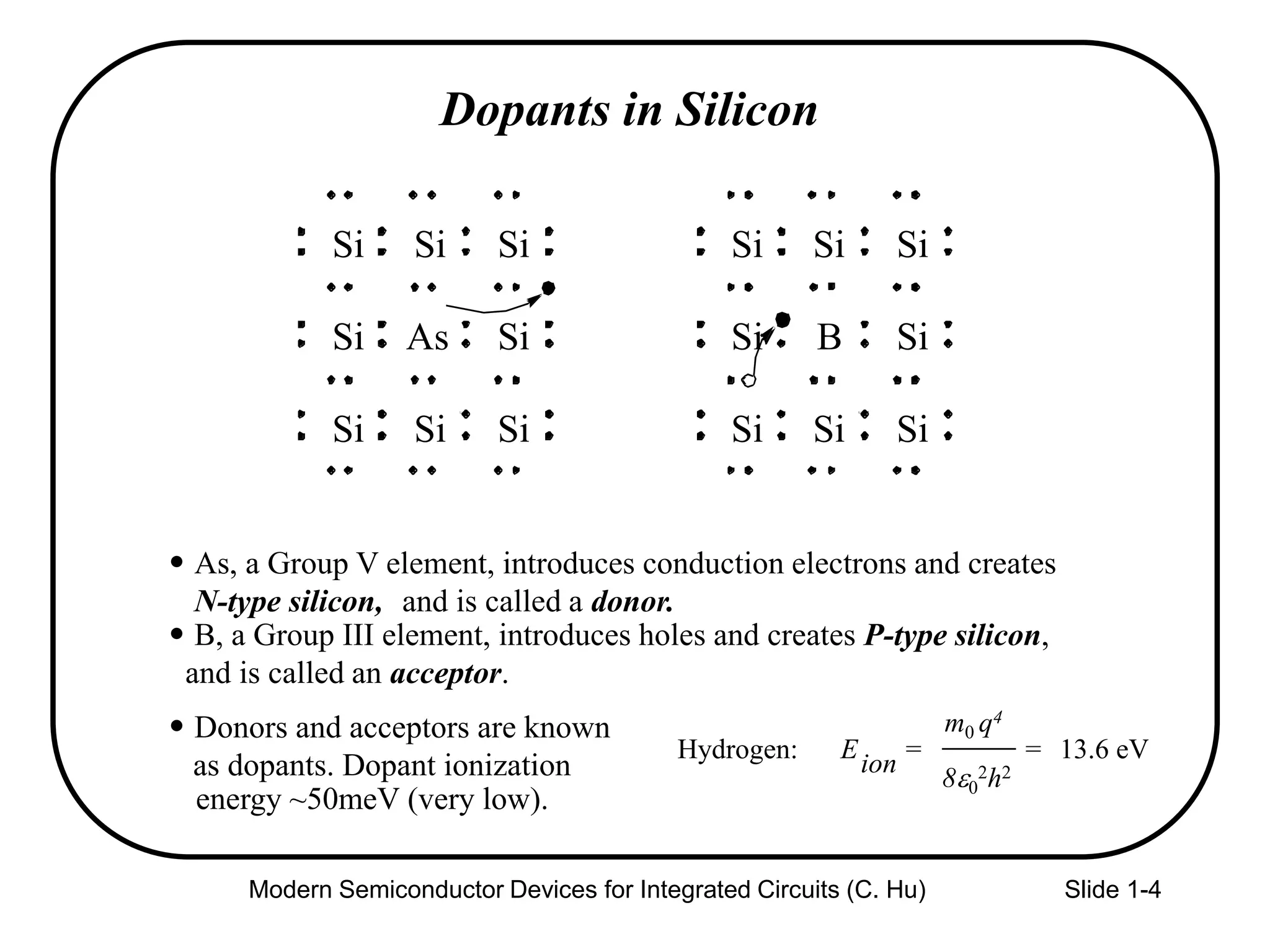
- Doping silicon with elements from columns III and V of the periodic table creates N-type and P-type materials by introducing extra electrons or holes. This allows the control of carrier concentrations.
- The energy band model describes the transition from discrete atomic energy levels to continuous energy bands in solids. The sizes of the bandgap
Modern Semiconductor Devicesfor Integrated Circuits (C. Hu) Slide 1-1
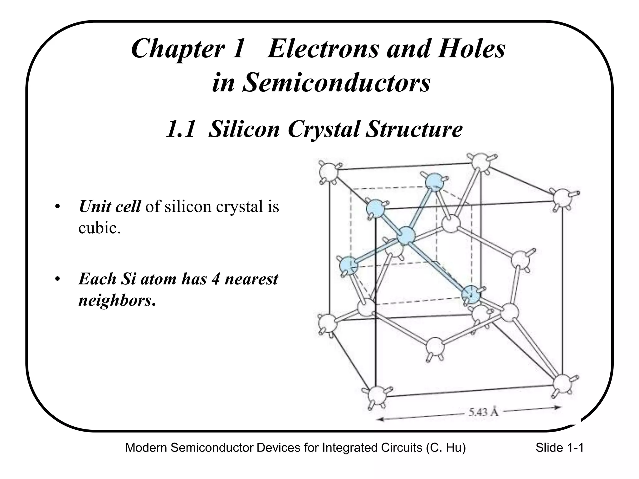
1.1 Silicon Crystal Structure
• Unit cell of silicon crystal is
cubic.
• Each Si atom has 4 nearest
neighbors.
Chapter 1 Electrons and Holes
in Semiconductors
2.
Modern Semiconductor Devicesfor Integrated Circuits (C. Hu) Slide 1-2
Silicon Wafers and Crystal Planes
Silicon wafers are
usually cut along the
(100) plane with a flat
or notch to help orient
the wafer during IC
fabrication.
The standard notation
for crystal planes is
based on the cubic
unit cell.
(100) (011) (111)x
y y y
z z z
x x
Si (111) plane
3.
Modern Semiconductor Devicesfor Integrated Circuits (C. Hu) Slide 1-3
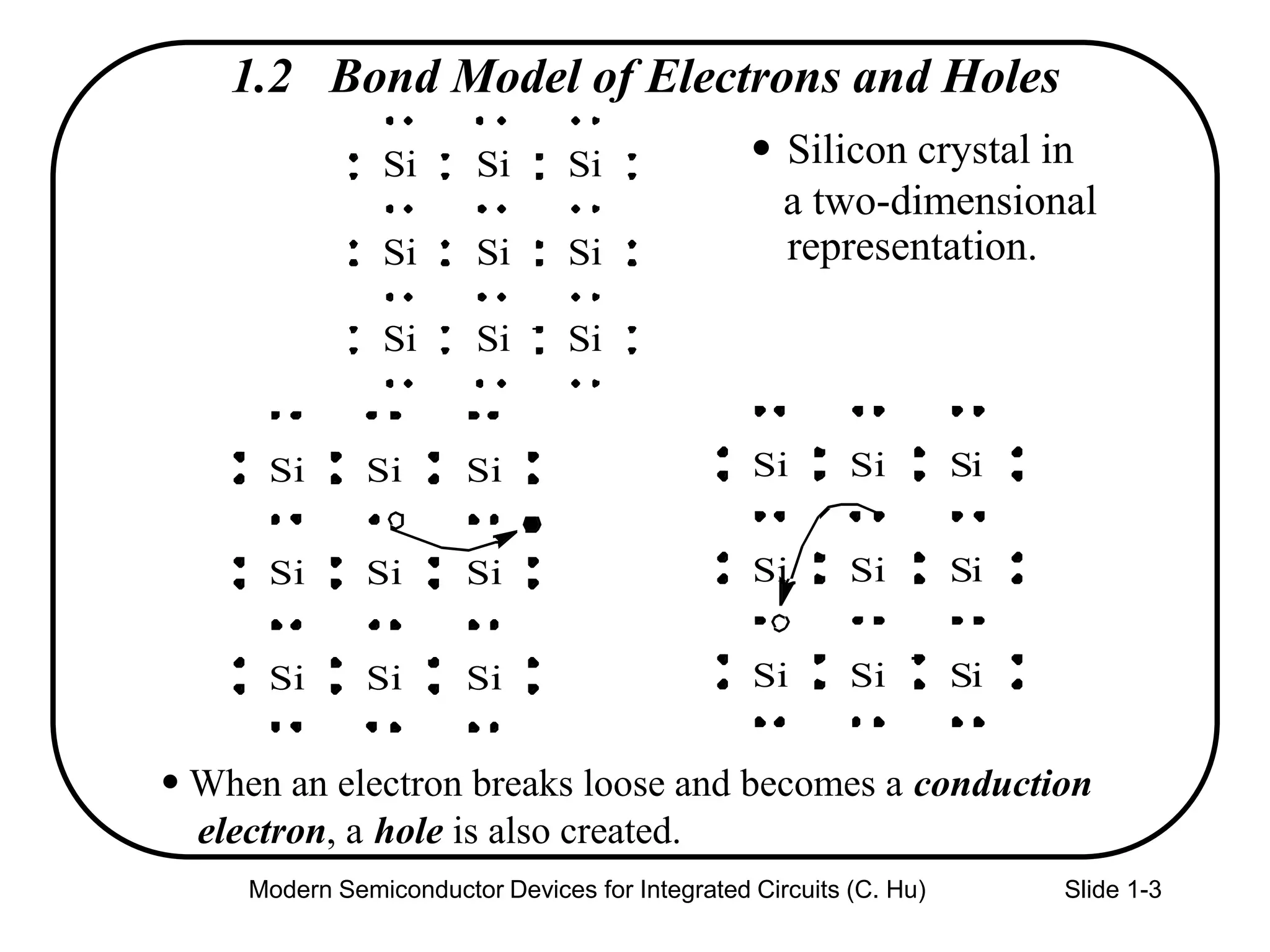
1.2 Bond Model of Electrons and Holes
Silicon crystal in
a two-dimensional
representation.
Si Si Si
Si Si Si
Si Si Si
When an electron breaks loose and becomes a conduction
electron, a hole is also created.
(a) (b)
Si Si Si
Si Si Si
Si Si Si
Si Si Si
Si Si Si
Si Si Si
4.
Modern Semiconductor Devicesfor Integrated Circuits (C. Hu) Slide 1-4
Dopants in Silicon
Si Si Si
Si Si
Si Si Si
Si Si Si
Si Si
Si Si Si
As B
As, a Group V element, introduces conduction electrons and creates
N-type silicon,
B, a Group III element, introduces holes and creates P-type silicon,
and is called an acceptor.
Donors and acceptors are known
as dopants. Dopant ionization
energy ~50meV (very low).
and is called a donor.
Hydrogen: E
ion
m0 q4
13.6 eV==
8e0
2h2
5.
Modern Semiconductor Devicesfor Integrated Circuits (C. Hu) Slide 1-5
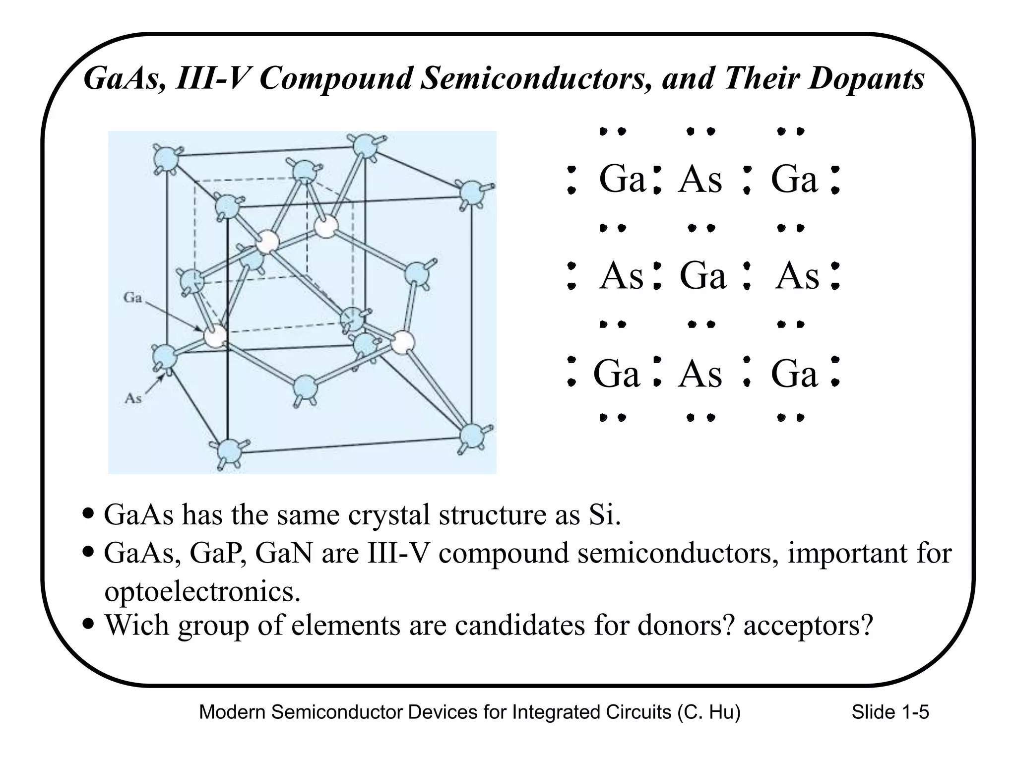
GaAs, III-V Compound Semiconductors, and Their Dopants
As AsGa
Ga
GaAs has the same crystal structure as Si.
GaAs, GaP, GaN are III-V compound semiconductors, important for
optoelectronics.
Wich group of elements are candidates for donors? acceptors?
GaAs
AsGa Ga
6.
Modern Semiconductor Devicesfor Integrated Circuits (C. Hu) Slide 1-6
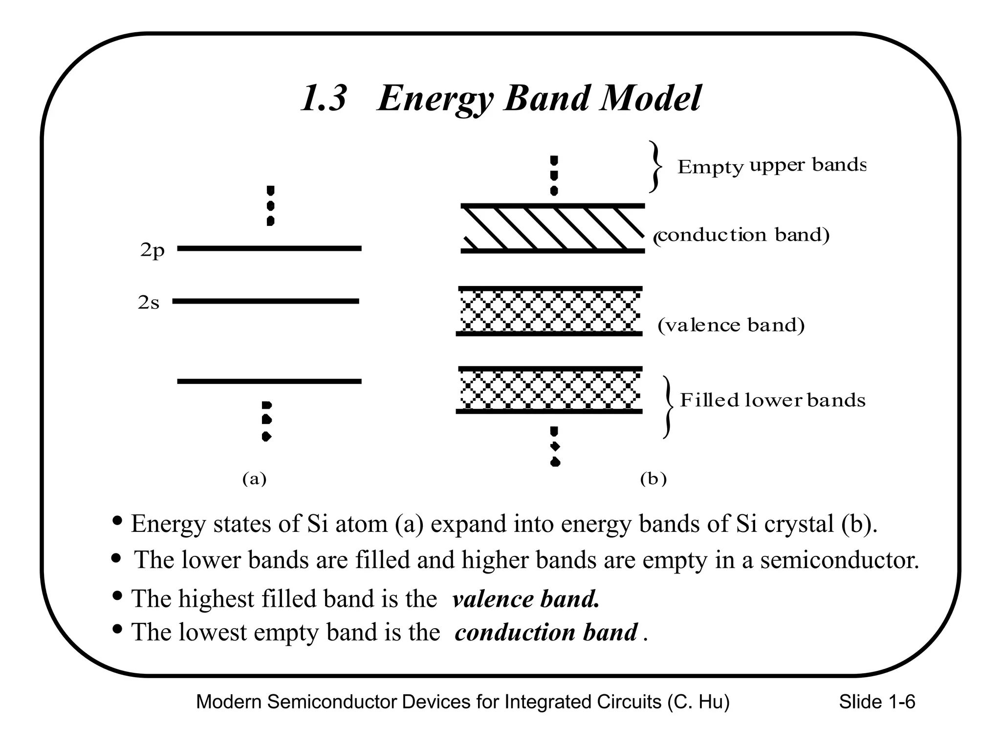
1.3 Energy Band Model
Energy states of Si atom (a) expand into energy bands of Si crystal (b).
The lower bands are filled and higher bands are empty in a semiconductor.
The highest filled band is the valence band.
The lowest empty band is the conduction band .
2p
2s
(a) (b)
conduction band)(
(valence band)
Filled lower bands
} Empty upper bands
}
7.
Modern Semiconductor Devicesfor Integrated Circuits (C. Hu) Slide 1-7
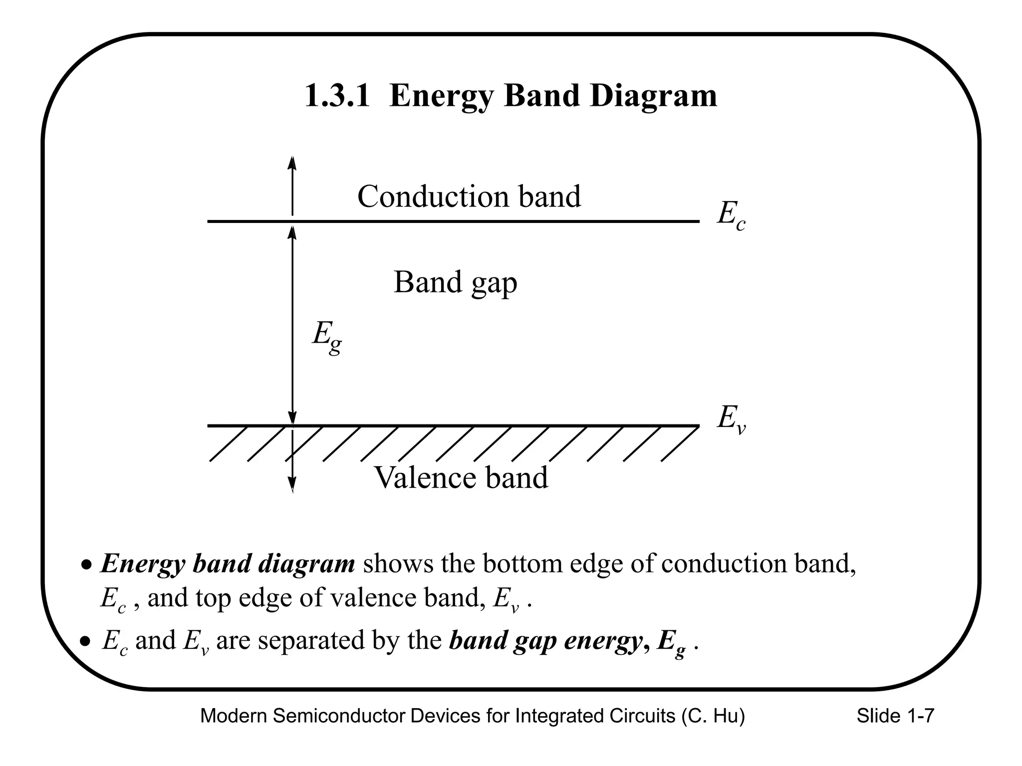
1.3.1 Energy Band Diagram
Conduction band Ec
Ev
Eg
Band gap
Valence band
Energy band diagram shows the bottom edge of conduction band,
Ec , and top edge of valence band, Ev .
Ec and Ev are separated by the band gap energy, Eg .
8.
Modern Semiconductor Devicesfor Integrated Circuits (C. Hu) Slide 1-8
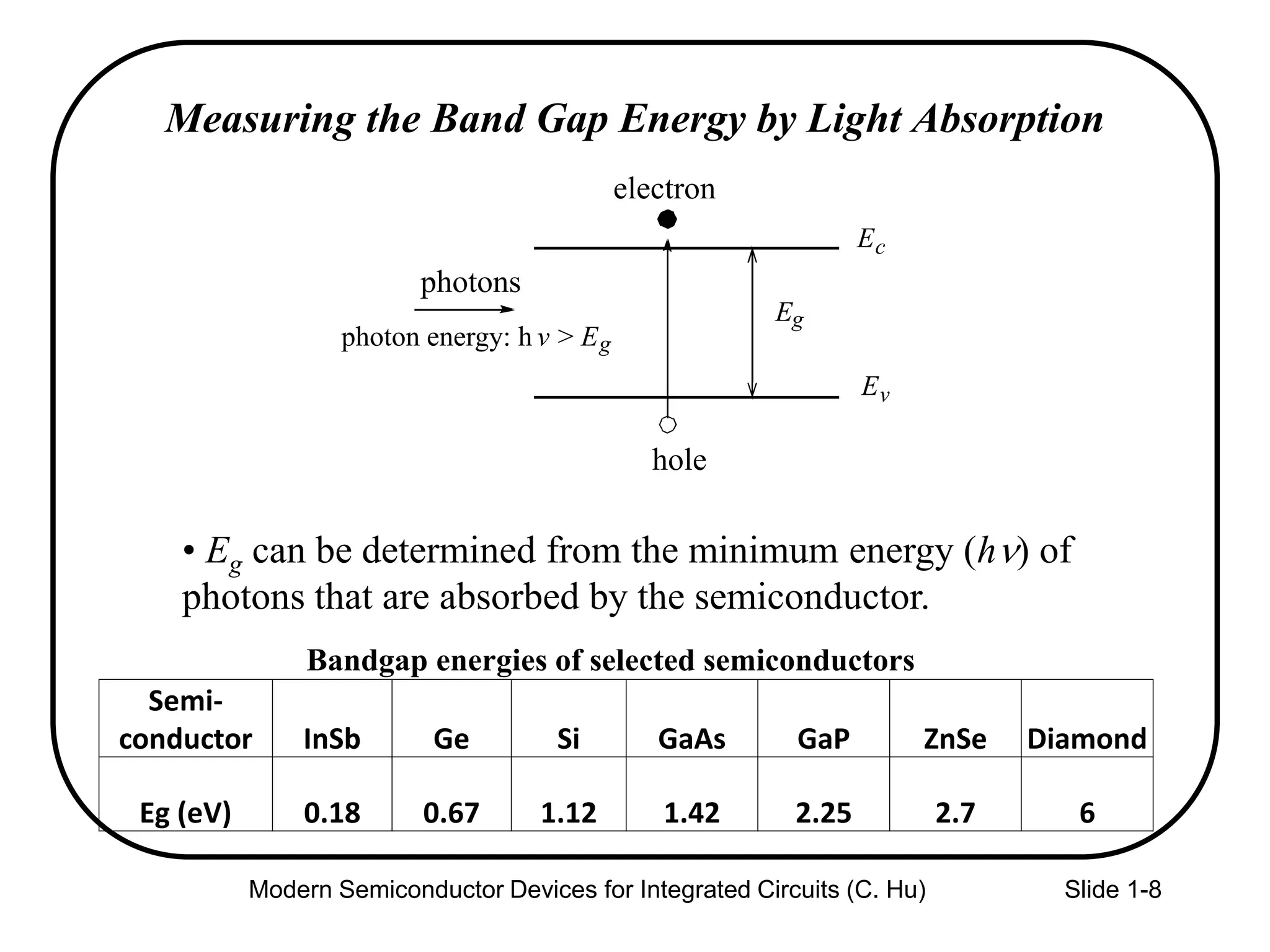
Measuring the Band Gap Energy by Light Absorption
photons
photon energy: h v > Eg
Ec
Ev
Eg
electron
hole
Bandgap energies of selected semiconductors
• Eg can be determined from the minimum energy (hn) of
photons that are absorbed by the semiconductor.
Semi-
conductor InSb Ge Si GaAs GaP ZnSe Diamond
Eg (eV) 0.18 0.67 1.12 1.42 2.25 2.7 6
9.
Modern Semiconductor Devicesfor Integrated Circuits (C. Hu) Slide 1-9
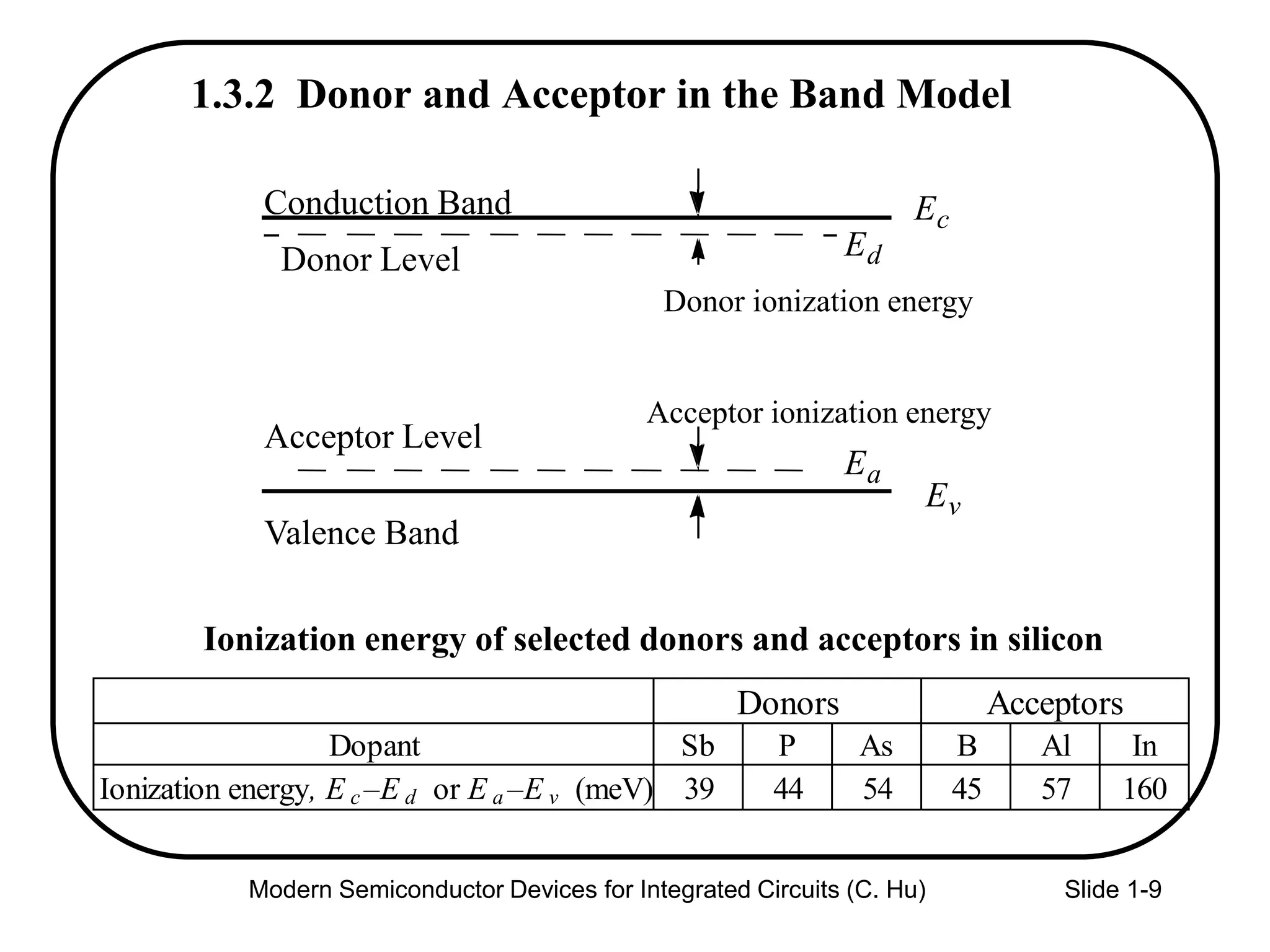
1.3.2 Donor and Acceptor in the Band Model
Conduction Band Ec
Ev
Valence Band
Donor Level
Acceptor Level
Ed
Ea
Donor ionization energy
Acceptor ionization energy
Ionization energy of selected donors and acceptors in silicon
Acceptors
Dopant Sb P As B Al In
Ionization energy, E c –E d or E a –E v (meV) 39 44 54 45 57 160
Donors
10.
Modern Semiconductor Devicesfor Integrated Circuits (C. Hu) Slide 1-10
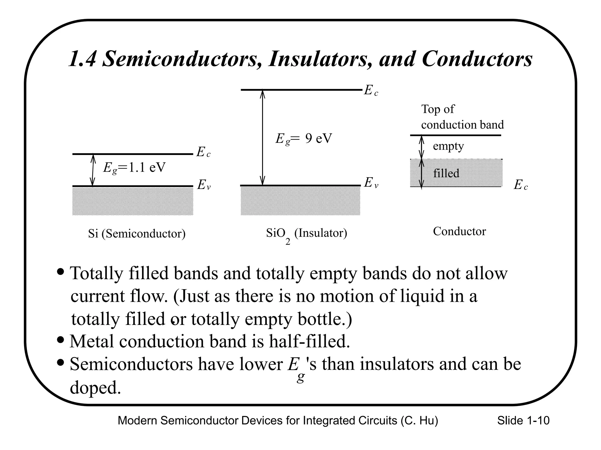
1.4 Semiconductors, Insulators, and Conductors
Totally filled bands and totally empty bands do not allow
Metal conduction band is half-filled.
Ec
Ev
Eg=1.1 eV
Ec
Eg= 9 eV empty
Si (Semiconductor) SiO
2
(Insulator) Conductor
Ec
filled
Top of
conduction band
Ev
current flow. (Just as there is no motion of liquid in a
totally filled or totally empty bottle.).
Semiconductors have lower E
g
's than insulators and can be
doped.
11.
Modern Semiconductor Devicesfor Integrated Circuits (C. Hu) Slide 1-11
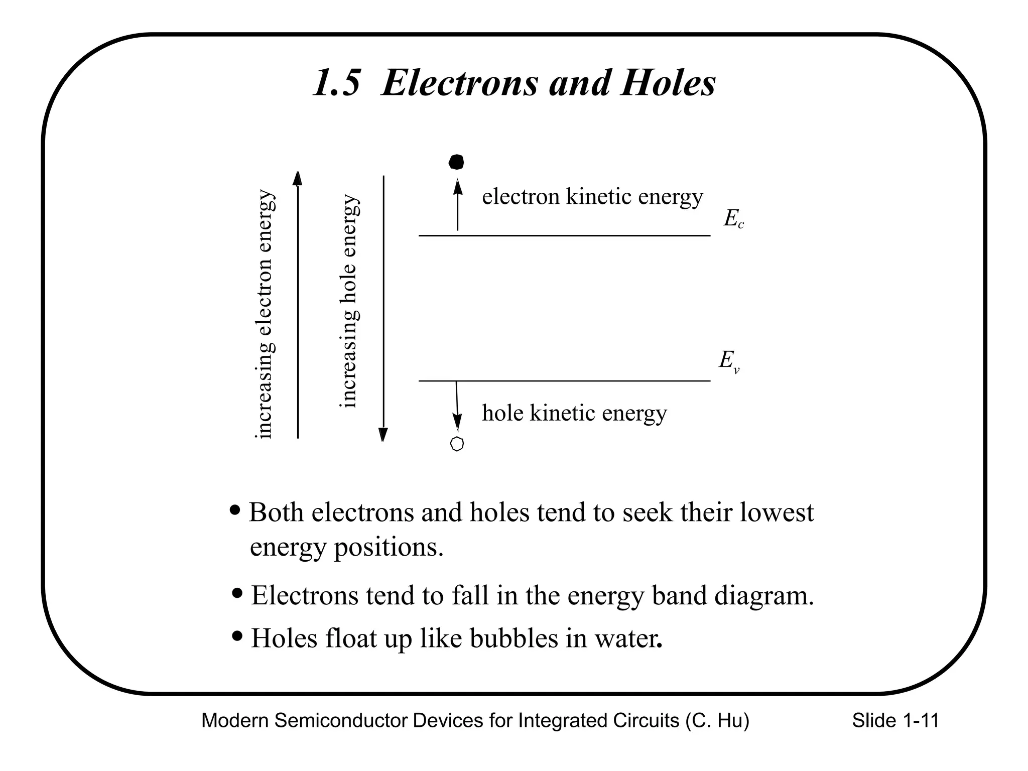
1.5 Electrons and Holes
Both electrons and holes tend to seek their lowest
Holes float up like bubbles in water.
Electrons tend to fall in the energy band diagram.
Ec
Ev
electron kinetic energy
hole kinetic energy
increasingelectronenergy
increasingholeenergy
energy positions.
12.
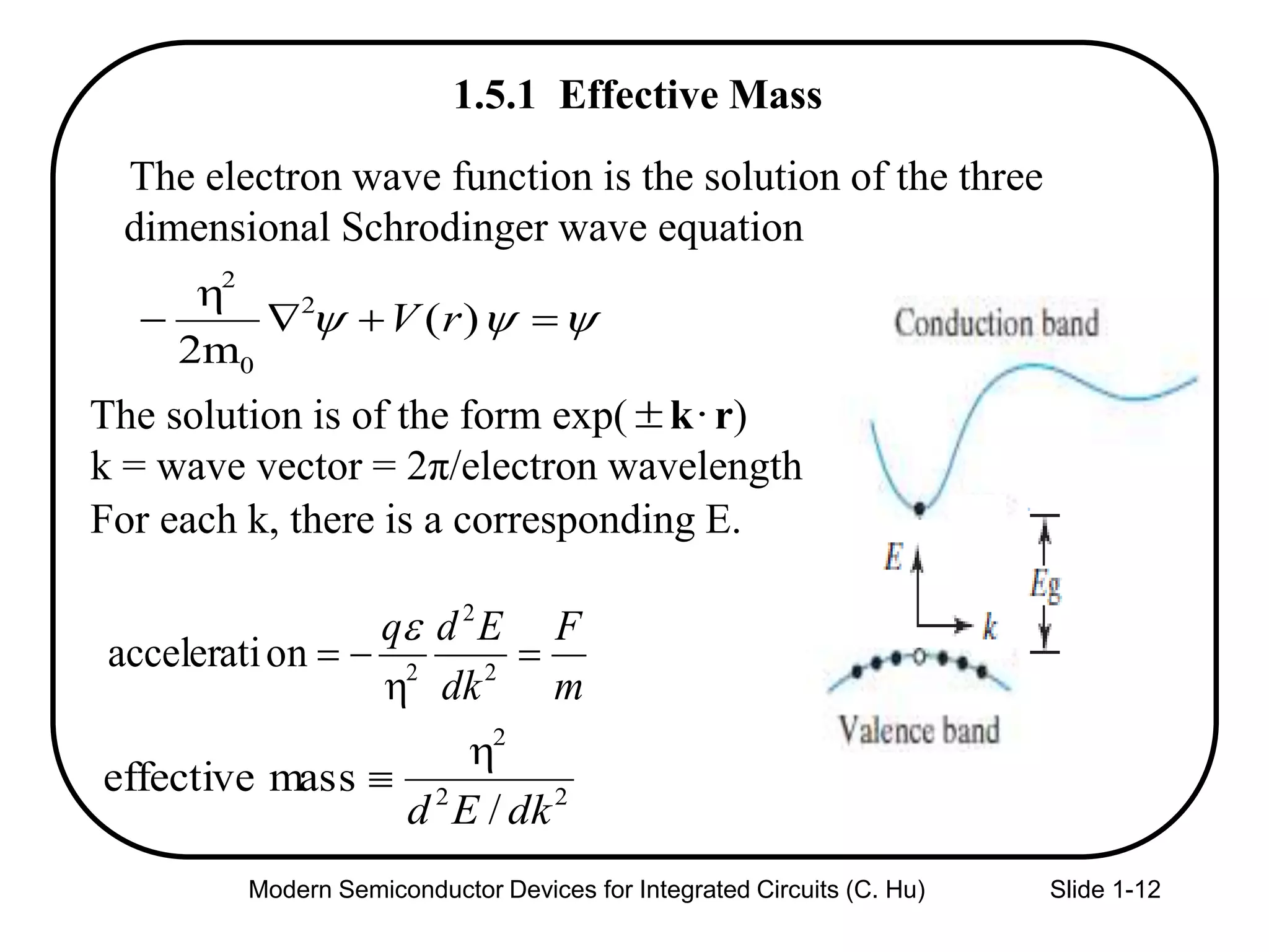
The electron wavefunction is the solution of the three
dimensional Schrodinger wave equation
Modern Semiconductor Devices for Integrated Circuits (C. Hu) Slide 1-12
)(
2m
2
0
2
rV
The solution is of the form exp( k r)
k = wave vector = 2π/electron wavelength
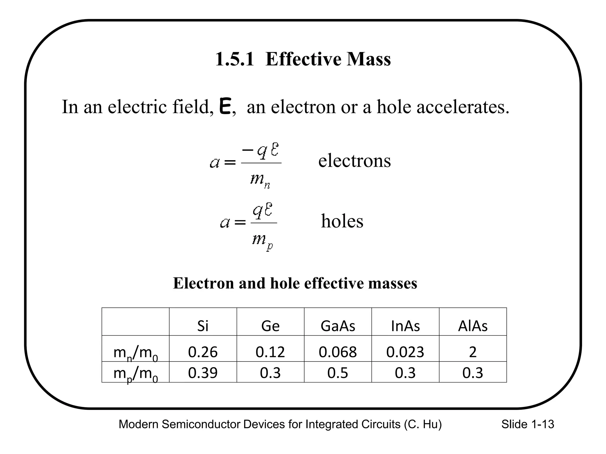
1.5.1 Effective Mass
m
F
dk
Edq
2
2
2
onaccelerati
e
22
2
/
masseffective
dkEd
For each k, there is a corresponding E.
13.
Modern Semiconductor Devicesfor Integrated Circuits (C. Hu) Slide 1-13
1.5.1 Effective Mass
In an electric field, E, an electron or a hole accelerates.
Electron and hole effective masses
electrons
holes
Si Ge GaAs InAs AlAs
mn/m0 0.26 0.12 0.068 0.023 2
mp/m0 0.39 0.3 0.5 0.3 0.3
14.
Modern Semiconductor Devicesfor Integrated Circuits (C. Hu) Slide 1-14
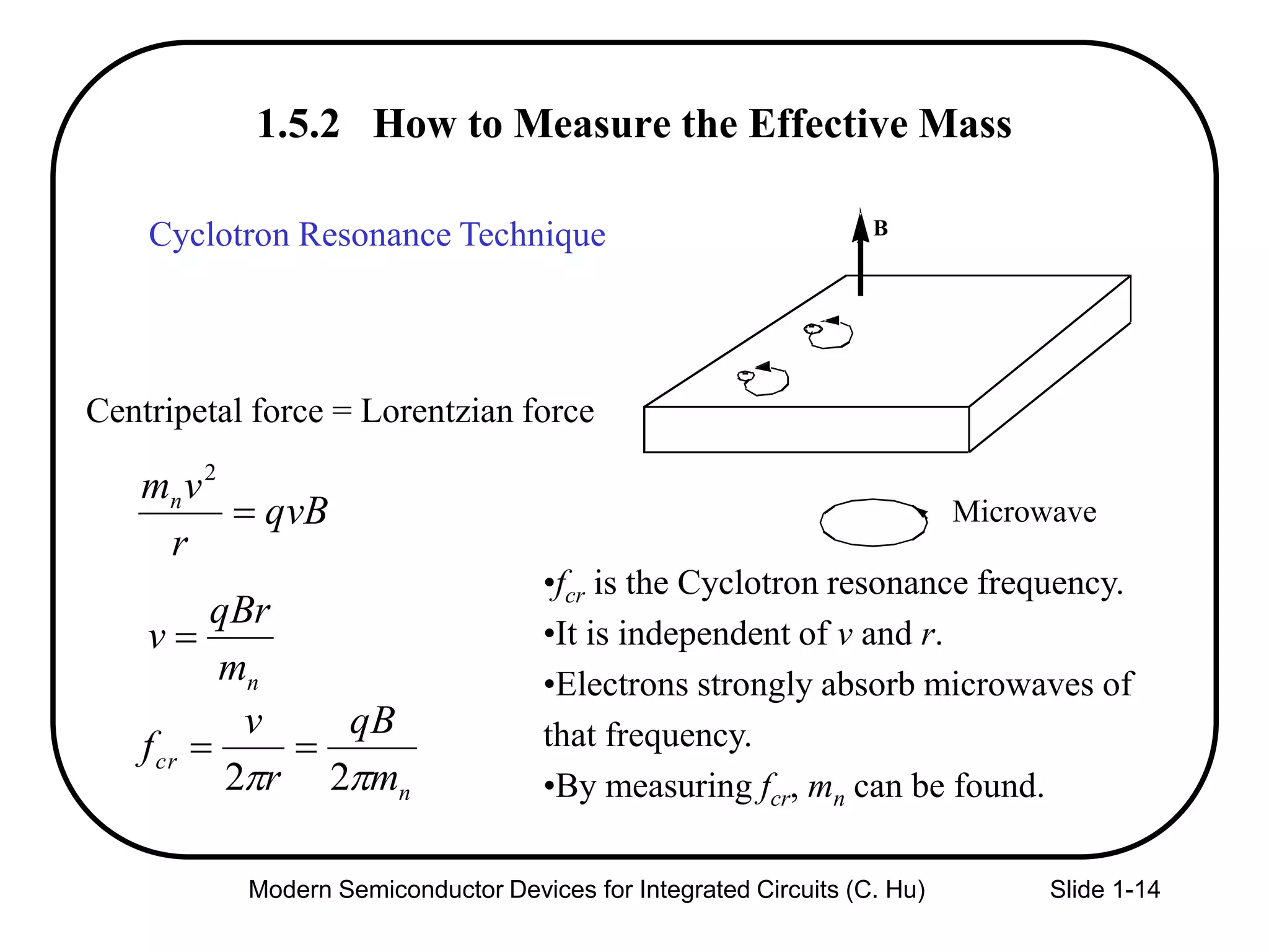
1.5.2 How to Measure the Effective Mass
Cyclotron Resonance Technique
Centripetal force = Lorentzian force
B
-
--
Microwave
•fcr is the Cyclotron resonance frequency.
•It is independent of v and r.
•Electrons strongly absorb microwaves of
that frequency.
•By measuring fcr, mn can be found.
qvB
r
vmn
2
nm
qBr
v
n
cr
m
qB
r
v
f
22
15.
Modern Semiconductor Devicesfor Integrated Circuits (C. Hu) Slide 1-15
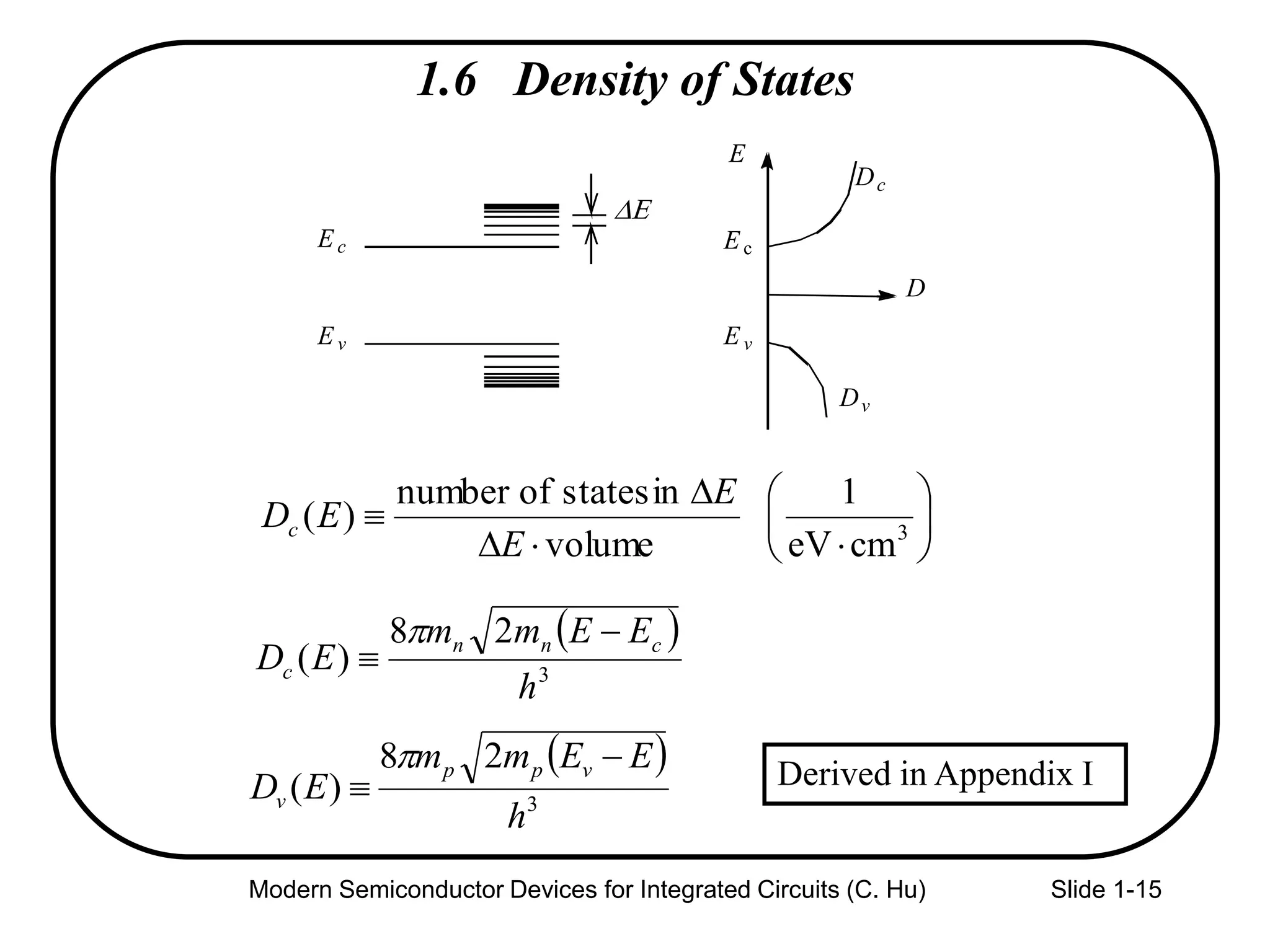
1.6 Density of States
E
Dc
Dv
Ec
Ev
D
Ec
Ev
DE
D
D
3
cmeV
1
volume
instatesofnumber
)(
E
E
EDc
28
)( 3
h
EEmm
ED cnn
c
28
)( 3
h
EEmm
ED
vpp
v
Derived in Appendix I
16.
Modern Semiconductor Devicesfor Integrated Circuits (C. Hu) Slide 1-16
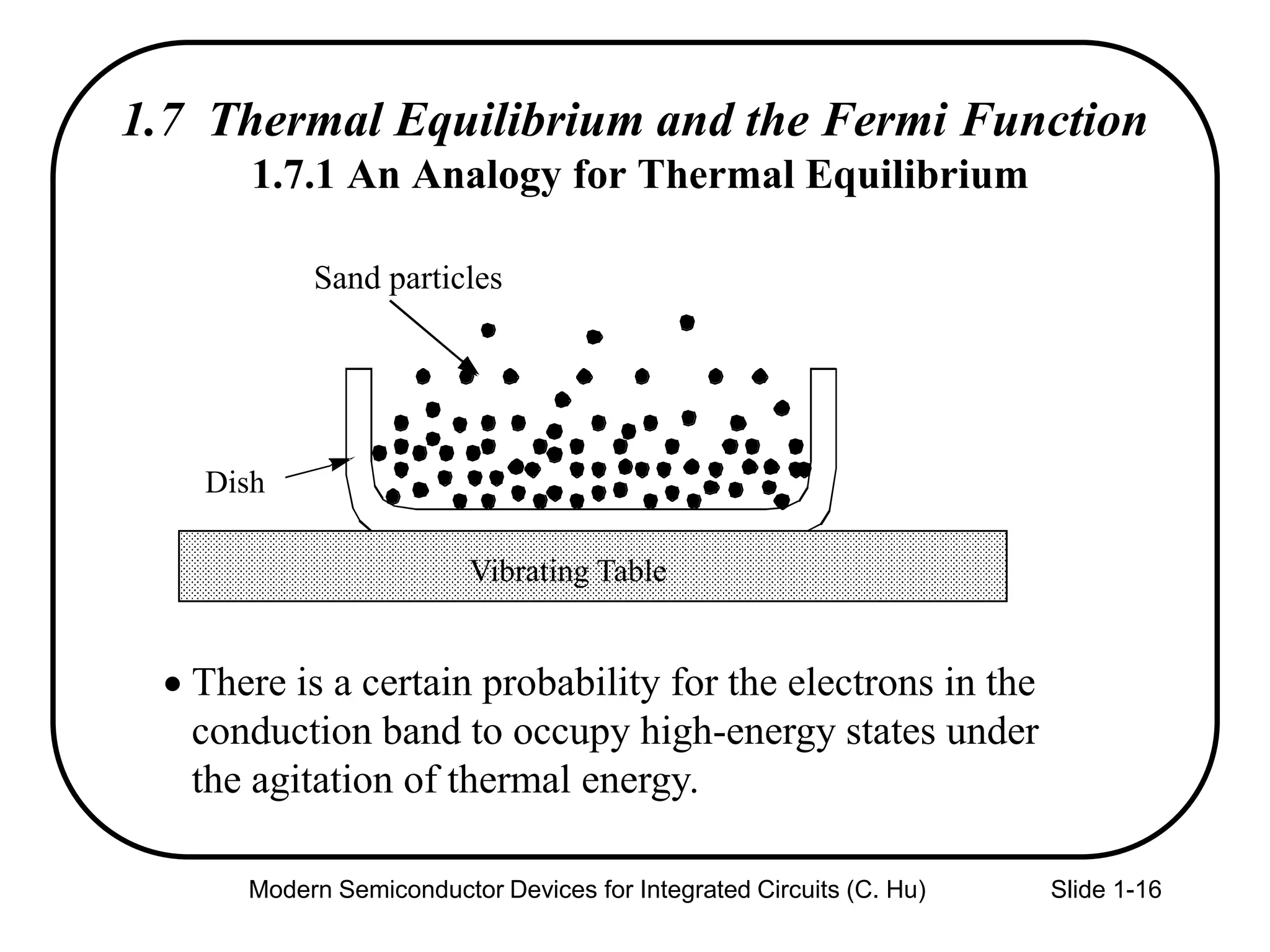
1.7 Thermal Equilibrium and the Fermi Function
1.7.1 An Analogy for Thermal Equilibrium
There is a certain probability for the electrons in the
conduction band to occupy high-energy states under
the agitation of thermal energy.
Dish
Vibrating Table
Sand particles
17.
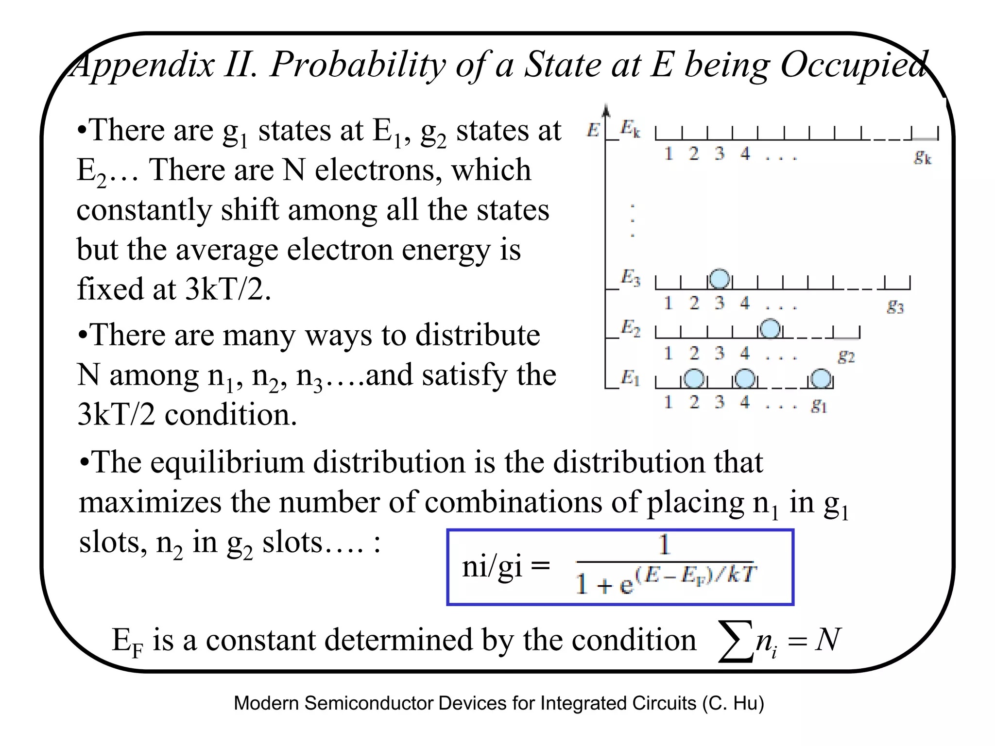
Appendix II. Probabilityof a State at E being Occupied
•There are g1 states at E1, g2 states at
E2… There are N electrons, which
constantly shift among all the states
but the average electron energy is
fixed at 3kT/2.
•The equilibrium distribution is the distribution that
maximizes the number of combinations of placing n1 in g1
slots, n2 in g2 slots…. :
•There are many ways to distribute
N among n1, n2, n3….and satisfy the
3kT/2 condition.
ni/gi =
EF is a constant determined by the condition Nni
Modern Semiconductor Devices for Integrated Circuits (C. Hu)
18.
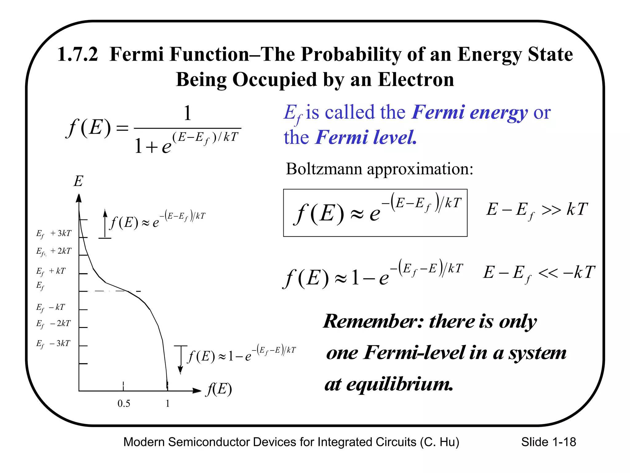
Modern Semiconductor Devicesfor Integrated Circuits (C. Hu) Slide 1-18
1.7.2 Fermi Function–The Probability of an Energy State
Being Occupied by an Electron
Remember: there is only
one Fermi-level in a system
at equilibrium.
kTEE f
e
Ef /)(
1
1
)(
Ef is called the Fermi energy or
the Fermi level.
kTEE f
eEf
)( kTEE f
kTEE f
eEf
1)( kTEE f
Boltzmann approximation:
f(E)
0.5 1
Ef
Ef – kT
Ef – 2kT
Ef – 3kT
Ef + kT
E
f
Ef + 2kT
Ef + 3kT
E
kTEE f
eEf
)(
kTEE f
eEf
1)(
19.
Modern Semiconductor Devicesfor Integrated Circuits (C. Hu) Slide 1-19
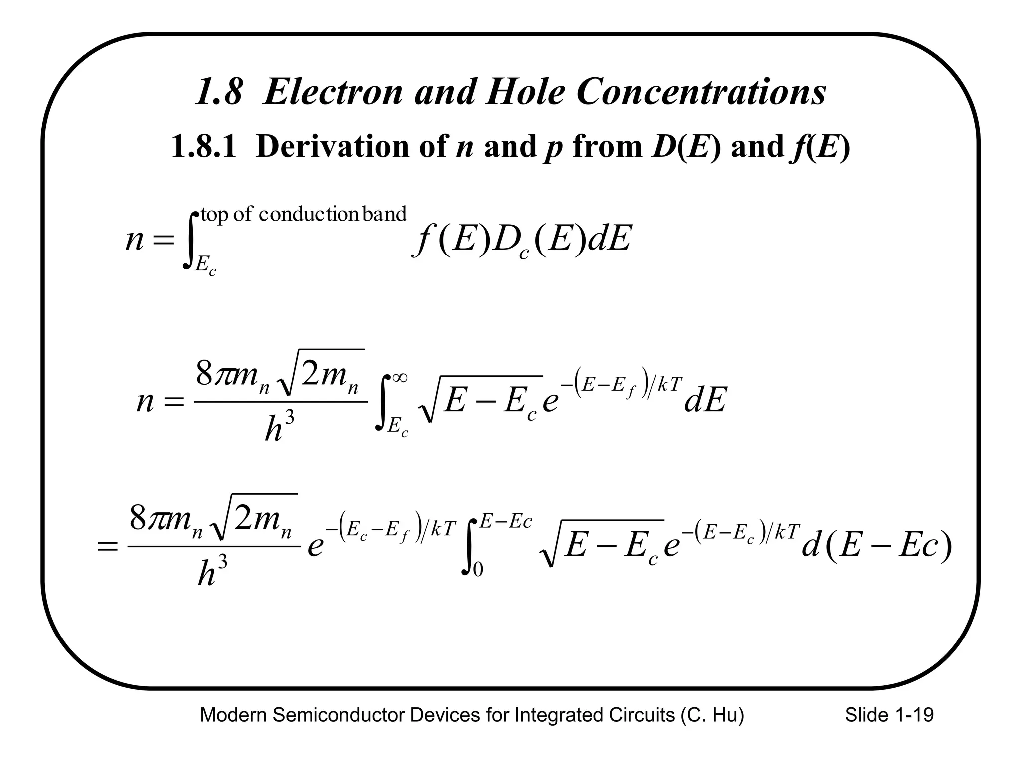
1.8 Electron and Hole Concentrations
bandconductionoftop
)()(
cE
c dEEDEfn
)(
28
03
EcEdeEEe
h
mm kTEE
EcE
c
kTEEnn cfc
dEeEE
h
mm
n
kTEE
E
c
nn f
c
3
28
1.8.1 Derivation of n and p from D(E) and f(E)
20.
Modern Semiconductor Devicesfor Integrated Circuits (C. Hu) Slide 1-20
Electron and Hole Concentrations
Remember: the closer Ef moves up to Nc, the larger n is;
the closer Ef moves down to Ev , the larger p is.
For Si, Nc = 2.8 ´1019
cm-3
and Nv = 1.04´1019
cm-3
.
kTEE
c
fc
eNn
/)(
23
2
2
2
h
kTm
N n
c
kTEE
v
vf
eNp
/)(
23
2
2
2
h
kTm
N
p
v
Nc is called the effective
density of states (of the
conduction band) .
Nv is called the effective
density of states of the
valence band.
21.
Modern Semiconductor Devicesfor Integrated Circuits (C. Hu) Slide 1-21
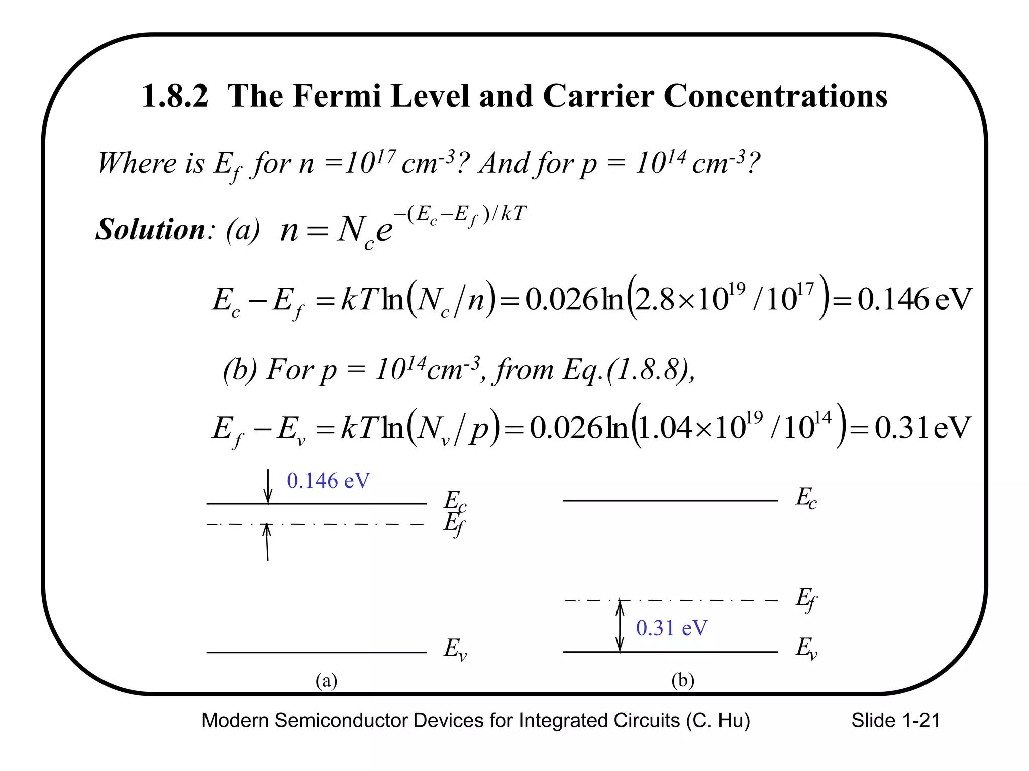
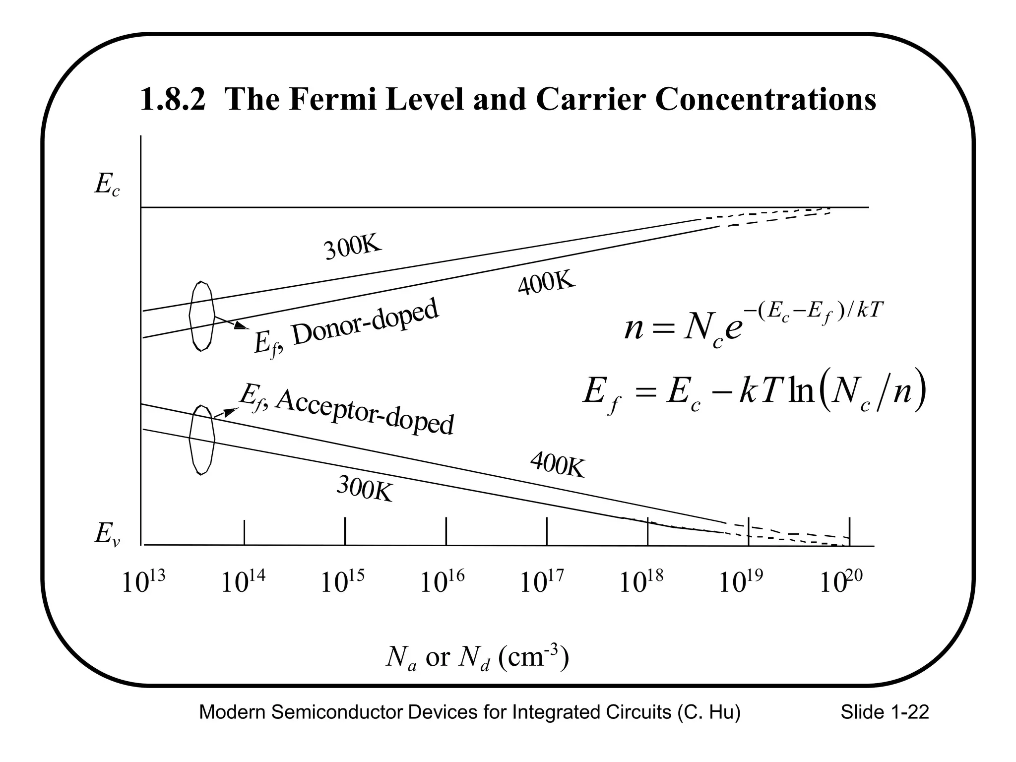
1.8.2 The Fermi Level and Carrier Concentrations
kTEE
c
fc
eNn
/)(
eV614.010/108.2ln026.0ln 1719
nNkTEE cfc
eV31.010/1004.1ln026.0ln 1419
pNkTEE vvf
Ec
Ef
Ev
0.146 eV
(a)
0.31 eV
Ec
Ef
Ev
(b)
Where is Ef for n =1017 cm-3? And for p = 1014 cm-3?
Solution: (a)
(b) For p = 1014cm-3, from Eq.(1.8.8),
22.
Modern Semiconductor Devicesfor Integrated Circuits (C. Hu) Slide 1-22
1.8.2 The Fermi Level and Carrier Concentrations
1013
1014
1015
1016
1017
1018
1019
1020
Ev
Ec
Na or Nd (cm-3
)
kTEE
c
fc
eNn
/)(
nNkTEE ccf ln
23.
Modern Semiconductor Devicesfor Integrated Circuits (C. Hu) Slide 1-23
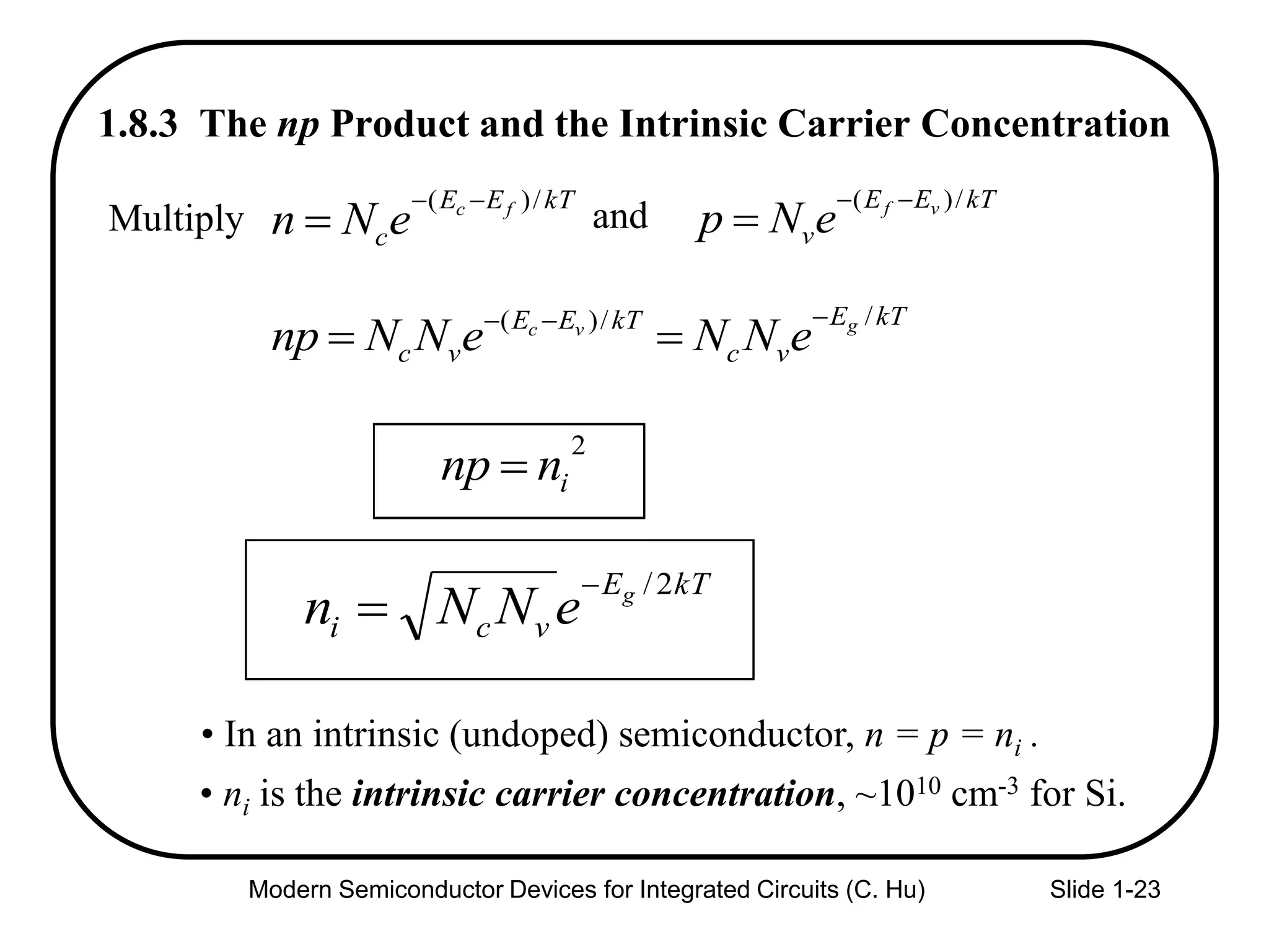
1.8.3 The np Product and the Intrinsic Carrier Concentration
• In an intrinsic (undoped) semiconductor, n = p = ni .
kTE
vci
g
eNNn
2/
2
innp
kTEE
c
fc
eNn
/)(
kTEE
v
vf
eNp
/)(
andMultiply
kTE
vc
kTEE
vc
gvc
eNNeNNnp
//)(
• ni is the intrinsic carrier concentration, ~1010 cm-3 for Si.
24.
Modern Semiconductor Devicesfor Integrated Circuits (C. Hu) Slide 1-24
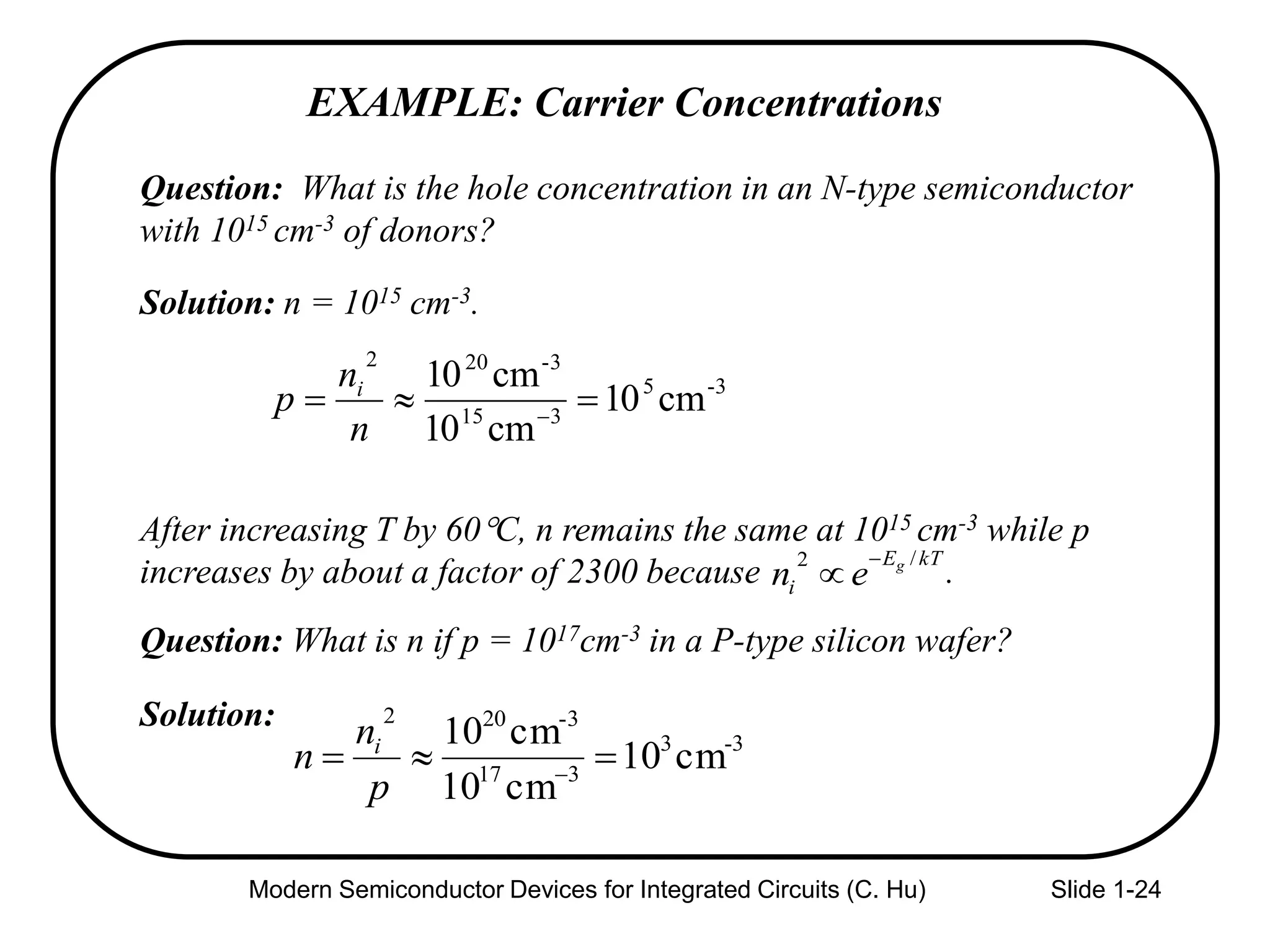
Question: What is the hole concentration in an N-type semiconductor
with 1015 cm-3 of donors?
Solution: n = 1015 cm-3.
After increasing T by 60C, n remains the same at 1015 cm-3 while p
increases by about a factor of 2300 because .
Question: What is n if p = 1017cm-3 in a P-type silicon wafer?
Solution:
EXAMPLE: Carrier Concentrations
3-5
315
-3202
cm10
cm10
cm10
n
n
p i
kTE
i
g
en
/2
3-3
317
-3202
cm10
cm10
cm10
p
n
n i
25.
Modern Semiconductor Devicesfor Integrated Circuits (C. Hu) Slide 1-25
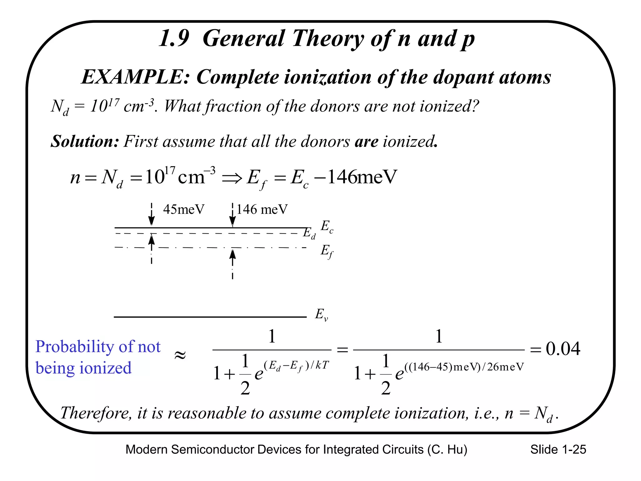
EXAMPLE: Complete ionization of the dopant atoms
Nd = 1017 cm-3. What fraction of the donors are not ionized?
Solution: First assume that all the donors are ionized.
Probability of not
being ionized
04.0
2
1
1
1
2
1
1
1
meV26/)meV)45146((/)(
ee
kTEE fd
Therefore, it is reasonable to assume complete ionization, i.e., n = Nd .
meV146cm10 317
cfd EENn
Ec
Ef
Ev
146 meV
Ed
45meV
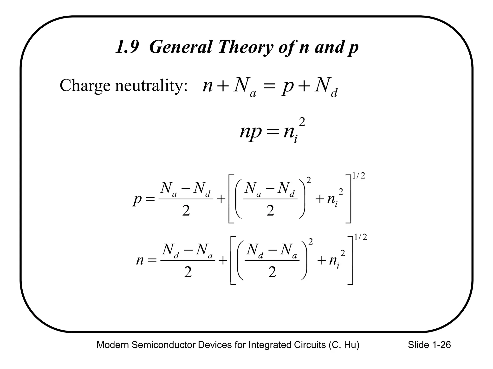
1.9 General Theory of n and p
26.
Modern Semiconductor Devicesfor Integrated Circuits (C. Hu) Slide 1-26
2
innp
da NpNn Charge neutrality:
2/1
2
2
22
i
dada
n
NNNN
p
2/1
2
2
22
i
adad
n
NNNN
n
1.9 General Theory of n and p
27.
Modern Semiconductor Devicesfor Integrated Circuits (C. Hu) Slide 1-27
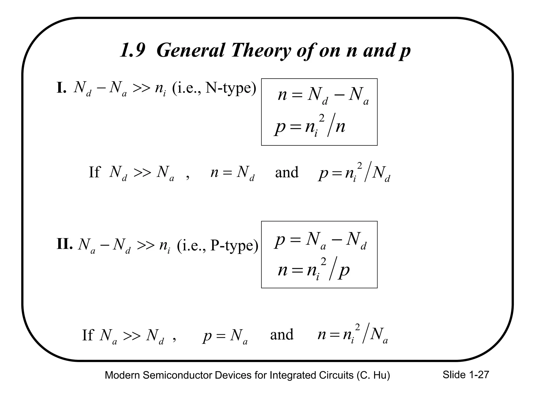
I. (i.e., N-type)
If ,
II. (i.e., P-type)
If ,
ad NNn
nnp i
2
iad nNN
ad NN dNn di Nnp
2
and
ida nNN da NNp
pnn i
2
da NN aNp ai Nnn
2
and
1.9 General Theory of on n and p
28.
Modern Semiconductor Devicesfor Integrated Circuits (C. Hu) Slide 1-28
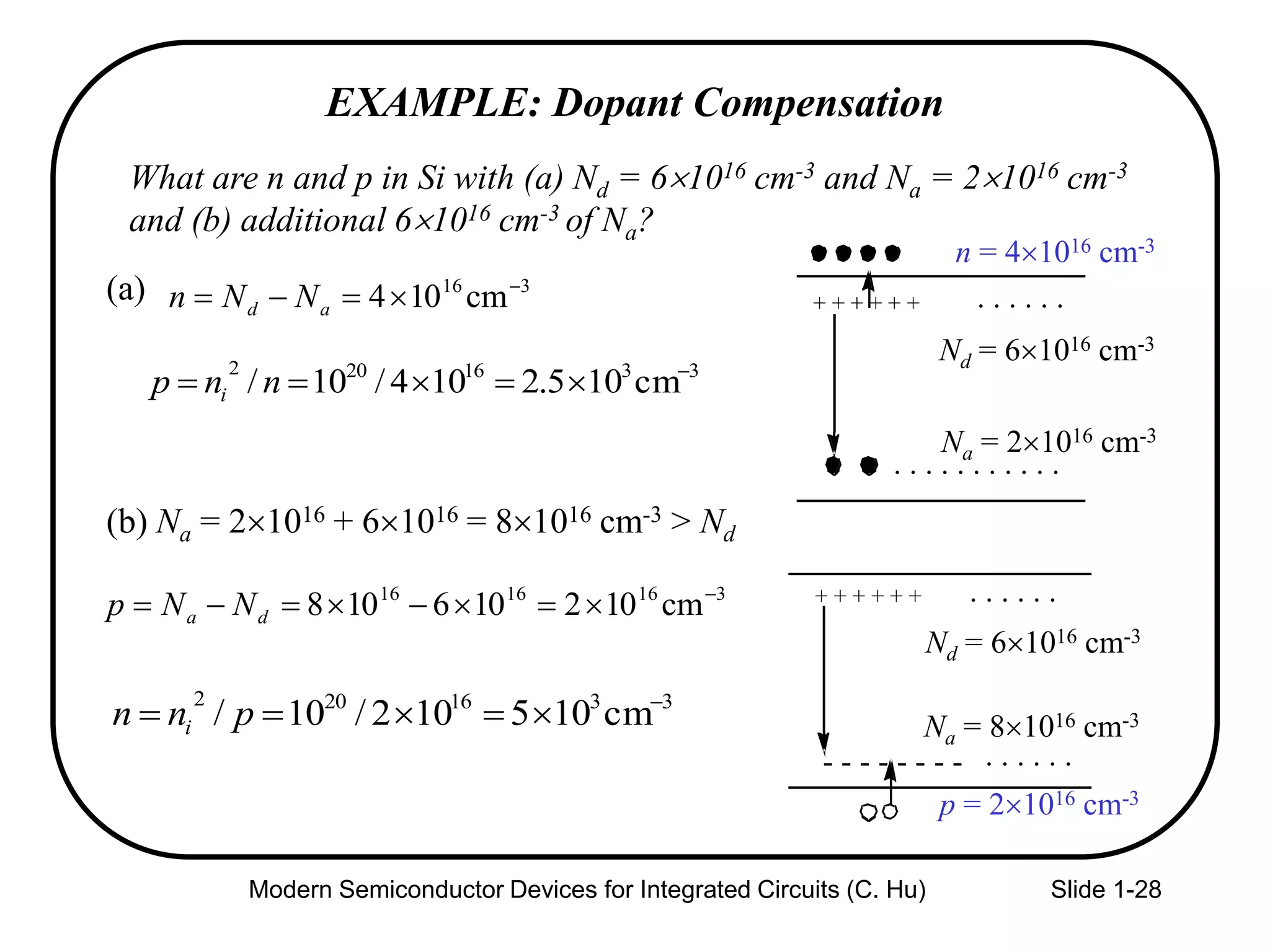
EXAMPLE: Dopant Compensation
What are n and p in Si with (a) Nd = 61016 cm-3 and Na = 21016 cm-3
and (b) additional 61016 cm-3 of Na?
(a)
(b) Na = 21016 + 61016 = 81016 cm-3 > Nd
316
cm104
ad NNn
3316202
cm105.2104/10/
nnp i
3161616
cm102106108
da NNp
3316202
cm105102/10/
pnn i
+ + + + + + . . . . . .
. . . . . . . . . . .
Nd = 61016 cm-3
Na = 21016 cm-3
n = 41016 cm-3
+ + + + + +
- - - - - - - -
. . . . . .
. . . . . .
Nd = 61016 cm-3
Na = 81016 cm-3
p = 21016 cm-3
29.
Modern Semiconductor Devicesfor Integrated Circuits (C. Hu) Slide 1-29
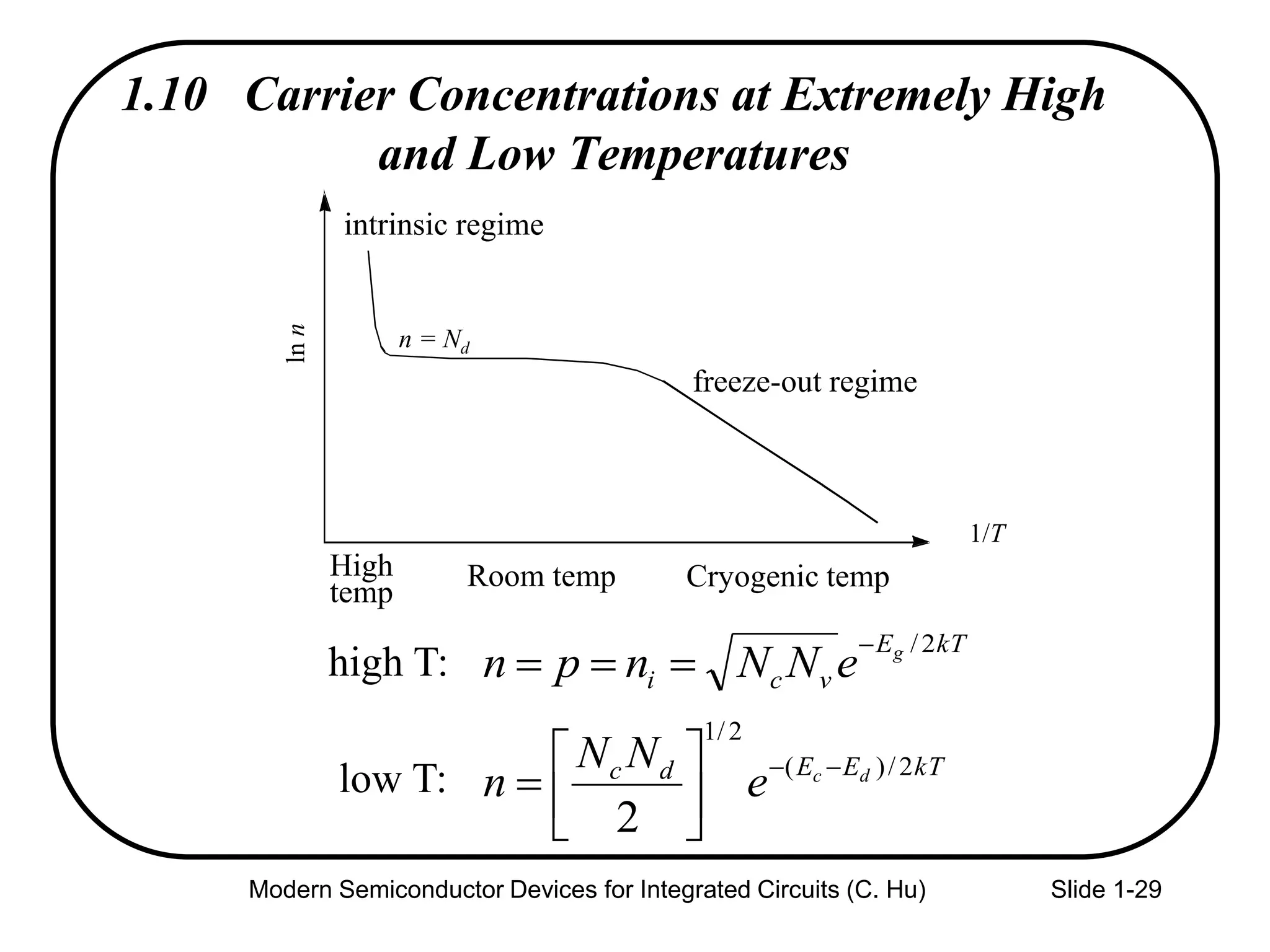
1.10 Carrier Concentrations at Extremely High
and Low Temperatures
intrinsic regime
n = Nd
freeze-out regime
lnn
1/T
High
temp
Room temp Cryogenic temp
kTE
vci
g
eNNnpn
2/
kTEEdc dc
e
NN
n 2/)(
2/1
2
high T:
low T:
30.
Modern Semiconductor Devicesfor Integrated Circuits (C. Hu) Slide 1-30
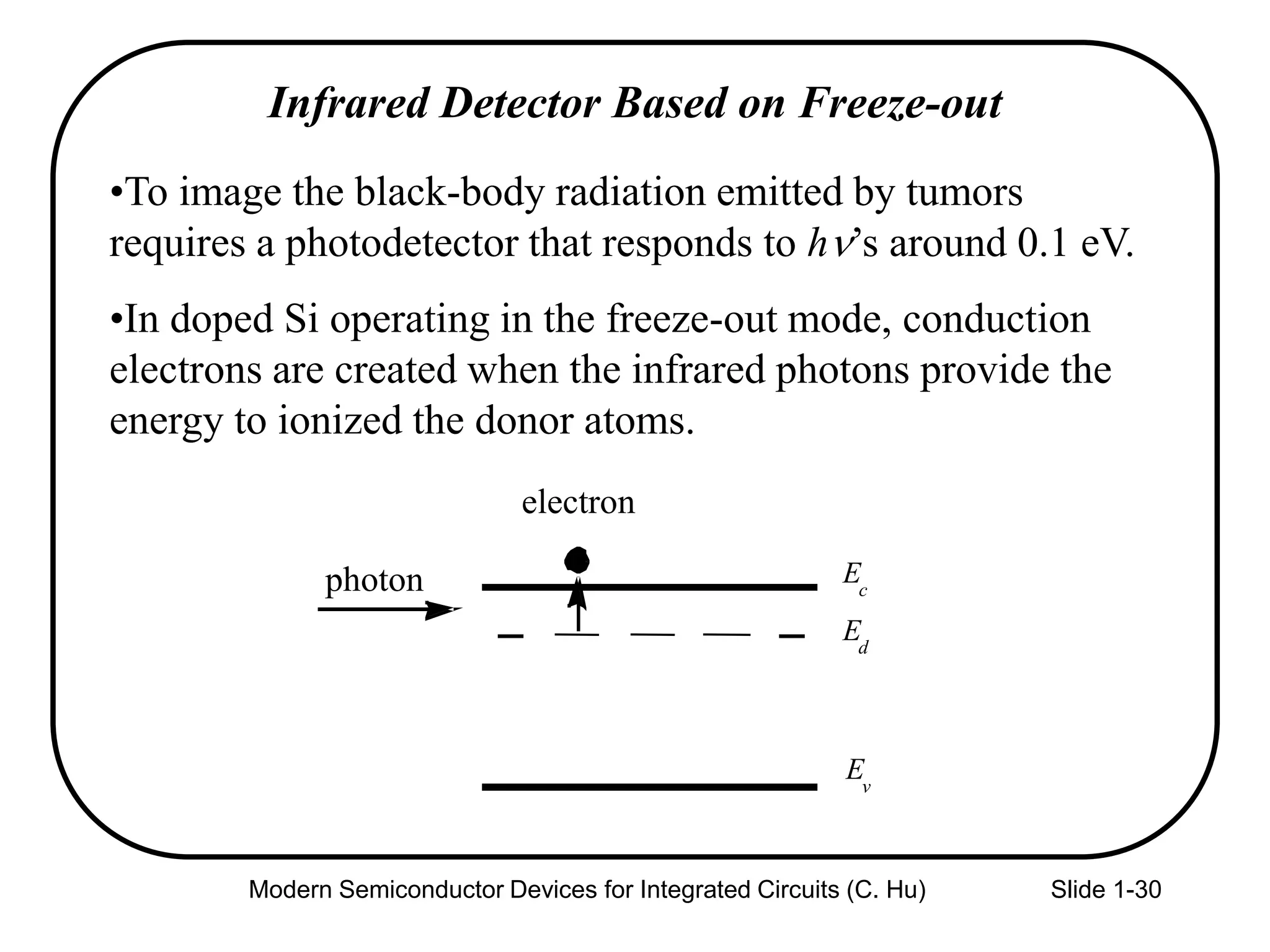
Infrared Detector Based on Freeze-out
•To image the black-body radiation emitted by tumors
requires a photodetector that responds to hn’s around 0.1 eV.
•In doped Si operating in the freeze-out mode, conduction
electrons are created when the infrared photons provide the
energy to ionized the donor atoms.
photon Ec
Ev
electron
Ed
31.
Modern Semiconductor Devicesfor Integrated Circuits (C. Hu) Slide 1-31
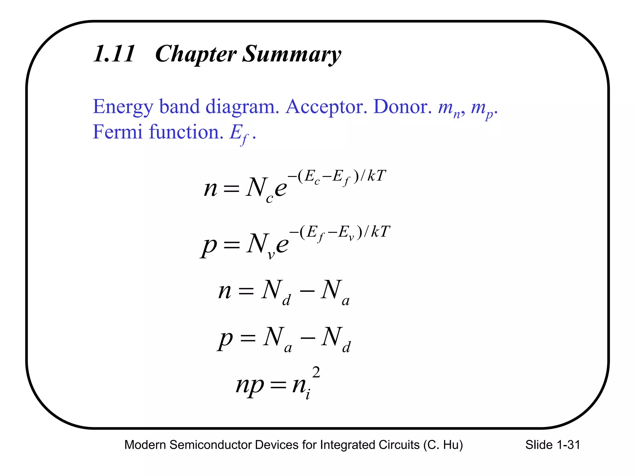
1.11 Chapter Summary
Energy band diagram. Acceptor. Donor. mn, mp.
Fermi function. Ef .
kTEE
c
fc
eNn
/)(
kTEE
v
vf
eNp
/)(
ad NNn
da NNp
2
innp