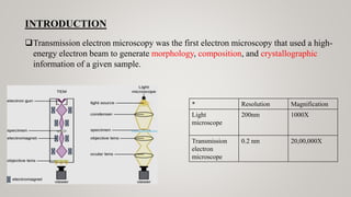
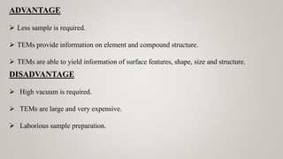
TRANSMISSION ELECTRON
MICROSCOPY (TEM)
AISWARYA GOWRI V S
RESEARCH SCHOLAR
SRMIST KTR
CONTENT
INTRODUCTION
PRINCIPLE
COMPONENTS
WORKING
TRANSMISSION ELECTRON MICROSCOPY VS SCANNING
ELECTRON MICROSCOPY
ADVANTAGE AND DISADVANTAGE OF TRANSMISSION ELECTRON
MICROSCOPY
INTRODUCTION
Transmission electron microscopy was the first electron microscopy that used a high-
energy electron beam to generate morphology, composition, and crystallographic
information of a given sample.
* Resolution Magnification
Light
microscope
200nm 1000X
Transmission
electron
microscope
0.2 nm 20,00,000X
PRINCIPLE
Once the electron beam interacts with the specimen, they are either scattered or are
transmitted based on the mass and density ratio.
The transmitted electron beam will strike the fluorescent screen or a charge-coupled
device (CCD) camera, which will generate an image with varying contrast based on the
intensity of the electron beam.
COMPONENTS
Electron gun: Tungsten and Lanthanum- Hexaboride.
Condenser system: Focus the electron beam to sample.
Image producing system: consists of the objective lens,
aperture lens, and projection lens- (for magnification).
Image recording system: Fluorescent screen, or charge-
coupled device (CCD) camera.
 TEM can operate on two modes, Diffraction mode and image mode
1.Diffraction mode
 The objective lens forms a diffraction pattern in the back focal plane with electrons
scattered and diffracted by the sample and combines them to generate an image in the
image plane.
 Difraction mode can say whether the sample is single crystalline, poly crystalline, or
amorphous by taking Selective Area Diffraction (SAD).
 Single crystal: Produces diffraction pattern consist with a centre spot associated with
transmitted beam and other diffracted spot.
 Poly crystal:Produces diffraction pattern on the rings of different radius.
 Amorphus sample: Follows a halo ring pattern.
single crystall Poly crystall Amorphous
2. Image mode
 Image of the sample is focused and projected onto the screen,
 Which is of two types Darkfield image and Bright field image.
 Bright field images: It is obtained by passing transmitted waves to the objective
aperture.
 Dark field images: It is obtained by allowing the diffracted beam to the objective
aperture.
Bright field image Dark field image
SEM Vs TEM
SEM TEM
 SEM shows only the morphology of samples.
 SEM can resolve objects as close as 20 nm.
 The magnifying power of SEM is up to 50,000X.
 SEM allows for a large amount of sample to be
analyzed at a time.
 Secondary or backscattered electrons arising from the
interaction of electron beam and metal-coated
specimen are collected and the resulting image is
displayed on a computer screen.
 TEM can show many characteristics of the sample,
such as internal composition, morphology, and
crystallization.
 TEM has a much higher resolution than SEM. It can
resolve objects as close as 1 nm i.e. down to near-
atomic levels.
 The magnifying power of TEM is up to 2 million
times.
 With TEM only a small amount of samples can be
analyzed at a time.
 Transmitted electrons hit a fluorescent screen giving
rise to a “shadow image” of the specimen with its
different parts displayed in varied darkness according
to their density. The image can be studied directly by
the operator and photographed with a camera.
ADVANTAGE
 Less sample is required.
 TEMs provide information on element and compound structure.
 TEMs are able to yield information of surface features, shape, size and structure.
DISADVANTAGE
 High vacuum is required.
 TEMs are large and very expensive.
 Laborious sample preparation.
Thank
you……

Transmission electron microscopy-TEM, principle and working.pptx

  • 1.
    TRANSMISSION ELECTRON MICROSCOPY (TEM) AISWARYAGOWRI V S RESEARCH SCHOLAR SRMIST KTR
  • 2.
    CONTENT INTRODUCTION PRINCIPLE COMPONENTS WORKING TRANSMISSION ELECTRON MICROSCOPYVS SCANNING ELECTRON MICROSCOPY ADVANTAGE AND DISADVANTAGE OF TRANSMISSION ELECTRON MICROSCOPY
  • 3.
    INTRODUCTION Transmission electron microscopywas the first electron microscopy that used a high- energy electron beam to generate morphology, composition, and crystallographic information of a given sample. * Resolution Magnification Light microscope 200nm 1000X Transmission electron microscope 0.2 nm 20,00,000X
  • 4.
    PRINCIPLE Once the electronbeam interacts with the specimen, they are either scattered or are transmitted based on the mass and density ratio. The transmitted electron beam will strike the fluorescent screen or a charge-coupled device (CCD) camera, which will generate an image with varying contrast based on the intensity of the electron beam.
  • 5.
    COMPONENTS Electron gun: Tungstenand Lanthanum- Hexaboride. Condenser system: Focus the electron beam to sample. Image producing system: consists of the objective lens, aperture lens, and projection lens- (for magnification). Image recording system: Fluorescent screen, or charge- coupled device (CCD) camera.
  • 6.
     TEM canoperate on two modes, Diffraction mode and image mode 1.Diffraction mode  The objective lens forms a diffraction pattern in the back focal plane with electrons scattered and diffracted by the sample and combines them to generate an image in the image plane.  Difraction mode can say whether the sample is single crystalline, poly crystalline, or amorphous by taking Selective Area Diffraction (SAD).  Single crystal: Produces diffraction pattern consist with a centre spot associated with transmitted beam and other diffracted spot.  Poly crystal:Produces diffraction pattern on the rings of different radius.  Amorphus sample: Follows a halo ring pattern. single crystall Poly crystall Amorphous
  • 7.
    2. Image mode Image of the sample is focused and projected onto the screen,  Which is of two types Darkfield image and Bright field image.  Bright field images: It is obtained by passing transmitted waves to the objective aperture.  Dark field images: It is obtained by allowing the diffracted beam to the objective aperture. Bright field image Dark field image
  • 8.
    SEM Vs TEM SEMTEM  SEM shows only the morphology of samples.  SEM can resolve objects as close as 20 nm.  The magnifying power of SEM is up to 50,000X.  SEM allows for a large amount of sample to be analyzed at a time.  Secondary or backscattered electrons arising from the interaction of electron beam and metal-coated specimen are collected and the resulting image is displayed on a computer screen.  TEM can show many characteristics of the sample, such as internal composition, morphology, and crystallization.  TEM has a much higher resolution than SEM. It can resolve objects as close as 1 nm i.e. down to near- atomic levels.  The magnifying power of TEM is up to 2 million times.  With TEM only a small amount of samples can be analyzed at a time.  Transmitted electrons hit a fluorescent screen giving rise to a “shadow image” of the specimen with its different parts displayed in varied darkness according to their density. The image can be studied directly by the operator and photographed with a camera.
  • 10.
    ADVANTAGE  Less sampleis required.  TEMs provide information on element and compound structure.  TEMs are able to yield information of surface features, shape, size and structure. DISADVANTAGE  High vacuum is required.  TEMs are large and very expensive.  Laborious sample preparation.
  • 11.