Downloaded 34 times
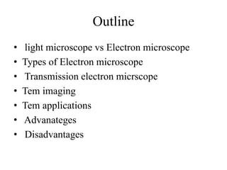
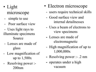
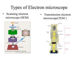
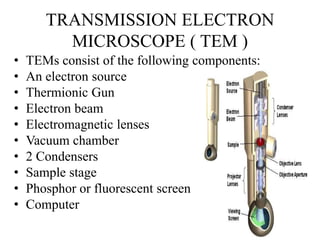
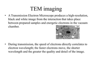
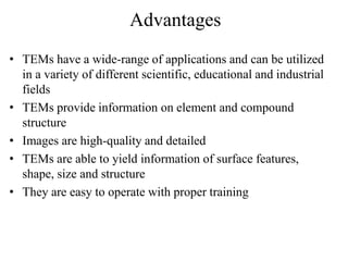
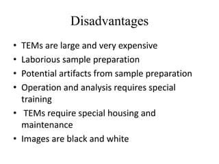


This document discusses the transmission electron microscope (TEM). It begins by comparing light microscopes and electron microscopes. It then describes the key components of a TEM, including the electron source, lenses, vacuum chamber, and screen. It explains that TEMs produce high-resolution black and white images through the interaction of electrons with prepared samples. Applications of TEM include studying crystals, metals, and semiconductor analysis. Advantages are high-quality images and structure information, while disadvantages include large size, expense, specialized training and sample preparation.


