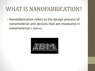
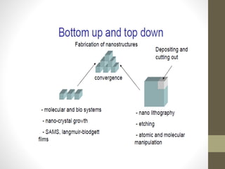
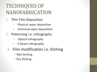
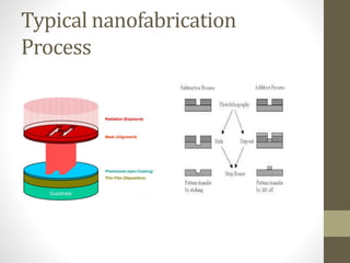
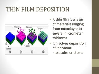
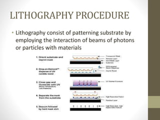
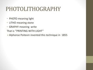
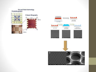
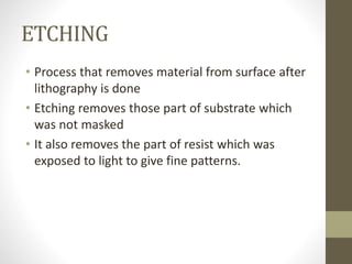
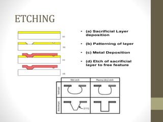
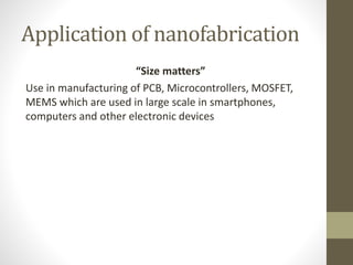
The document discusses nanofabrication techniques used to design nanomaterials and devices measured in nanometers. It describes common nanofabrication processes like thin film deposition using physical vapor deposition or chemical vapor deposition, patterning using optical or e-beam lithography, and etching using wet or dry methods. Typical applications of nanofabrication include manufacturing printed circuit boards, microcontrollers, and MEMS devices used in smartphones and computers.