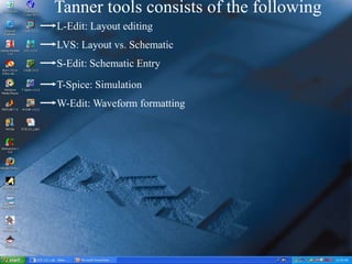
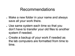
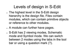
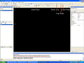
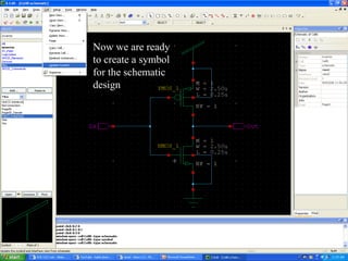
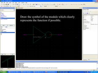
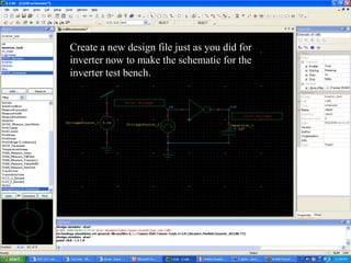
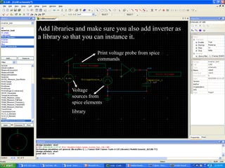
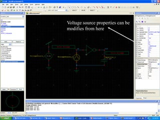
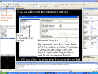
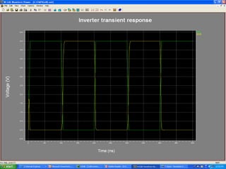
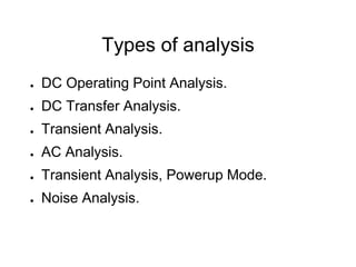
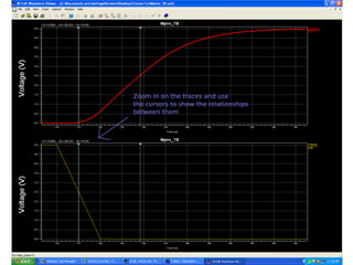
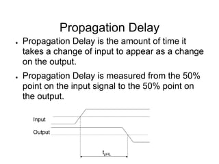
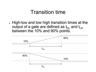
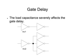
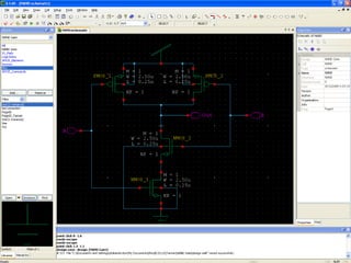
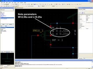
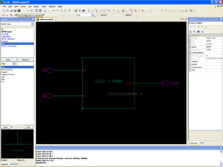
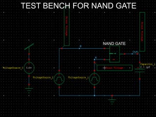
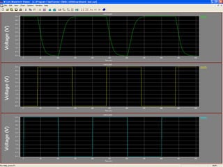
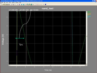
ECE122 – Digital Electronics & Design
Tanner Tools Tutorial
Ritu Bajpai
Objective of the lab
● To develop an understanding of design and
simulation of digital logic circuits.
● To get a basic understanding of layout of
electronic circuits.
● We will use Tanner tools for design and
simulation.
● This lab introduces us to Tanner tools.
Introduction to Tanner tools
● Tanner tool- simulation tool for the class
● Upgraded from last year
● Some slides may look different as you will
see on your computer
● Slides will be updated to correspond with the
new version of Tanner as we advance into
the semester
Tanner tools consists of the following
L-Edit: Layout editing
LVS: Layout vs. Schematic
S-Edit: Schematic Entry
T-Spice: Simulation
W-Edit: Waveform formatting
This is S-Edit
For creating new design go
File->New->New design
Enter design name and the folder name where you
want to save your work.
Recommendations
● Make a new folder in your name and always
save all your work there.
● Use same system each time so that you
don’t have to transfer your old files to another
system if needed.
● Create a backup of your work if needed as
the lab computers are formatted from time to
time.
Now go to Cell->New View
Hit OK to start with new cell schematic design
Levels of design in S-Edit
● The highest level in the S-Edit design
hierarchy is the design file. Files contain
modules, which can contain primitive objects
or reference to other modules.
● A module can further have pages.
● S-Edit has 2 viewing modes, Schematic
mode and Symbol mode. We can switch
between 2 modes using the tabs in the tool
bar or using a question mark (?).
Select tool Draw wire
Cap Node
Label Node
For more help with S-Edit go to
Help->Tutorial
Library file path
C:DesktopStudentMy DocumentsTanner
EDATanner Tools
v15.0ProcessGeneric_250nmGeneric_250nm.tanner
Click here to
add libraries
Browse the library file from the path above and hit OK.
There are other libraries in the process folder. Feel free to add
them and see what components they have. For example we
will add spice_components and spice_commands from the
library “standard_library”.
Now we will instance first element
NMOS from the library Devices and hit
done.
Some useful tips
● To move an object: Use center wheel of the
mouse.
● For zoom in and zoom out use + and –
respectively from the key board.
● To view/edit object properties, select object
and use CTRL+E.
● Do not use space in your design names.
● Do not use special characters in port names.
Introduction to MOSFET
● A MOSFET can be
• PMOS
• NMOS
● A MOSFET is a four terminal device. Four
terminals are:
• Gate
• Drain
• Source
• Bulk
● A MOSFET is symmetrical device unlike a
BJT which means either terminal can be
drain or source unless connected in a circuit.
Introduction to MOSFET
● For a PMOS source is always connected to
highest voltage in the circuit.
● For an NMOS source is always connected to
lowest voltage in a circuit.
● The bulk is always shorted to the source for
both devices.
Introduction to MOSFET
● The bulk terminal is identified by an arrow.
● We can distinguish PMOS symbol from
NMOS symbol as follows:
• PMOS bulk has arrow coming out .
• NMOS bulk has arrow going in. (Tip: remember
‘in’ sounds like N.)
• PMOS gate has a bubble attached to it.
● There can be different symbols for PMOS
and NMOS for example the bulk may not be
shown but the above points hold good for the
MOSFETS we will be using from SCMOS
library in S-Edit.
Schematic design of an inverter
● Today we will design an inverter schematic in
S-Edit.
● In this class we will design CMOS based
logic circuits.
● Thus an inverter consists of a PMOS and an
NMOS connected in series with PMOS
source connected to Vdd and NMOS source
connected to Gnd.
● Input is applied at the gates.
● Output is collected from the drains which are
connected together.
Vdd from library Misc
Gnd from library Misc
PMOS from library
Devices
Input port
Output port
Now we are ready
to create a symbol
for the schematic
design
Draw the symbol of the module which clearly
represents the function if possible.
Create a new design file just as you did for
inverter now to make the schematic for the
inverter test bench.
Add libraries and make sure you also add inverter as
a library so that you can instance it.
Voltage
sources from
spice elements
library
Print voltage probe from spice
commands
Voltage source properties can be
modifies from here
Now we will set up the simulation settings
Click to pop
up the set up
window
Browse the library file
My DocumentsTanner EDATanner Tools
v15.0ProcessGeneric_250nm_TechGeneri
c_250nm.lib. Add a space followed by
letters TT at the end of the path. This is
must for spice to recognize this path.
Select
Transient/Fourier
analysis
Hit OK and click the green play button on the top left
Types of analysis
● DC Operating Point Analysis.
● DC Transfer Analysis.
● Transient Analysis.
● AC Analysis.
● Transient Analysis, Powerup Mode.
● Noise Analysis.
Types of analysis
● DC operating point analysis: It finds the
circuit’s steady-state condition, obtained (in
principle) after the input voltages have been
applied for an infinite amount of time.
● DC Transfer Analysis: It is used to study the
voltage or current at one set of points in a
circuit as a function of the voltage or current
at another set of points. This is done by
sweeping the source variables over specified
ranges, and recording the output.
Types of Analysis
● Transient Analysis: It provides information on
how circuit elements vary with time.
● AC Analysis: It characterizes the circuit’s
behavior dependence on small signal input
frequency.
● Transient Analysis power up mode: Some
circuits do not have a DC steady state so it is
difficult to specify there initial state. This is
done using power up option of the .tran
command. It sets entire circuit to zero for
time equal to 0.
Propagation Delay
● Propagation Delay is the amount of time it
takes a change of input to appear as a change
on the output.
● Propagation Delay is measured from the 50%
point on the input signal to the 50% point on
the output.
Input
Output
tpHL
Transition time
● High-low and low high transition times at the
output of a gate are defined as tHL and tLH
between the 10% and 90% points.
tLH
10%
90%
tHL
10%
90%
Gate Delay
● The load capacitance severely affects the
gate delay.
Inv1
Inv2
Simulating NAND gate
● Next we will make a NAND gate using p and
n MOSFET and test its performance.
Note parameters
W=2.50u and L=0.25u
NAND GATE
TEST BENCH FOR THE NAND GATE
NAND GATE
TEST BENCH FOR NAND GATE
NAND GATE
TEST BENCH FOR NAND GATE
tpHL
Record the propagation delay
● Record tpHL and tpLH for the NAND gate.
● Record the waveform for the same.
Lab Reports
● Strictly adhere to the lab report format and
other instructions on the website
● No late submissions without prior permission

Tanner tools

  • 1.
    ECE122 – DigitalElectronics & Design Tanner Tools Tutorial Ritu Bajpai
  • 2.
    Objective of thelab ● To develop an understanding of design and simulation of digital logic circuits. ● To get a basic understanding of layout of electronic circuits. ● We will use Tanner tools for design and simulation. ● This lab introduces us to Tanner tools.
  • 3.
    Introduction to Tannertools ● Tanner tool- simulation tool for the class ● Upgraded from last year ● Some slides may look different as you will see on your computer ● Slides will be updated to correspond with the new version of Tanner as we advance into the semester
  • 4.
    Tanner tools consistsof the following L-Edit: Layout editing LVS: Layout vs. Schematic S-Edit: Schematic Entry T-Spice: Simulation W-Edit: Waveform formatting
  • 5.
  • 6.
    For creating newdesign go File->New->New design
  • 7.
    Enter design nameand the folder name where you want to save your work.
  • 8.
    Recommendations ● Make anew folder in your name and always save all your work there. ● Use same system each time so that you don’t have to transfer your old files to another system if needed. ● Create a backup of your work if needed as the lab computers are formatted from time to time.
  • 9.
    Now go toCell->New View
  • 10.
    Hit OK tostart with new cell schematic design
  • 11.
    Levels of designin S-Edit ● The highest level in the S-Edit design hierarchy is the design file. Files contain modules, which can contain primitive objects or reference to other modules. ● A module can further have pages. ● S-Edit has 2 viewing modes, Schematic mode and Symbol mode. We can switch between 2 modes using the tabs in the tool bar or using a question mark (?).
  • 12.
    Select tool Drawwire Cap Node Label Node
  • 13.
    For more helpwith S-Edit go to Help->Tutorial
  • 14.
    Library file path C:DesktopStudentMyDocumentsTanner EDATanner Tools v15.0ProcessGeneric_250nmGeneric_250nm.tanner Click here to add libraries Browse the library file from the path above and hit OK. There are other libraries in the process folder. Feel free to add them and see what components they have. For example we will add spice_components and spice_commands from the library “standard_library”.
  • 15.
    Now we willinstance first element NMOS from the library Devices and hit done.
  • 16.
    Some useful tips ●To move an object: Use center wheel of the mouse. ● For zoom in and zoom out use + and – respectively from the key board. ● To view/edit object properties, select object and use CTRL+E. ● Do not use space in your design names. ● Do not use special characters in port names.
  • 17.
    Introduction to MOSFET ●A MOSFET can be • PMOS • NMOS ● A MOSFET is a four terminal device. Four terminals are: • Gate • Drain • Source • Bulk ● A MOSFET is symmetrical device unlike a BJT which means either terminal can be drain or source unless connected in a circuit.
  • 18.
    Introduction to MOSFET ●For a PMOS source is always connected to highest voltage in the circuit. ● For an NMOS source is always connected to lowest voltage in a circuit. ● The bulk is always shorted to the source for both devices.
  • 19.
    Introduction to MOSFET ●The bulk terminal is identified by an arrow. ● We can distinguish PMOS symbol from NMOS symbol as follows: • PMOS bulk has arrow coming out . • NMOS bulk has arrow going in. (Tip: remember ‘in’ sounds like N.) • PMOS gate has a bubble attached to it. ● There can be different symbols for PMOS and NMOS for example the bulk may not be shown but the above points hold good for the MOSFETS we will be using from SCMOS library in S-Edit.
  • 20.
    Schematic design ofan inverter ● Today we will design an inverter schematic in S-Edit. ● In this class we will design CMOS based logic circuits. ● Thus an inverter consists of a PMOS and an NMOS connected in series with PMOS source connected to Vdd and NMOS source connected to Gnd. ● Input is applied at the gates. ● Output is collected from the drains which are connected together.
  • 21.
    Vdd from libraryMisc Gnd from library Misc PMOS from library Devices Input port Output port
  • 22.
    Now we areready to create a symbol for the schematic design
  • 23.
    Draw the symbolof the module which clearly represents the function if possible.
  • 24.
    Create a newdesign file just as you did for inverter now to make the schematic for the inverter test bench.
  • 25.
    Add libraries andmake sure you also add inverter as a library so that you can instance it. Voltage sources from spice elements library Print voltage probe from spice commands
  • 26.
    Voltage source propertiescan be modifies from here
  • 27.
    Now we willset up the simulation settings Click to pop up the set up window Browse the library file My DocumentsTanner EDATanner Tools v15.0ProcessGeneric_250nm_TechGeneri c_250nm.lib. Add a space followed by letters TT at the end of the path. This is must for spice to recognize this path. Select Transient/Fourier analysis Hit OK and click the green play button on the top left
  • 29.
    Types of analysis ●DC Operating Point Analysis. ● DC Transfer Analysis. ● Transient Analysis. ● AC Analysis. ● Transient Analysis, Powerup Mode. ● Noise Analysis.
  • 30.
    Types of analysis ●DC operating point analysis: It finds the circuit’s steady-state condition, obtained (in principle) after the input voltages have been applied for an infinite amount of time. ● DC Transfer Analysis: It is used to study the voltage or current at one set of points in a circuit as a function of the voltage or current at another set of points. This is done by sweeping the source variables over specified ranges, and recording the output.
  • 31.
    Types of Analysis ●Transient Analysis: It provides information on how circuit elements vary with time. ● AC Analysis: It characterizes the circuit’s behavior dependence on small signal input frequency. ● Transient Analysis power up mode: Some circuits do not have a DC steady state so it is difficult to specify there initial state. This is done using power up option of the .tran command. It sets entire circuit to zero for time equal to 0.
  • 33.
    Propagation Delay ● PropagationDelay is the amount of time it takes a change of input to appear as a change on the output. ● Propagation Delay is measured from the 50% point on the input signal to the 50% point on the output. Input Output tpHL
  • 34.
    Transition time ● High-lowand low high transition times at the output of a gate are defined as tHL and tLH between the 10% and 90% points. tLH 10% 90% tHL 10% 90%
  • 35.
    Gate Delay ● Theload capacitance severely affects the gate delay. Inv1 Inv2
  • 36.
    Simulating NAND gate ●Next we will make a NAND gate using p and n MOSFET and test its performance.
  • 38.
  • 40.
    NAND GATE TEST BENCHFOR THE NAND GATE NAND GATE TEST BENCH FOR NAND GATE NAND GATE TEST BENCH FOR NAND GATE
  • 42.
  • 43.
    Record the propagationdelay ● Record tpHL and tpLH for the NAND gate. ● Record the waveform for the same.
  • 44.
    Lab Reports ● Strictlyadhere to the lab report format and other instructions on the website ● No late submissions without prior permission