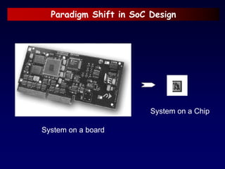
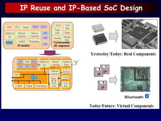
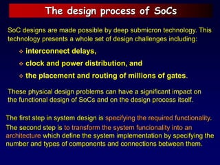
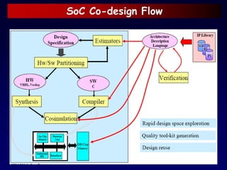
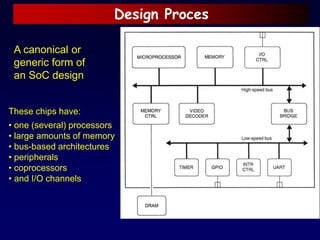
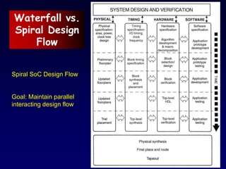
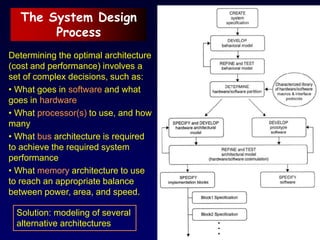
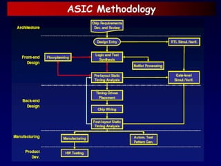
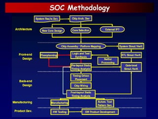
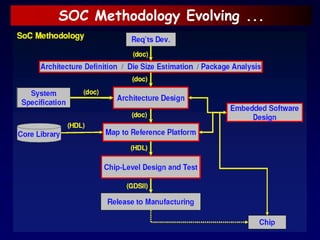
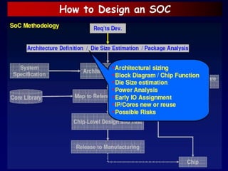
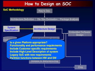
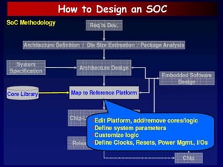
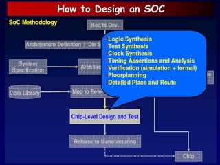
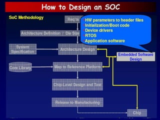
System on Chip (SoC)
Design
Outline
• Key Trends and The SoC Paradigm
• System on Chip
Architecture
Design
Cores
Interconnection
• Cost Benefits of SoC
• Examples
• Conclusion
Moore’s Law and Technology Scaling
…the performance of an IC, including the number components on it, doubles
every 18-24 months with the same chip price ... - Gordon Moore - 1960
The Productivity Gap
􀂈 100M logic gates in 90nm = Logic of 1000 ARM7’s
􀂈 Current 0.13u SoC’s: 10M$ ~100M$ design cost
ITRS Roadmap
H.P. – high performance microprocessor, μP – microprocessors
H.H. – hand-hold products, SoC – system-on-chip
Silicon technology roadmap
low power SoC
high performance
MPU/SoC
2001 2004 2010 2001 2004 2010
gate length (nm) 130 90 45 90 53 25
supply voltage 1.2 1 0.6 1.1 1 0.6
transistor count (M) 3.3 8.3 40 276 553 2212
chip size (mm2) 100 120 144 310 310 310
clock frequency (GHz) 0.15 0.3 0.6 1.7 2.4 4.7
wiring levels 6 7 9 7 8 10
max power (W) 0.1 0.1 0.1 130 160 218
• intrinsic capability of ICs (transistor count / gate delay)
grows with ~ 50% per year (Moore’s Law)
• power limits the performance
Introduction - History
• First generation chips contained a few transistors.
• Today, silicon technology allows us to build chips consisting of
hundreds of millions of transistors (Intel Pentium IV: 0.09
micron). This technology has enabled new levels of system
integration onto a single chip.
• Mobile phones, portable computers and Internet appliances will
be built using a single chip.
• The demand for more powerful products and the huge capacity
of today’ s silicon technology have moved System-on-Chip (SoC)
designs from leading edge to mainstream design practice.
• “System on Chip” (SoC) technology will put the maximum
amount of technology into the smallest possible space.
Electronic systems
Systems on chip are everywhere
Technology advances enable increasingly more complex designs
Central Question: how to exploit deep-
submicron technologies efficiently?
Main Challenges of Wireless Sensor Network
 Energy dissipation
Reduce radiated power
More power efficient radio
Energy efficient protocols and routing algorithms
Better trade-off between communication and local computing
 Size
Higher integration (System-on-Chip or SoC)
 Cost
Standard Digital CMOS Technology
Evolution of Microelectronics: the SoC Paradigm
Silicon Process Technology
•􀂈 0.13μm CMOS
•􀂈 ~100 millions of devices, 3 GHz internal Clock
Paradigm Shift in SoC Design
System on a board
System on a Chip
Evolutionary Problems
􀂈 Key Challenges
– Improve productivity
– HW/SW codesign
– Integration of analog & RF IPs
– Improved DFT
Emerging new technologies:
– Greater complexity
– Increased performance
– Higher density
– Lower power dissipation
􀂈 Evolutionary techniques:
- IP (Intellectual Property) based design
- Platform-based design
Migration from ASICs to SoCs
ASICs are logic chips designed by end customers to
perform a specific function for a desired application.
ASIC vendors supply libraries for each technology
they provide. In most cases, these libraries contain
predesigned and preverified logic circuits.
ASIC technologies are:
 gate array
 standard cell
 full custom
Migration from ASICs to SoCs
In the mid-1990s, ASIC technology evolved from a
chip-set philosophy to an embedded-cores-based
system-on-a-chip concept.
An SoC is an IC designed by stitching
together multiple stand-alone VLSI
designs to provide full functionality for
an application.
An SoC compose of predesigned
models of complex functions known
as cores (terms such as intellectual
property block, virtual components,
and macros) that serve a variety of
applications.
Three forms of SoC design
The scenario for SoC design is characterized by three forms:
1. ASIC vendor design: This refers to the design in which all the
components in the chip are designed as well as fabricated by
an ASIC vendor.
2. Integrated design: This refers to the design by an ASIC vendor
in which all components are not designed by that vendor. It
implies the use of cores obtained from some other source
such as a core/IP vendor or a foundry.
3. Desktop design: This refers to the design by a fabless
company that uses cores which for the most part have been
obtained from other source such as IP companies, EDA
companies, design services companies, or a foundry.
SoC Design Challenges
Why does it take longer to design SOCs compared to
traditional ASICs?
We must examine factors influencing the degree of difficulty and
Turn Around Time (TAT) (the time taken from gate-level netlist to
metal mask-ready stage) for designing ASICs and SOCs.
For an ASIC, the following factors influence TAT:
• Frequency of the design
• Number of clock domains
• Number of gates
• Density
• Number of blocks and sub-blocks
The key factor that influences TAT for SOCs is system
integration (integrating different silicon IPs on the same IC).
SoC Design Challenges
Levarage Internal Bandwidth vs External Bandwidth
SoCs vs. ASICs
 SoC methodology is an incremental step over ASIC
methodology
 SoC design is significantly more complex
 Need cross-domain optimizations
 IP reuse and Platform-based design increase
productivity, but not enough
 Even with extensive IP reuse, many of the ASICs
design problems remain, plus many more ...
 Productivity increase far from closing design gap
 SoC is not just a large ASIC
 Architectural approach involving significant design reuse
 Addresses the cost and time-to-market problems
From ASICs to SoCs
Technology vs. Productivity vs. Complexity
System on Chip benefits
CPU
DSP
Ip-
Sec
mem
X
USB
hub
mem
CPU DSP USB
hub
Ip-
Sec
X
Proc
Co-
Proc
IP cores
Typical : $10
Up to now : collection of chips
Now : collection of cores
Typical : $70
Typical approach :
Define requirements
Design with off-the shelf chips
- at 0.5 year mark : first prototypes
- 1 year : ship with low margins/loss
start ASIC integration
- 2 years : ASIC-based prototypes
- 2.5 years : ship, make profits (with
competition)
With SoC
Define requirements
Design with off-the shelf cores
- at 0.5 year mark : first prototypes
- 1 year : ship with high margin and
market share
Typical applications of SoC
An SoC is a system on an IC that integrates software and hardware
Intellectual Property (IP) using more than one design methodology for the
purpose of defining the funcionality and behavior of the proposed system.
The designed system
is application specific.
Typical applications of SoC:
 consumer devicecs,
 networking,
 communications, and
 other segments of the electronics industry.
microprocessor, media processor,
GPS controllers, cellular phones,
GSM phones, smart pager ASICs,
digital television, video games,
PC-on-a-chip
A common set of problems facing everyone who is
designing complex chips
• Time-to-market pressures demand rapid development.
• Quality of results (performance, area, power) - key to market success.
• Increasing chip complexity makes verification more difficult.
• Deep submicron issues make timing closure more difficult.
• The development team has different levels and areas of expertise, and
is often scattered throughout the world.
• Design team members may have worked on similar designs in the past,
but cannot reuse these designs because the design flow, tools, and
guidelines have changed.
• SoC designs include embedded processor cores, and thus a significant
software component, which leads to additional methodology, process,
and organizational challenges.
Reusing macros (called “cores”, or IP) that have already been
designed and verified helps to address all of the problems above.
Design for Reuse
To overcome the design gap, design reuse - the use of pre-
designed and pre-verified cores, or reuse of the existing designs
becomes a vital concept in design methodology.
An effective block-based design methodology requires an
extensive library of reusable blocks, or macros, and it is based
on the following principles:
 The macro must be extremely easy to integrate into the
overall chip design.
 The macro must be so robust that the integrator has to
perform essentially no functional verification of internals of the
macro.
The challenge for designers is not whether to
adopt reuse, but how to employ it effectively.
Design for Reuse
To be fully reusable, the hardware macro must be:
• Designed to solve a general problem – easily configurable to fit
different applications.
• Designed for use in multiple technologies – For soft macros, this
mean that the synthesis scripts must produce satisfactory quality of results with a
variety of libraries. For hard macros, this means having an effective porting strategy
for mapping the macro onto new technologies.
• Designed for simulation with a variety of simulators – Good
design reuse practices dictate that both a Verilog and VHDL version of each model
and verification testbench should be available, and they should work with all the
major commercial simulators.
• Designed with standards-based interfaces – Unique or custom
interfaces should be used only if no standards-based interface exists.
Design for Reuse – cont.
To be fully reusable, the hardware macro must be:
• Verified independently of the chip in which it will be used –
Often, macros are designed and only partially tested before being integrated into
a chip for verification. Reusable designs must have full, stand-alone testbenches
and verification suites that afford very high levels of test coverage.
• Verified to a high level of confidence – This usually means very
rigorous verification as well as building a physical prototype that is tested in an
actual system running real software.
• Fully documented in terms of appropriate applications and
restrictions – In particular, valid configurations and parameter values must be
documented. Any restrictions on configurations or parameter values must be
clearly stated. Interfacing requirements and restrictions on how the macro can be
used must be documented.
Intellectual Property
Utilizing the predesigned modules
enables:
 to avoid reinventing the wheel for
every new product,
 to accelerate the development of
new products,
 to assemble various blocks of a
large ASIC/SoC quite rapidly,
 to reduce the possibility of failure
based on design and verification of
a block for the first time.
These predesigned modules are commonly called
Intellectual Property (IP) cores or Virtual Components (VC).
Resources vs. Number of Uses
$, Time
Multiple Uses
With Design Reuse
Without Design Reuse
Intellectual Property Categories
IP cores are classified into three distinct categories:
Hard IP cores consist of hard layouts using particular physical design
libraries and are deliverid in masked-level designed blocks (GDSII
format). The integration of hard IP cores is quite simple, but hard cores
are technology dependent and provide minimum flexibility and portability
in reconfiguration and integration.
Soft IP cores are delivered as RTL VHDL/Verilog code to provide
functional descriptions of IPs. These cores offer maximum flexibility and
reconfigurability to match the requirements of a specific design
application, but they must be synthesized, optimized, and verified by their
user before integration into designs.
Firm IP cores bring the best of both worlds and balance the high
performance and optimization properties of hard IPs with the flexibility of
soft IPs.These cores are delivered in form of targeted netlists to specific
physical libraries after going through synthesis without performing the
physical layout.
Trade-offs among soft, firm, and hard cores
Resusability
portability
flexibility
Predictability, performance, time to market
Soft
core
Firm
core
Hard
core
Comparison of Different IP Formats
IP Format Representation Optimization Technology Reusability
Hard GDSII Very High Technology
Dependent
Low
Soft RTL Low Technology
Independent
Very High
Firm Target Netlist High Technology
Generic
High
Examples of IPs
IP Reuse and IP-Based SoC Design
What is MPSoC
MPSoC is a system-on-chip that contains multiple
instruction-set processors (CPUs).
The typical MPSoC is a heterogeneous multiprocessor:
there may be several different types of processing elements (PEs),
the memory system may be heterogeneously distributed around
the machine, and the interconnection network between the PEs
and the memory may also be heterogeneous.
MPSoCs often require large amounts of memory. The device may
have embedded memory on-chip as well as relying on off-chip
commodity memory.
The design process of SoCs
SoC designs are made possible by deep submicron technology. This
technology presents a whole set of design challenges including:
 interconnect delays,
 clock and power distribution, and
 the placement and routing of millions of gates.
These physical design problems can have a significant impact on
the functional design of SoCs and on the design process itself.
The first step in system design is specifying the required functionality.
The second step is to transform the system funcionality into an
architecture which define the system implementation by specifying the
number and types of components and connections between them.
Define Hardware-Software Codesign
Hardware-Software Codesign is the concurrent and co-operative
design of hardware and software components of a system.
The SoC design process is a hardware-software codesign in
which design productivity is achived by design reuse.
The design process is the set of design tasks that transform
an abstract specification model into an architectural model.
SoC Co-design Flow
Design Proces
A canonical or
generic form of
an SoC design
These chips have:
• one (several) processors
• large amounts of memory
• bus-based architectures
• peripherals
• coprocessors
• and I/O channels
Waterfall vs.
Spiral Design Flow
The traditional model for
ASIC development is often
called a waterfall model.
The project transitions
from phase to phase in a
step function, never
returning to the activities
of the previous phase.
Waterfall vs. Spiral Design Flow
As complexity increases, geometry shrinks, and time-to-market
pressures continue to escalate, chip designers are moving from
the old waterfall model to the newer spiral development model.
In the spiral model, the design team works on multiple aspects of
the design simultaneously, incrementally improving in each area
as the design converges on completion.
The spiral SoC design flow is characterized by:
 Parallel, concurrent development of hardware and software
 Parallel verification and synthesis of modules
 Floorplanning and place-and-route included in the synthesis
process
 Modules developed only if a pre-designed hard or soft macro
is not available
 Planned iteration throughout
Waterfall vs.
Spiral Design
Flow
Spiral SoC Design Flow
Goal: Maintain parallel
interacting design flow
Top-Down vs. Bottom-Up
The classic top-down design process can be viewed as a recursive routine
that begins with specification and decomposition, and ends with integration
and verification:
 Write complete specifications for the system or subsystem being designed.
 Refine its architecture and algorithms, including software design and
hardware/software cosimulation if necessary.
 Decompose the architecture into well-defined macros.
 Design or select macros; this is where the recursion occurs.
 Integrate macros into the top level; verify functionality and timing.
 Deliver the subsystem/system to the next higher level of integration; at the
top level, this is tapeout.
 Verify all aspects of the design (functionality, timing, etc.).
Top-Down vs. Bottom-Up
A top-down methodology assumes that the lowest level
blocks specified can, in fact, be designed and built. If it turns
out that a block is not feasible to design, the whole
specification process has to be repeated.
For this reason, real world design teams usually use a
mixture of top-down and bottom-up methodologies, building
critical low-level blocks while they refine the system and
block specifications.
Libraries of reusable hard and soft macros clearly facilitate
this process by providing a source of pre-verified blocks,
proving that at least some parts of the design can be
designed and fabricated in the target technology and perform
to specification.
Design processes in flow diagrams
The first part of the design process consists of recursively developing,
verifying, and refining a set of specifications until they are detailed
enough to allow RTL coding to begin.
The specifications must completely describe all the interfaces between
the design and its environment, including:
 Hardware – Functionality; External interfaces to other hardware (pins,
buses, and how to use them); Interface to SW (register definitions); Timing;
Performance; Physical design issues such as area and power
 Software – Functionality; Timing; Performance; Interface to HW SW
structure, kernel
Type of of specifications:
 Formal specifications – the desired characteristics of the design are
defined independently of any implementation.
 Executable specifications – are typically an abstract model for the
hardware and/or software being specified, and currently more useful for
describing functional behavior in most design situations.
The System Design
Process
Determining the optimal architecture
(cost and performance) involves a
set of complex decisions, such as:
• What goes in software and what
goes in hardware
• What processor(s) to use, and how
many
• What bus architecture is required
to achieve the required system
performance
• What memory architecture to use
to reach an appropriate balance
between power, area, and speed.
Solution: modeling of several
alternative architectures
ASIC Typical Design Steps
Top Level Design
Unit Block Design
Integration and Synthesis
Trial Netlists
System Level Verification
Timing Convergence
& Verification
Fabrication
DVT
DVT Prep
6 12 12 4 14 ?? 5 8 Time in Weeks
Time to Mask order
48
61
Unit Block Verification
Typical ASIC
design can take
up to two years
to complete
SoC Typical Design Steps
Top Level Design
Unit Block Design
Integration and Synthesis
Trial Netlists
System Level Verification
Timing Convergence
& Verification
Fabrication
DVT
DVT Prep
4 14 5 4
Time in Weeks
Time to Mask order
24
33
Unit Block Verification
4 2
• With increasing Complexity
of IC’s and decreasing
Geometry, IC Vendor steps
of Placement, Layout and
Fabrication are unlikely to
be greatly reduced.
• In fact there is a greater
risk that Timing
Convergence steps will
involve more iteration.
• Need to reduce time before
Vendor Steps.
• Need to consider Layout
issues up-front.
SoC Typical Design Steps
Top Level Design
Unit Block Design
Integration and Synthesis
Trial Netlists
System Level Verification
Timing Convergence
& Verification
Fabrication
DVT
DVT Prep
4 14 5 4
Time in Weeks
Time to Mask order
24
Unit Block Verification
4 2
• SoC Architecture already defined.
Flexible to scale in frequency and
complexity.
Allows new IP cores, new technology
to be integrated.
• Separate the design of the reusable
IP from the design of the SoC.
Build the SoC from library of tested IP.
• Unit design consists only of any
additional core features or wrapping
new IP to enable integration.
• Reusable IP purchased from external
sources, developed from in-house
designs or designed as separate
project off critical SoC development
path.
Design Methodology
A Front-End ASIC Design Flow
Design Methodology
A Back-End Design Flow or Generic Physical Flow.
ASIC Methodology
SOC Methodology
SOC Methodology Evolving ...
How to Design an SOC
I/O pads
I/O
pads
I/O
pads
1149.1 TAP controller
User-defined
logic
CPU
core
Self-test
control
Legacy
core
IP hard
core
DSP
core
Memory
array
Interface
control
Embedded
DRAM
Main SOC testing challenges
• Core level test: Embedded cores are
tested as a part of the system
• Test access: Due to absence of physical
access to the core peripheries, electronic
access mechanism required
• SOC level test: SOC test is a single
composite test including individual core,
and UDL test and test scheduling
System on Chip - Testing
Test data volume for core-based SOC designs is very high.
• New techniques are required to reduce testing time, test cost, and
the memory requirements of the automatic test equipment (ATE)
• SOCs are complex designs combining logic, memory and
mixed-signal circuits in a single IC
Verification
Today about 70% of design
cost and effort is spent on
verification.
Verification teams are often
almost twice as large as
the RTL designers at
companies developing ICs.
Traditionally, chip design
verification focuses on
simulation.
However, new verification
techniques are emerging.
Design for Integration
OCB Speed Bandwidth Arbitration Example
System High High Complex ARM AHB
Peripheral Low Low Simple PCI Bus
A key issue in SOC design is integration of silicon IPs (cores).
Integration of IPs directly affects the complexity of SOC designs and also
influences verification of the SOC.
Verification is faster and easier if the SOC interconnect is simple and
unified (use an on-chip communication system or intelligent on-chip bus).
There is no standard for OCBs; they are chosen almost exclusively by the
specific application for which they will be used and by the designer's preference.
Two main types of OCBs (on-chip bus) and their characteristics
A Typical Gateway SoC Architecture
An example of typical gateway VoIP (Voice over Internet Protocol)
system-on-a-chip diagram.
A gateway VoIP SoC is a device used for functions such as vocoders,
echo cancellation, data/fax modems, and VoIP protocols.
A Traditional SOC Architecture (bus-based)
In a typical SOC, there
are complex data flows
and multiple cores such
as CPUs, DSPs, DMA,
and peripherals.
Therefore,
resource sharing
becomes an issue,
communication between
IPs becomes very
complicated.
Sonics’ SiliconBackplane Used in SOC Design Architecture
The CPU, DMA, and the DSP engine all share the same bus (the CPU or
the system bus). Also, there are dedicated data links, a lot of control wires
between blocks, and peripheral buses between subsystems
 there is interdependency between blocks and a lot of wires in the chip.
Therefore, verification, test, and physical design all become difficult to fulfill.
A solution to this system integration is to use an intelligent, on-chip
interconnect that unifies all the traffic into a single entity.
An example of this is Sonics’ SMART Interconnect SiliconBackplane
MicroNetwork.
When compared to a traditional CPU bus, an on-chip interconnect such as
Sonics SiliconBackplane has the following advantages:
 Higher efficiency
 Flexible configuration
 Guaranteed bandwidth and latency
 Integrated arbitration
Sonics’ SiliconBackplane MicroNetwork Used in
SOC Design Architecture
A MicroNetwork is a heterogeneous, integrated network that
unifies, decouples, and manages all of the communication
between processors, memories, and input/output devices.
The basic WiseNET SoC architecture
The architecture
includes:
• the ultralow-power dual-band radio transceiver
(Tx and Rx),
• a sensor interface with a signal conditioner and
two analog-to-digital converters (ANA_FE),
• a digital control unit based on a Cool-RISC
microcontroller (μC) with on-chip low-leakage
memory, several timebasis and digital interfaces,
• a power management block (POW)
Networks on a chip
SoC for DVB
Network Processor
SoC Market Growth
Four vital areas of SoC:
 Higher levels of abstraction
 IP and platform re-use
 IP creation – ASIPs,
interconnect and algorithm
 Earlier software development
and integration
• An System on Chip (SoC) is an integrated circuit that implements
most or all of the function of a complete electronic system.
Conclusions

Syste O CHip Concepts for Students.ppt

  • 1.
    System on Chip(SoC) Design
  • 2.
    Outline • Key Trendsand The SoC Paradigm • System on Chip Architecture Design Cores Interconnection • Cost Benefits of SoC • Examples • Conclusion
  • 3.
    Moore’s Law andTechnology Scaling …the performance of an IC, including the number components on it, doubles every 18-24 months with the same chip price ... - Gordon Moore - 1960
  • 4.
    The Productivity Gap 􀂈100M logic gates in 90nm = Logic of 1000 ARM7’s 􀂈 Current 0.13u SoC’s: 10M$ ~100M$ design cost
  • 5.
    ITRS Roadmap H.P. –high performance microprocessor, μP – microprocessors H.H. – hand-hold products, SoC – system-on-chip
  • 6.
    Silicon technology roadmap lowpower SoC high performance MPU/SoC 2001 2004 2010 2001 2004 2010 gate length (nm) 130 90 45 90 53 25 supply voltage 1.2 1 0.6 1.1 1 0.6 transistor count (M) 3.3 8.3 40 276 553 2212 chip size (mm2) 100 120 144 310 310 310 clock frequency (GHz) 0.15 0.3 0.6 1.7 2.4 4.7 wiring levels 6 7 9 7 8 10 max power (W) 0.1 0.1 0.1 130 160 218 • intrinsic capability of ICs (transistor count / gate delay) grows with ~ 50% per year (Moore’s Law) • power limits the performance
  • 7.
    Introduction - History •First generation chips contained a few transistors. • Today, silicon technology allows us to build chips consisting of hundreds of millions of transistors (Intel Pentium IV: 0.09 micron). This technology has enabled new levels of system integration onto a single chip. • Mobile phones, portable computers and Internet appliances will be built using a single chip. • The demand for more powerful products and the huge capacity of today’ s silicon technology have moved System-on-Chip (SoC) designs from leading edge to mainstream design practice. • “System on Chip” (SoC) technology will put the maximum amount of technology into the smallest possible space.
  • 8.
    Electronic systems Systems onchip are everywhere Technology advances enable increasingly more complex designs Central Question: how to exploit deep- submicron technologies efficiently?
  • 9.
    Main Challenges ofWireless Sensor Network  Energy dissipation Reduce radiated power More power efficient radio Energy efficient protocols and routing algorithms Better trade-off between communication and local computing  Size Higher integration (System-on-Chip or SoC)  Cost Standard Digital CMOS Technology
  • 10.
    Evolution of Microelectronics:the SoC Paradigm Silicon Process Technology •􀂈 0.13μm CMOS •􀂈 ~100 millions of devices, 3 GHz internal Clock
  • 11.
    Paradigm Shift inSoC Design System on a board System on a Chip
  • 12.
    Evolutionary Problems 􀂈 KeyChallenges – Improve productivity – HW/SW codesign – Integration of analog & RF IPs – Improved DFT Emerging new technologies: – Greater complexity – Increased performance – Higher density – Lower power dissipation 􀂈 Evolutionary techniques: - IP (Intellectual Property) based design - Platform-based design
  • 13.
    Migration from ASICsto SoCs ASICs are logic chips designed by end customers to perform a specific function for a desired application. ASIC vendors supply libraries for each technology they provide. In most cases, these libraries contain predesigned and preverified logic circuits. ASIC technologies are:  gate array  standard cell  full custom
  • 14.
    Migration from ASICsto SoCs In the mid-1990s, ASIC technology evolved from a chip-set philosophy to an embedded-cores-based system-on-a-chip concept. An SoC is an IC designed by stitching together multiple stand-alone VLSI designs to provide full functionality for an application. An SoC compose of predesigned models of complex functions known as cores (terms such as intellectual property block, virtual components, and macros) that serve a variety of applications.
  • 15.
    Three forms ofSoC design The scenario for SoC design is characterized by three forms: 1. ASIC vendor design: This refers to the design in which all the components in the chip are designed as well as fabricated by an ASIC vendor. 2. Integrated design: This refers to the design by an ASIC vendor in which all components are not designed by that vendor. It implies the use of cores obtained from some other source such as a core/IP vendor or a foundry. 3. Desktop design: This refers to the design by a fabless company that uses cores which for the most part have been obtained from other source such as IP companies, EDA companies, design services companies, or a foundry.
  • 16.
    SoC Design Challenges Whydoes it take longer to design SOCs compared to traditional ASICs? We must examine factors influencing the degree of difficulty and Turn Around Time (TAT) (the time taken from gate-level netlist to metal mask-ready stage) for designing ASICs and SOCs. For an ASIC, the following factors influence TAT: • Frequency of the design • Number of clock domains • Number of gates • Density • Number of blocks and sub-blocks The key factor that influences TAT for SOCs is system integration (integrating different silicon IPs on the same IC).
  • 17.
    SoC Design Challenges LevarageInternal Bandwidth vs External Bandwidth
  • 18.
    SoCs vs. ASICs SoC methodology is an incremental step over ASIC methodology  SoC design is significantly more complex  Need cross-domain optimizations  IP reuse and Platform-based design increase productivity, but not enough  Even with extensive IP reuse, many of the ASICs design problems remain, plus many more ...  Productivity increase far from closing design gap  SoC is not just a large ASIC  Architectural approach involving significant design reuse  Addresses the cost and time-to-market problems
  • 19.
  • 20.
  • 21.
    System on Chipbenefits CPU DSP Ip- Sec mem X USB hub mem CPU DSP USB hub Ip- Sec X Proc Co- Proc IP cores Typical : $10 Up to now : collection of chips Now : collection of cores Typical : $70 Typical approach : Define requirements Design with off-the shelf chips - at 0.5 year mark : first prototypes - 1 year : ship with low margins/loss start ASIC integration - 2 years : ASIC-based prototypes - 2.5 years : ship, make profits (with competition) With SoC Define requirements Design with off-the shelf cores - at 0.5 year mark : first prototypes - 1 year : ship with high margin and market share
  • 22.
    Typical applications ofSoC An SoC is a system on an IC that integrates software and hardware Intellectual Property (IP) using more than one design methodology for the purpose of defining the funcionality and behavior of the proposed system. The designed system is application specific. Typical applications of SoC:  consumer devicecs,  networking,  communications, and  other segments of the electronics industry. microprocessor, media processor, GPS controllers, cellular phones, GSM phones, smart pager ASICs, digital television, video games, PC-on-a-chip
  • 23.
    A common setof problems facing everyone who is designing complex chips • Time-to-market pressures demand rapid development. • Quality of results (performance, area, power) - key to market success. • Increasing chip complexity makes verification more difficult. • Deep submicron issues make timing closure more difficult. • The development team has different levels and areas of expertise, and is often scattered throughout the world. • Design team members may have worked on similar designs in the past, but cannot reuse these designs because the design flow, tools, and guidelines have changed. • SoC designs include embedded processor cores, and thus a significant software component, which leads to additional methodology, process, and organizational challenges. Reusing macros (called “cores”, or IP) that have already been designed and verified helps to address all of the problems above.
  • 24.
    Design for Reuse Toovercome the design gap, design reuse - the use of pre- designed and pre-verified cores, or reuse of the existing designs becomes a vital concept in design methodology. An effective block-based design methodology requires an extensive library of reusable blocks, or macros, and it is based on the following principles:  The macro must be extremely easy to integrate into the overall chip design.  The macro must be so robust that the integrator has to perform essentially no functional verification of internals of the macro. The challenge for designers is not whether to adopt reuse, but how to employ it effectively.
  • 25.
    Design for Reuse Tobe fully reusable, the hardware macro must be: • Designed to solve a general problem – easily configurable to fit different applications. • Designed for use in multiple technologies – For soft macros, this mean that the synthesis scripts must produce satisfactory quality of results with a variety of libraries. For hard macros, this means having an effective porting strategy for mapping the macro onto new technologies. • Designed for simulation with a variety of simulators – Good design reuse practices dictate that both a Verilog and VHDL version of each model and verification testbench should be available, and they should work with all the major commercial simulators. • Designed with standards-based interfaces – Unique or custom interfaces should be used only if no standards-based interface exists.
  • 26.
    Design for Reuse– cont. To be fully reusable, the hardware macro must be: • Verified independently of the chip in which it will be used – Often, macros are designed and only partially tested before being integrated into a chip for verification. Reusable designs must have full, stand-alone testbenches and verification suites that afford very high levels of test coverage. • Verified to a high level of confidence – This usually means very rigorous verification as well as building a physical prototype that is tested in an actual system running real software. • Fully documented in terms of appropriate applications and restrictions – In particular, valid configurations and parameter values must be documented. Any restrictions on configurations or parameter values must be clearly stated. Interfacing requirements and restrictions on how the macro can be used must be documented.
  • 27.
    Intellectual Property Utilizing thepredesigned modules enables:  to avoid reinventing the wheel for every new product,  to accelerate the development of new products,  to assemble various blocks of a large ASIC/SoC quite rapidly,  to reduce the possibility of failure based on design and verification of a block for the first time. These predesigned modules are commonly called Intellectual Property (IP) cores or Virtual Components (VC). Resources vs. Number of Uses $, Time Multiple Uses With Design Reuse Without Design Reuse
  • 28.
    Intellectual Property Categories IPcores are classified into three distinct categories: Hard IP cores consist of hard layouts using particular physical design libraries and are deliverid in masked-level designed blocks (GDSII format). The integration of hard IP cores is quite simple, but hard cores are technology dependent and provide minimum flexibility and portability in reconfiguration and integration. Soft IP cores are delivered as RTL VHDL/Verilog code to provide functional descriptions of IPs. These cores offer maximum flexibility and reconfigurability to match the requirements of a specific design application, but they must be synthesized, optimized, and verified by their user before integration into designs. Firm IP cores bring the best of both worlds and balance the high performance and optimization properties of hard IPs with the flexibility of soft IPs.These cores are delivered in form of targeted netlists to specific physical libraries after going through synthesis without performing the physical layout.
  • 29.
    Trade-offs among soft,firm, and hard cores Resusability portability flexibility Predictability, performance, time to market Soft core Firm core Hard core
  • 30.
    Comparison of DifferentIP Formats IP Format Representation Optimization Technology Reusability Hard GDSII Very High Technology Dependent Low Soft RTL Low Technology Independent Very High Firm Target Netlist High Technology Generic High
  • 31.
  • 32.
    IP Reuse andIP-Based SoC Design
  • 33.
    What is MPSoC MPSoCis a system-on-chip that contains multiple instruction-set processors (CPUs). The typical MPSoC is a heterogeneous multiprocessor: there may be several different types of processing elements (PEs), the memory system may be heterogeneously distributed around the machine, and the interconnection network between the PEs and the memory may also be heterogeneous. MPSoCs often require large amounts of memory. The device may have embedded memory on-chip as well as relying on off-chip commodity memory.
  • 34.
    The design processof SoCs SoC designs are made possible by deep submicron technology. This technology presents a whole set of design challenges including:  interconnect delays,  clock and power distribution, and  the placement and routing of millions of gates. These physical design problems can have a significant impact on the functional design of SoCs and on the design process itself. The first step in system design is specifying the required functionality. The second step is to transform the system funcionality into an architecture which define the system implementation by specifying the number and types of components and connections between them.
  • 35.
    Define Hardware-Software Codesign Hardware-SoftwareCodesign is the concurrent and co-operative design of hardware and software components of a system. The SoC design process is a hardware-software codesign in which design productivity is achived by design reuse. The design process is the set of design tasks that transform an abstract specification model into an architectural model.
  • 36.
  • 37.
    Design Proces A canonicalor generic form of an SoC design These chips have: • one (several) processors • large amounts of memory • bus-based architectures • peripherals • coprocessors • and I/O channels
  • 38.
    Waterfall vs. Spiral DesignFlow The traditional model for ASIC development is often called a waterfall model. The project transitions from phase to phase in a step function, never returning to the activities of the previous phase.
  • 39.
    Waterfall vs. SpiralDesign Flow As complexity increases, geometry shrinks, and time-to-market pressures continue to escalate, chip designers are moving from the old waterfall model to the newer spiral development model. In the spiral model, the design team works on multiple aspects of the design simultaneously, incrementally improving in each area as the design converges on completion. The spiral SoC design flow is characterized by:  Parallel, concurrent development of hardware and software  Parallel verification and synthesis of modules  Floorplanning and place-and-route included in the synthesis process  Modules developed only if a pre-designed hard or soft macro is not available  Planned iteration throughout
  • 40.
    Waterfall vs. Spiral Design Flow SpiralSoC Design Flow Goal: Maintain parallel interacting design flow
  • 41.
    Top-Down vs. Bottom-Up Theclassic top-down design process can be viewed as a recursive routine that begins with specification and decomposition, and ends with integration and verification:  Write complete specifications for the system or subsystem being designed.  Refine its architecture and algorithms, including software design and hardware/software cosimulation if necessary.  Decompose the architecture into well-defined macros.  Design or select macros; this is where the recursion occurs.  Integrate macros into the top level; verify functionality and timing.  Deliver the subsystem/system to the next higher level of integration; at the top level, this is tapeout.  Verify all aspects of the design (functionality, timing, etc.).
  • 42.
    Top-Down vs. Bottom-Up Atop-down methodology assumes that the lowest level blocks specified can, in fact, be designed and built. If it turns out that a block is not feasible to design, the whole specification process has to be repeated. For this reason, real world design teams usually use a mixture of top-down and bottom-up methodologies, building critical low-level blocks while they refine the system and block specifications. Libraries of reusable hard and soft macros clearly facilitate this process by providing a source of pre-verified blocks, proving that at least some parts of the design can be designed and fabricated in the target technology and perform to specification.
  • 43.
    Design processes inflow diagrams The first part of the design process consists of recursively developing, verifying, and refining a set of specifications until they are detailed enough to allow RTL coding to begin. The specifications must completely describe all the interfaces between the design and its environment, including:  Hardware – Functionality; External interfaces to other hardware (pins, buses, and how to use them); Interface to SW (register definitions); Timing; Performance; Physical design issues such as area and power  Software – Functionality; Timing; Performance; Interface to HW SW structure, kernel Type of of specifications:  Formal specifications – the desired characteristics of the design are defined independently of any implementation.  Executable specifications – are typically an abstract model for the hardware and/or software being specified, and currently more useful for describing functional behavior in most design situations.
  • 44.
    The System Design Process Determiningthe optimal architecture (cost and performance) involves a set of complex decisions, such as: • What goes in software and what goes in hardware • What processor(s) to use, and how many • What bus architecture is required to achieve the required system performance • What memory architecture to use to reach an appropriate balance between power, area, and speed. Solution: modeling of several alternative architectures
  • 45.
    ASIC Typical DesignSteps Top Level Design Unit Block Design Integration and Synthesis Trial Netlists System Level Verification Timing Convergence & Verification Fabrication DVT DVT Prep 6 12 12 4 14 ?? 5 8 Time in Weeks Time to Mask order 48 61 Unit Block Verification Typical ASIC design can take up to two years to complete
  • 46.
    SoC Typical DesignSteps Top Level Design Unit Block Design Integration and Synthesis Trial Netlists System Level Verification Timing Convergence & Verification Fabrication DVT DVT Prep 4 14 5 4 Time in Weeks Time to Mask order 24 33 Unit Block Verification 4 2 • With increasing Complexity of IC’s and decreasing Geometry, IC Vendor steps of Placement, Layout and Fabrication are unlikely to be greatly reduced. • In fact there is a greater risk that Timing Convergence steps will involve more iteration. • Need to reduce time before Vendor Steps. • Need to consider Layout issues up-front.
  • 47.
    SoC Typical DesignSteps Top Level Design Unit Block Design Integration and Synthesis Trial Netlists System Level Verification Timing Convergence & Verification Fabrication DVT DVT Prep 4 14 5 4 Time in Weeks Time to Mask order 24 Unit Block Verification 4 2 • SoC Architecture already defined. Flexible to scale in frequency and complexity. Allows new IP cores, new technology to be integrated. • Separate the design of the reusable IP from the design of the SoC. Build the SoC from library of tested IP. • Unit design consists only of any additional core features or wrapping new IP to enable integration. • Reusable IP purchased from external sources, developed from in-house designs or designed as separate project off critical SoC development path.
  • 48.
  • 49.
    Design Methodology A Back-EndDesign Flow or Generic Physical Flow.
  • 50.
  • 51.
  • 52.
  • 53.
  • 54.
  • 55.
  • 56.
  • 57.
  • 58.
    I/O pads I/O pads I/O pads 1149.1 TAPcontroller User-defined logic CPU core Self-test control Legacy core IP hard core DSP core Memory array Interface control Embedded DRAM Main SOC testing challenges • Core level test: Embedded cores are tested as a part of the system • Test access: Due to absence of physical access to the core peripheries, electronic access mechanism required • SOC level test: SOC test is a single composite test including individual core, and UDL test and test scheduling System on Chip - Testing Test data volume for core-based SOC designs is very high. • New techniques are required to reduce testing time, test cost, and the memory requirements of the automatic test equipment (ATE) • SOCs are complex designs combining logic, memory and mixed-signal circuits in a single IC
  • 59.
    Verification Today about 70%of design cost and effort is spent on verification. Verification teams are often almost twice as large as the RTL designers at companies developing ICs. Traditionally, chip design verification focuses on simulation. However, new verification techniques are emerging.
  • 60.
    Design for Integration OCBSpeed Bandwidth Arbitration Example System High High Complex ARM AHB Peripheral Low Low Simple PCI Bus A key issue in SOC design is integration of silicon IPs (cores). Integration of IPs directly affects the complexity of SOC designs and also influences verification of the SOC. Verification is faster and easier if the SOC interconnect is simple and unified (use an on-chip communication system or intelligent on-chip bus). There is no standard for OCBs; they are chosen almost exclusively by the specific application for which they will be used and by the designer's preference. Two main types of OCBs (on-chip bus) and their characteristics
  • 61.
    A Typical GatewaySoC Architecture An example of typical gateway VoIP (Voice over Internet Protocol) system-on-a-chip diagram. A gateway VoIP SoC is a device used for functions such as vocoders, echo cancellation, data/fax modems, and VoIP protocols.
  • 62.
    A Traditional SOCArchitecture (bus-based) In a typical SOC, there are complex data flows and multiple cores such as CPUs, DSPs, DMA, and peripherals. Therefore, resource sharing becomes an issue, communication between IPs becomes very complicated.
  • 63.
    Sonics’ SiliconBackplane Usedin SOC Design Architecture The CPU, DMA, and the DSP engine all share the same bus (the CPU or the system bus). Also, there are dedicated data links, a lot of control wires between blocks, and peripheral buses between subsystems  there is interdependency between blocks and a lot of wires in the chip. Therefore, verification, test, and physical design all become difficult to fulfill. A solution to this system integration is to use an intelligent, on-chip interconnect that unifies all the traffic into a single entity. An example of this is Sonics’ SMART Interconnect SiliconBackplane MicroNetwork. When compared to a traditional CPU bus, an on-chip interconnect such as Sonics SiliconBackplane has the following advantages:  Higher efficiency  Flexible configuration  Guaranteed bandwidth and latency  Integrated arbitration
  • 64.
    Sonics’ SiliconBackplane MicroNetworkUsed in SOC Design Architecture A MicroNetwork is a heterogeneous, integrated network that unifies, decouples, and manages all of the communication between processors, memories, and input/output devices.
  • 65.
    The basic WiseNETSoC architecture The architecture includes: • the ultralow-power dual-band radio transceiver (Tx and Rx), • a sensor interface with a signal conditioner and two analog-to-digital converters (ANA_FE), • a digital control unit based on a Cool-RISC microcontroller (μC) with on-chip low-leakage memory, several timebasis and digital interfaces, • a power management block (POW)
  • 66.
  • 67.
  • 68.
  • 69.
  • 70.
    Four vital areasof SoC:  Higher levels of abstraction  IP and platform re-use  IP creation – ASIPs, interconnect and algorithm  Earlier software development and integration • An System on Chip (SoC) is an integrated circuit that implements most or all of the function of a complete electronic system. Conclusions