This document provides an overview of system-on-chip (SOC) architectures and their components. It discusses how transistor density has increased enormously over the past 50 years, enabling the integration of entire computer systems onto a single chip. The document then describes some key components of SOC systems, including processors, memories, and interconnects. It also discusses different approaches to implementing system functions in either hardware or software.
![1 Introduction to the
Systems Approach
1.1 SYSTEM ARCHITECTURE: AN OVERVIEW
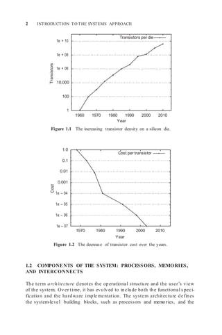
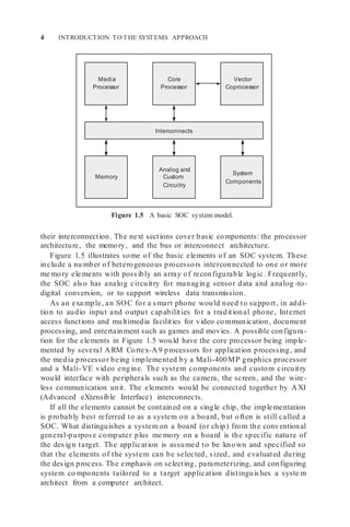
The past 40 years have seen amazing advances in silicon technology and result-
ing increases in transistor density and performance. In 1966, Fairchild
Semiconductor [84] introduced a quad two input NAND gate with about 10
transistors on a die. In 2008, the Intel quad-core Itanium processor has 2 billion
transistors [226]. Figures 1.1 and 1.2 show the unrelenting advance in improv-
ing transistor density and the corresponding decrease in device cost.
The aim of this book is to present an approach for co mputer system design
that exploits this enormous transistor density. In part, this is a direct extension
of studies in co mputer architecture and design. However, it is also a study of
system architecture and design.
About 50 years ago, a seminal text, Systems Engineering—An Introduction
to the Design of Large-Scale Systems [111], appeared. As the authors, H.H.
Goode and R.E. Machol, pointed out, the system’s view of engineering was
created by a need to deal with co mple xity. As then, our ability to deal with
complex design problems is greatly enhanced by computer-based tools.
A system-on-chip (SOC) architecture is an ensemble of processors, memo-
ries, and interconnects tailored to an application do main. A simple e xa mple
of such an architecture is the Emotion Engine [147, 187, 237] for the Sony
PlayStation 2 (Figure 1.3), which has two main functions: behavior simulation
and geometry translation. This system contains three essential components: a
main processor of the reduced instruction set computer (RISC) style [118] and
two vector processing units, VPU0 and VPU1, each of which contains four
parallel processors of the single instruction, multiple data (SIMD) stream style
[97]. We provide a brief overview of these co mponents and our overall
approach in the next few sections.
While the focus of the book is on the syste m, in order to understand the
system, one must first understand the components. So, before returning to the
issue of syste m architecture later in this chapter, we review the co mponents
that make up the system.
Computer System Design: System-on-Chip, First Edition. Michael J. Flynn and Wayne Luk.
© 2011 John Wiley & Sons, Inc. Published 2011 by John Wiley & Sons, Inc.
1](https://image.slidesharecdn.com/unit1-220410184646/85/UNIT-1-docx-1-320.jpg)
![1 Introduction to the
Systems Approach
1.1 SYSTEM ARCHITECTURE: AN OVERVIEW
The past 40 years have seen amazing advances in silicon technology and result-
ing increases in transistor density and performance. In 1966, Fairchild
Semiconductor [84] introduced a quad two input NAND gate with about 10
transistors on a die. In 2008, the Intel quad-core Itanium processor has 2 billion
transistors [226]. Figures 1.1 and 1.2 show the unrelenting advance in improv-
ing transistor density and the corresponding decrease in device cost.
The aim of this book is to present an approach for co mputer system design
that exploits this enormous transistor density. In part, this is a direct extension
of studies in co mputer architecture and design. However, it is also a study of
system architecture and design.
About 50 years ago, a seminal text, Systems Engineering—An Introduction
to the Design of Large-Scale Systems [111], appeared. As the authors, H.H.
Goode and R.E. Machol, pointed out, the system’s view of engineering was
created by a need to deal with co mple xity. As then, our ability to deal with
complex design problems is greatly enhanced by computer-based tools.
A system-on-chip (SOC) architecture is an ensemble of processors, memo-
ries, and interconnects tailored to an application do main. A simple e xa mple
of such an architecture is the Emotion Engine [147, 187, 237] for the Sony
PlayStation 2 (Figure 1.3), which has two main functions: behavior simulation
and geometry translation. This system contains three essential components: a
main processor of the reduced instruction set computer (RISC) style [118] and
two vector processing units, VPU0 and VPU1, each of which contains four
parallel processors of the single instruction, multiple data (SIMD) stream style
[97]. We provide a brief overview of these co mponents and our overall
approach in the next few sections.
While the focus of the book is on the syste m, in order to understand the
system, one must first understand the components. So, before returning to the
issue of syste m architecture later in this chapter, we review the co mponents
that make up the system.
Computer System Design: System-on-Chip, First Edition. Michael J. Flynn and Wayne Luk.
© 2011 John Wiley & Sons, Inc. Published 2011 by John Wiley & Sons, Inc.
1](https://image.slidesharecdn.com/unit1-220410184646/75/UNIT-1-docx-1-2048.jpg)
![Buffer Buffer Buffer
Branch
Prediction
Microinstructions
Hidden
Registers
COMPONENT S OF THE SYSTEM 3
Tasks synchronized with
the main processor
(behavior simulation)
Tasks synchronized with
the rendering engine
(geometry translation)
Rendering
engine
+
Arbiter
DMA (direct memory
access) path
External memory
Figure 1.3 High-level functional view of a system-on-chip: the Emotion Engine of the
Sony PlayStation 2 [147, 187].
Architecture
Implementation
Figure 1.4 The processor architecture and its implementation.
interconnection between them. The processor architecture determines the
processor’s instruction set, the associated programming model, its detailed
implementation, which may include hidden registers, branch prediction cir-
cuits and specific details concerning the ALU (arithmetic logic unit). The
implementation of a processor is also known as microarchitecture (Figure 1.4).
The system designer has a programmer’s or user’s view of the system com-
ponents, the system view of memory, the variety of specialized processors, and
www.allitebooks.com
Data Paths Control
Instruction Set
Registers
ALU
Memory
4 FP SIMD
processor
(VPU1)
4 FP SIMD
processor
(VPU0)
Main
processor
(RISC core)](https://image.slidesharecdn.com/unit1-220410184646/85/UNIT-1-docx-3-320.jpg)
![8 INTRODUCTION TO THE SYSTEMS APPROACH
Fro m the programmer’s point of view, sequential processors e xecute
one instruction at a time. However, many processors have the capability to
execute several instructions concurrently in a manner that is transparent to
the programmer, through techniques such as pipelining, multiple execution
units, and multiple cores. Pipelining is a powerful technique that is used
in almost all current processor implementations. Techniques to extract and
exploit the inherent parallelis m in the code at co mpile time or run time are
also widely used.
Exploiting program parallelism is one of the most important goals in co m-
puter architecture.
Instruction-level parallelism (ILP) means that multiple operations can be
executed in parallel within a program. ILP may be achieved with hardware,
compiler, or operating system techniques. At the loop level, consecutive loop
iterations are ideal candidates for parallel execution, provided that there is no
data dependency between subsequent loop iterations. Next, there is parallel-
ism available at the procedure level, which depends largely on the algorithms
used in the program. Finally, multiple independent programs can execute in
parallel.
Different computer architectures have been built to exploit this inherent
parallelism. In general, a computer architecture consists of one or more inter-
connected processor elements (PEs) that operate concurrently, solving a single
overall problem.
1.4.1 Processor: A Functional View
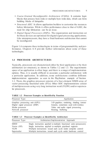
Table 1.4 shows different SOC designs and the processor used in each design.
For these exa mples, we can characterize them as general purpose, or special
purpose with support for gaming or signal processing applications. This func-
tional view tells little about the underlying hardware implementation. Indeed,
several quite different architectural approaches could implement the sa me
generic function. The graphics function, for example, requires shading, render-
ing, and texturing functions as well as perhaps a video function. Depending
TABLE 1.4 Processor Models for Different SOC Examples
SOC Application Base ISA Processor Description
Freescale e600 [101] DSP PowerPC Superscalar with
vector extension
ClearSpeed
CSX600 [59]
PlayStation 2
[147, 187, 237]
General Proprietary ISA Array processor of 96
processing elements
Gaming MIPS Pipelined with two
vector coprocessors
ARM VFP11 [23] General ARM Configurable vector
coprocessor](https://image.slidesharecdn.com/unit1-220410184646/85/UNIT-1-docx-8-320.jpg)

![PROCESSOR ARCHITECTURES 11
Control Unit
Integer FU
Instruction
Cache
Memory/L2
Data
Cache
Decode Unit
Floating-Point
FU
Data
Registers
TABLE 1.5 SOC Examples Using Pipelined Soft Processors [177, 178]. A Soft
Processor Is Implemented with FPGAs or Similar Reconfigurable Technology
Processor
Word
Length (bit)
Pipeline
Stages
I/D-Cache*
Total (KB)
Floating-
Point Unit
(FPU)
Usual
Target
Xilinx MicroBlaze 32 3 0–64 Optional FPGA
Altera Nios II fast 32 6 0–64 — FPGA
ARC 600 [19] 16/32 5 0–32 Optional ASIC
Tensilica Xtensa LX 16/24 5–7 0–32 Optional ASIC
Cambridge XAP3a 16/32 2 — — ASIC
*Means configurable I-cache and/or D-cache.
Figure 1.10 Pipelined processor model.
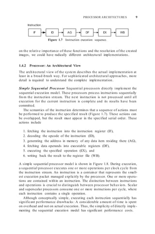
ILP While pipelining does not necessarily lead to executing multiple instruc-
tions at e xactly the same time, there are other techniques that do. These tech-
niques may use some combination of static scheduling and dynamic analysis
to perform concurrently the actual evaluation phase of several different opera-
tions, potentially yielding an execution rate of greater than one operation every
cycle. Since historically most instructions consist of only a single operation, this
kind of parallelism has been named ILP (instruction level parallelism).
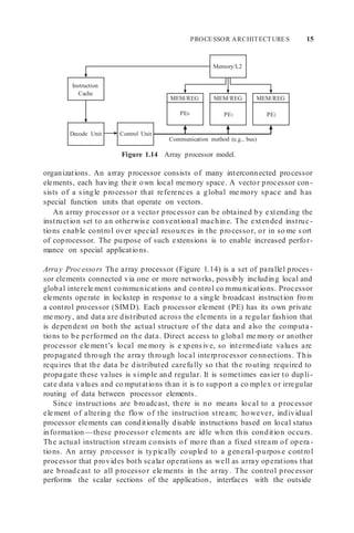
Two architectures that exploit ILP are superscalar and VLIW processors.
They use different techniques to achieve execution rates greater than one
operation per cycle. A superscalar processor dynamically examines the instruc-
tion stream to determine which operations are independent and can be e xe -
cuted. A VLIW processor relies on the co mpiler to analyze the available
operations (OP) and to schedule independent operations into wide instruc -
tion words, which then e xecute these operations in parallel with no further
analysis.
Figure 1.11 shows the instruction timing of a pipelined superscalar or VLIW
processor executing two instructions per cycle. In this case, all the instructions
are independent so that they can be executed in parallel. The next two sections
describe these two architectures in more detail.](https://image.slidesharecdn.com/unit1-220410184646/85/UNIT-1-docx-11-320.jpg)
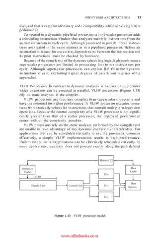
![12 INTRODUCTION TO THE SYSTEMS APPROACH
Decode Unit
Reorder
Buffer
Data
Registers
Control Unit
FU0
FU2
FU1
Rename
Buffer
IF ID AG DF EX WB
IF ID AG DF EX WB
Predecode
Instruction #1
Instruction #2
Instruction #3
Instruction #4
Instruction #5
Instruction #6
Time
Figure 1.11 Instruction timing in a pipelined ILP processor.
Figure 1.12 Superscalar processor model.
Superscalar Processors Dynamic pipelined processors re main limited to
executing a single operation per cycle by virtue of their scalar nature. This
limitation can be avoided with the addition of multiple functional units and a
dynamic scheduler to process more than one instruction per cycle (Figure
1.12). These superscalar processors [135] can achieve execution rates of several
instructions per cycle (usually limited to two, but more is possible depending
on the application). The most significant advantage of a superscalar processor
is that processing multiple instructions per cycle is done transparently to the
Data
Cache
Memory/L2
WB
EX
DF
AG
ID
IF
WB
EX
DF
AG
ID
IF
WB
EX
DF
AG
ID
IF
Instruction
Cache
EX
DF
AG
ID
IF
Dispatch
Stack
WB
.
.
.
.](https://image.slidesharecdn.com/unit1-220410184646/85/UNIT-1-docx-12-320.jpg)
![14 INTRODUCTION TO THE SYSTEMS APPROACH
by the code scheduler in the compiler. Two classes of execution variations can
arise and affect the scheduled execution behavior:
1. delayed results from operations whose latency differs from the assumed
latency scheduled by the compiler and
2. interruptions from exceptions or interrupts, which change the execution
path to a completely different and unanticipated code schedule.
Although stalling the processor can control a delayed result, this solution can
result in significant performance penalties. The most common execution delay
is a data cache miss. Many VLIW processors avoid all situations that can result
in a delay by avoiding data caches and by assuming worst -case latencies for
operations. However, when there is insufficient parallelism to hide the exposed
worst-case operation latency, the instruction schedule has many incompletely
filled or empty instructions, resulting in poor performance.
Tables 1.6 and 1.7 describe some representative superscalar and VLIW
processors.
SIMD Architectures: Array and Vector Processors The SIMD class of pro-
cessor architecture includes both array and vector processors. The SIMD pro-
cessor is a natural response to the use of certain regular data structures, such as
vectors and matrices. From the view of an assembly -level progra mmer, pro-
gramming SIMD architecture appears to be very similar to programming a
simple processor except that some operations perform computations on aggre-
gate data. Since these regular structures are widely used in scientific program-
ming, the SIMD processor has been very successful in these environments.
The two popular types of SIMD processor are the array processor and the
vector processor. They differ both in their implementations and in their data
TABLE 1.6 SOC Examples Using Superscalar Processors
Number of
Device Functional Units Issue Width Base Instruction Set
MIPS 74K Core [183] 4 2 MIPS32
Infineon TriCore2 [129] 4 3 RISC
Freescale e600 [101] 6 3 PowerPC
TABLE 1.7 SOC Examples Using VLIW Processors
Device Number of Functional Units Issue Width
Fujitsu MB93555A [103] 8 8
TI TMS320C6713B [243] 8 8
CEVA-X1620 [54] 30 8
Philips Nexperia PNX1700 [199] 30 5](https://image.slidesharecdn.com/unit1-220410184646/85/UNIT-1-docx-14-320.jpg)
![16 INTRODUCTION TO THE SYSTEMS APPROACH
TABLE 1.8 SOC Examples Based on Array Processors
Device Processors per Control Unit Data Size (bit)
ClearSpeed CSX600 [59] 96 32
Atsana J2211 [174] Configurable 16/32
Xelerator X10q [257] 200 4
world, and controls the flow of execution; the array processor performs the
array sections of the application as directed by the control processor.
A suitable application for use on an array processor has several key char-
acteristics: a significant amount of data that have a regular structure, computa-
tions on the data that are uniformly applied to many or all elements of the
data set, and simple and regular patterns relating the co mputations and the
data. An exa mple of an application that has these characteristics is the solution
of the Navier–Stokes equations, although any application that has significant
matrix co mputations is likely to benefit fro m the concurrent capabilities of an
array processor.
Table 1.8 contains several array processor examples. The ClearSpeed pro-
cessor is an exa mple of an array processor chip that is directed at signal pro-
cessing applications.
Vector Processors A vector processor is a single processor that resembles a
traditional single stream processor, except that some of the function units (and
registers) operate on vectors—sequences of data values that are seemingly
operated on as a single entity. These function units are deeply pipelined and
have high clock rates. While the vector pipelines often have higher latencies
compared with scalar function units, the rapid delivery of the input vector data
elements, together with the high clock rates, results in a significant throughput.
Modern vector processors require that vectors be explicitly loaded into
special vector registers and stored back into memory—the same course that
modern scalar processors use for similar reasons. Vector processors have
several features that enable them to achieve high performance. One feature
is the ability to concurrently load and store values between the vector register
file and the main memory while performing computations on values in the
vector register file. This is an important feature since the limited length of
vector registers requires that vectors longer than the register length would be
processed in segments—a technique called strip mining. Not being able to
overlap memory accesses and computations would pose a significant perfor-
mance bottleneck.
Most vector processors support a form of result bypassing —in this case
called chaining—that allows a follow-on co mputation to commence as soon
as the first value is available from the preceding computation. Thus, instead of
waiting for the entire vector to be processed, the follow-on computation can
be significantly overlapped with the preceding computation that it is depen -
dent on. Sequential computations can be efficiently compounded to behave as](https://image.slidesharecdn.com/unit1-220410184646/85/UNIT-1-docx-16-320.jpg)
![PROCESSOR ARCHITECTURES 17
Memory/L2
64 Vector
Registers
Data
Cache
Control Unit
Decode Unit
Instruction
Cache
Integer
Registers
FU2
FU1
FU0
if they were a single operation, with a total latency equal to the latency of the
first operation with the pipeline and chaining latencies of the remaining opera-
tions, but none of the start-up overhead that would be incurred without chain-
ing. For example, division could be synthesized by chaining a reciprocal with
a multiply operation. Chaining typically works for the results of load opera-
tions as well as normal computations.
A typical vector processor configuration (Figure 1.15) consists of a vector
register file, one vector addition unit, one vector multiplication unit, and one
vector reciprocal unit (used in conjunction with the vector multiplication unit
to perform division); the vector register file contains multiple vector registers
(elements).
Table 1.9 shows examples of vector processors. The IBM mainframes have
vector instructions (and support hardware) as an option for scientific users.
Multiprocessors Multiple processors can cooperatively e xecute to solve a
single problem by using some form of interconnection for sharing results. In
Figure 1.15 Vector processor model.
TABLE 1.9 SOC Examples Using Vector Processor
Device Vector Function Units Vector Registers
Freescale e600 [101] 4 32 Configurable
Motorola RSVP [58] 4 (64 bit partitionable at 16 bits) 2 streams (each 2 from,
1 to) memory
ARM VFP11 [23] 3 (64 bit partitionable to 32 bits) 4 × 8, 32 bit
Configurable implies a pool of N registers that can be configured as p register sets of N/p
elements.
.
.
.
.](https://image.slidesharecdn.com/unit1-220410184646/85/UNIT-1-docx-17-320.jpg)
![18 INTRODUCTION TO THE SYSTEMS APPROACH
TABLE 1.10 SOC Multiprocessors and Multithreaded Processors
Machanick IBM Cell Philips Lehtoranta
SOC [162] [141] PNX8500 [79] [155]
Number of CPUs 4 1 2 4
Threads 1 Many 1 1
Vector units 0 8 0 0
Application Various Various HDTV MPEG decode
Comment Proposal only Also called Soft processors
Viper 2
this configuration, each processor executes completely independently, although
most applications require some form of synchronization during execution to
pass information and data between processors. Since the multiple processors
share me mory and execute separate progra m tasks (MIMD [multiple instruc-
tion stream, multiple data stream]), their proper implementation is signifi-
cantly more complex then the array processor. Most configurations are
homogeneous with all processor elements being identical, although this is not
a requirement. Table 1.10 shows examples of SOC multiprocessors.
The interconnection network in the multiprocessor passes data between
processor elements and synchronizes the independent execution strea ms
between processor elements. When the memory of the processor is distributed
across all processors and only the local processor element has access to it, all
data sharing is performed explicitly using messages, and all synchronization is
handled within the message system. When the me mory of the processor is
shared across all processor elements, synchronization is more of a problem—
certainly, messages can be used through the memory system to pass data and
information between processor elements, but this is not necessarily the most
effective use of the system.
When communications between processor elements are performed through
a shared me mory address space—either global or distributed between proces-
sor ele ments (called distributed shared me mory to distinguish it fro m distrib-
uted me mory)—there are two significant problems that arise. The first is
maintaining memory consistency: the programmer-visible ordering effects on
me mory references, both within a processor ele ment and between different
processor elements. This problem is usually solved through a combination of
hardware and software techniques. The second is cache coherency —the
programmer-invisible mechanism to ensure that all processor elements see the
same value for a given memory location. This problem is usually solved exclu-
sively through hardware techniques.
The primary characteristic of a multiprocessor system is the nature of the
me mory address space. If each processor element has its own address space
(distributed me mory), the only means of communication between processor
ele ments is through message passing. If the address space is shared (shared
memory), communication is through the memory system.](https://image.slidesharecdn.com/unit1-220410184646/85/UNIT-1-docx-18-320.jpg)
![MEMORY AND ADDRESSING 21
TABLE 1.11 SOC Memory Considerations
Issue Implementation Comment
Memory placement On-die Limited and fixed size
Off-die System on a board, slow
access, limited bandwidth
Addressing Real addressing Limited size, simple OS
Virtual addressing Much more complex, require
TLB, in-order instruction
execution support
Arrangement (as programmed
for multiple processors)
Arrangement (as
implemented)
Shared memory Requires hardware support
Message passing Additional programming
Centralized Limited by chip
considerations
Distributed Can be clustered with a
processor or other
memory modules
TABLE 1.12 Memory Hierarchy for Different SOC Examples
SOC Application Cache Size
On-Die/
Off-Die
Real/
Virtual
NetSilicon NET + 40
[184]
Networking 4-KB I-cache,
4-KB D-cache
Off Real
NetSilicon NS9775 [185] Printing 8-KB I-cache,
4-KB D-cache
NXP LH7A404 [186] Networking 16-KB I-cache,
8 KB D-Cache
Off Virtual
On Virtual
Motorola RSVP [58] Multimedia Tile buffer memory Off Real
1.5.2 Addressing: The Architecture of Memory
The user’s view of memory primarily consists of the addressing facilities avail-
able to the progra mmer. Some of these facilities are available to the applica -
tion programmer and some to the operating system progra mmer. Virtual
me mory enables programs requiring larger storage than the physical me mory
to run and allows separation of address spaces to protect unauthorized access
to me mory regions when executing multiple application progra ms. When
virtual addressing facilities are properly implemented and programmed,
memory can be efficiently and securely accessed.
Virtual me mory is often supported by a me mory manage ment unit.
Conceptually, the physical memory address is determined by a sequence of (at
least) three steps:](https://image.slidesharecdn.com/unit1-220410184646/85/UNIT-1-docx-21-320.jpg)
![MEMORY AND ADDRESSING 23
Virtual Address
a
Figure 1.18 Virtual-to-real address mapping with a TLB bypass.
TABLE 1.14 Operating Systems for SOC Designs
OS Vendor Memory Model
uClinux Open source Real
VxWorks (RTOS) [254] Wind River Real
Windows CE Microsoft Virtual
Nucleus (RTOS) [175] Mentor Graphics Real
MQX (RTOS) [83] ARC Real
ality. Of primary interest to the designer is the requirement for virtual memory.
If the system can be restricted to a real me mory (physically, not virtually
addressed) and the size of the memory can be contained to the order of 10 s
of megabytes, the syste m can be implemented as a true system on a chip (all
memory on-die). The alternative, virtual memory, is often slower and signifi-
cantly more expensive, requiring a complex memory management unit. Table
1.14 illustrates some current SOC designs and their operating systems.
www.allitebooks.com
Byte in
Page
Page
Address
Segment
Table
Physical Address
TLB
User ID
Page Table](https://image.slidesharecdn.com/unit1-220410184646/85/UNIT-1-docx-23-320.jpg)
![24 INTRODUCTION TO THE SYSTEMS APPROACH
High-Speed Bus
DSP
Memory
CPU 2
CPU 1
Of course, fast real memory designs come at the price of functionality. The
user has limited ways of creating new processes and of expanding the applica-
tion base of the systems.
1.6 SYSTEM-LEVEL INTERCONNECTION
SOC technology typically relies on the interconnection of predesigned circuit
modules (known as intellectual property [IP] blocks) to form a co mplete
system, which can be integrated onto a single chip. In this way, the design task
is raised from a circuit level to a system level. Central to the syste m-level
performance and the reliability of the finished product is the method of inter-
connection used. A well-designed interconnection scheme should have vigor-
ous and efficient co mmunication protocols, una mbiguously defined as a
published standard.This facilitates interoperability between IP blocks designed
by different people fro m different organizations and encourages design reuse.
It should provide efficient communication between different modules ma xi-
mizing the degree of parallelism achieved.
SOC interconnect methods can be classified into two main approaches:
buses and network-on-chip, as illustrated in Figures 1.19 and 1.20.
1.6.1 Bus-Based Approach
With the bus-based approach, IP blocks are designed to conform to published
bus standards (such as ARM’s Advanced Microcontroller Bus Architecture
Figure 1.19 SOC system-level interconnection: bus-based approach.
Low -Speed Bus
Bus Bridge](https://image.slidesharecdn.com/unit1-220410184646/85/UNIT-1-docx-24-320.jpg)
![Routing logic
I/O controller
DSP
Memory
Memory
CPU 2
CPU 1
SYSTEM-LEVEL INTERCONNECTION 25
[AMBA] [21] or IBM’s CoreConnect [124]). Communication between modules
is achieved through the sharing of the physical connections of address, data,
and control bus signals. This is a common method used for SOC system-level
interconnect. Usually, two or more buses are employed in a system, organized
in a hierarchical fashion. To optimize system-level performance and cost, the
bus closest to the CPU has the highest bandwidth, and the bus farthest from
the CPU has the lowest bandwidth.
1.6.2 Network-on-Chip Approach
A network-on-chip system consists of an array of switches, either dynamically
switched as in a crossbar or statically switched as in a mesh.
The crossbar approach uses asynchronous channels to connect synchronous
modules that can operate at different clock frequencies. This approach has the
advantage of higher throughput than a bus -based system while making inte-
gration of a system with multiple clock domains easier.
In a simple statically switched network (Figure 1.20), each node contains
processing logic forming the core, and its own routing logic. The interconnect
scheme is based on a two-dimensional mesh topology. All co mmunications
between switches are conducted through data packets, routed through the
router interface circuit within each node. Since the interconnections between
switches have a fixed distance, interconnect -related proble ms such as wire
delay and cross talk noise are much reduced. Table 1.15 lists some interconnect
examples used in SOC designs.
Figure 1.20 SOC system-level interconnection: network-on-chip approach.](https://image.slidesharecdn.com/unit1-220410184646/85/UNIT-1-docx-25-320.jpg)
![26 INTRODUCTION TO THE SYSTEMS APPROACH
TABLE 1.15 Interconnect Models for Different SOC Examples
SOC Application Interconnect Type
ClearSpeed CSX600 [59] High Performance
Computing
ClearConnect bus
NetSilicon NET +40 [184] Networking Custom bus
NXP LH7A404 [186] Networking AMBA bus
Intel PXA27x [132] Mobile/wireless PXBus
Matsushita i-Platform [176] Media Internal connect bus
Emulex InSpeed SOC320 [130] Switching Crossbar switch
MultiNOC [172] Multiprocessing system Network-on-chip
1.7 AN APPROACH FOR SOC DESIGN
Two important ideas in a design process are figuring out the requirements and
specifications, and iterating through different stages of design toward an effi-
cient and effective completion.
1.7.1 Requirements and Specifications
Require ments and specifications are fundamental concepts in any system
design situation. There must be a thorough understanding of both before a
design can begin. They are useful at the beginning and at the end of the design
process: at the beginning, to clarify what needs to be achieved; and at the end,
as a reference against which the completed design can be evaluated.
The system require ments are the largely e xternally generated criteria for
the system. They may come from competition, from sales insights, from cus -
tomer requests, from product profitability analysis, or fro m a combination.
Require ments are rarely succinct or definitive of anything about the syste m.
Indeed, requirements can frequently be unrealistic: “I want it fast, I want it
cheap, and I want it now!”
It is important for the designer to analyze carefully the require ments
expressions, and to spend sufficient time in understanding the market situation
to determine all the factors expressed in the requirements and the priorities
those factors imply. Some of the factors the designer considers in determining
requirements include
• compatibility with previous designs or published standards,
• reuse of previous designs,
• customer requests/complaints,
• sales reports,
• cost analysis,
• competitive equipment analysis, and
• trouble reports (reliability) of previous products and competitive
products.](https://image.slidesharecdn.com/unit1-220410184646/85/UNIT-1-docx-26-320.jpg)
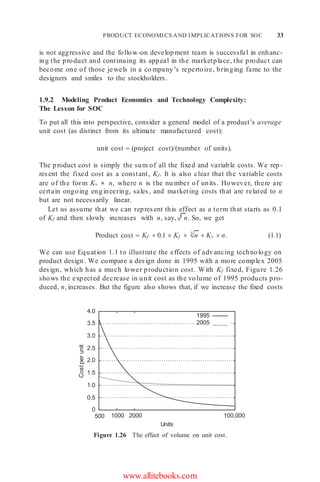
![PRODUCT ECONOMICS AND IMPLICATIONS FOR SOC 31
Manufacturing
costs
Product cost
Even when the SOC approach is technically attractive, it has economic limita-
tions and implications. Given the processor and interconnect co mplexity, if
we limit the usefulness of an implementation to a particular application, we
have to either (1) ensure that there is a large market for the product or (2)
find methods for reducing the design cost through design reuse or similar
techniques.
1.9 PRODUCT ECONOMICS AND IMPLICATIONS FOR SOC
1.9.1 Factors Affecting Product Costs
The basic cost and profitability of a product depend on many factors: its tech-
nical appeal, its cost, the market size, and the effect the product has on future
products. The issue of cost goes well beyond the product’s manufacturing cost.
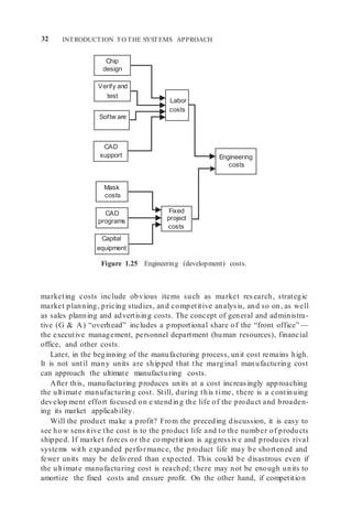
There are fixed and variable costs, as shown in Figure 1.24. Indeed, the
engineering costs, frequently the largest of the fixed costs, are expended before
any revenue can be realized from sales (Figure 1.25).
Depending on the complexity, designing a new chip requires a development
effort of anywhere between 12 and 30 months before the first manufactured
unit can be shipped. Even a moderately sized project may require up to 30 or
more hardware and software engineers, CAD design, and support personnel.
For instance, the paper describing the Sony Emotion Engine has 22 authors
[147, 187]. However, their salary and indirect costs might represent only a
fraction of the total development cost.
Nonengineering fixed costs include manufacturing start-up costs, inven-
tory costs, initial marketing and sales costs, and administrative overhead. The
Fixed
costs
Variable costs
Marketing,
sales,
administration
Engineering
Figure 1.24 Project cost components.](https://image.slidesharecdn.com/unit1-220410184646/85/UNIT-1-docx-31-320.jpg)
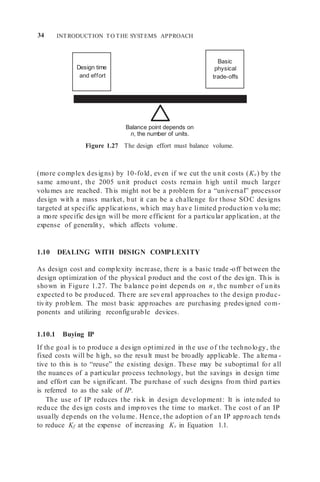
![CONCLUSIONS 37
3. FPGAs can be used for rapid prototyping of circuits that would be fab -
ricated. In this approach, one or more FPGAs are configured according
to the proposed design to emulate it, as a form of “in-circuit emulation.”
Programs are run and design errors can be detected.
4. The reconfigurability of FPGAs enables in -system upgrade, which helps
to increase the time in market of a product; this capability is especially
valuable for applications where new functions or new standards tend to
emerge rapidly.
5. The FPGA can be configured to suit a portion of a task and then recon -
figured for the remainder of the task (called “run-time reconfiguration”).
This enables specialized functional units for certain computations to
adapt to environmental changes.
6. In a number of compute-intensive applications, FPGAs can be config -
ured as a very efficient systolic co mputational array. Since each FPGA
cell has one or more storage elements, co mputations can be pipelined
with very fine granularity. This can provide an enormous computational
bandwidth, resulting in impressive speedup on selected applications.
So me devices, such as the Stretch S5 software configurable processor,
couple a conventional processor with an FPGA array [25].
Reconfiguration and FPGAs play an important part in efficient SOC design.
We shall explore them in more detail in the next chapter.
1.11 CONCLUSIONS
Building modern processors or targeted application systems is a complex
undertaking. The great advantages offered by the technology—hundreds of
millions of transistors on a die—comes at a price, not the silicon itself, but the
enormous design effort that is required to implement and support the product.
There are many aspects of SOC design, such as high-level descriptions,
compilation technologies, and design flow, that are not mentioned in this
chapter. Some of these will be covered later.
In the following chapters, we shall first take a closer look at basic trade -offs
in the technology: time, area, power, and reconfigurability. Then, we shall look
at some of the details that make up the system components: the processor, the
cache, and the memory, and the bus or switch interconnecting them. Next, we
cover design and implementation issues from the perspective of customization
and configurability. This is followed by a discussion of SOC design flow and
application studies. Finally, some challenges facing future SOC technology are
presented.
The goal of the text is to help system designers identify the most efficient
design choices, together with the mechanisms to manage the design complexity
by exploiting the advances in technology.](https://image.slidesharecdn.com/unit1-220410184646/85/UNIT-1-docx-37-320.jpg)
![38 INTRODUCTION TO THE SYSTEMS APPROACH
1.12 PROBLEM SET
1. Suppose the TLB in Figure 1.18 had 256 entries (directly addressed). If
the virtual address is 32 bits, the real memory is 512 MB and the page size
is 4 KB, show the possible layout of a TLB entry. What is the purpose of
the user ID in Figure 1.18 and what is the consequence of ignoring it?
2. Discuss possible arrangement of addressing the TLB.
3. Find an actual VLIW instruction format. Describe the layout and the con -
straints on the program in using the applications in a single instruction.
4. Find an actual vector instruction for vector ADD. Describe the instruction
layout. Repeat for vector load and vector store. Is overlapping of vector
instruction execution permitted? Explain.
5. For the pipelined processor in Figure 1.9, suppose instruction #3 sets the
CC (condition code that can be tested by following a branch instruction)
at the end of WB and instruction #4 is the condition branch. Without
additional hardware support, what is the delay in executing instruction #5
if the branch is taken and if the branch is not taken?
6. Suppose we have four different processors; each does 25% of the applica -
tion. If we improve two of the processors by 10 times, what would be the
overall application speedup?
7. Suppose we have four different processors and all but one are totally
limited by the bus. If we speed up the bus by three times and assume the
processor performance also scales, what is the application speedup?
8. For the pipelined processor in Figure 1.9, assume the cache miss rate is
0.05 per instruction execution and the total cache miss delay is 20 cycles.
For this processor, what is the achievable cycle per instruction (CPI)?
Ignore other delays, such as branch delays.
9. Design validation is a very important SOC design consideration. Find
several approaches specific to SOC designs. Evaluate each from the per -
spective of a small SOC vendor.
10. Find (from the Internet) two new VLIW DSPs. Determine the ma ximu m
number of operations issued in each cycle and the makeup of the opera -
tions (nu mber of integer, floating point, branch, etc.). What is the stated
ma ximu m performance (operations per second)? Find out how this
number was computed.
11. Find (from the Internet) two new, large FPGA parts. Determine the
number of logic blocks (configurable logic blocks [CLBs]), the minimum
cycle time, and the ma ximu m allowable power consu mption. What soft
processors are supported?](https://image.slidesharecdn.com/unit1-220410184646/85/UNIT-1-docx-38-320.jpg)