Download as PDF, PPTX
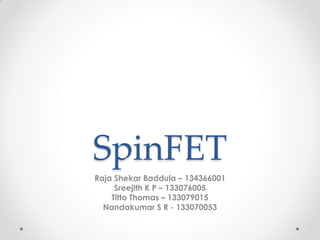
![Spin-Orbit interaction
Heterojunction:
Atomic case
Enucleus
ˆ
Ze r
4 0 r 2
AlGaAs
j Zev
InGaAs
In analogy with the atomic
case Rashba S-O term
In Electron rest frame
Amperes' law
B
0 j r
4 r 2
E
Beff 0 0 (v Enucleus )
S O spin Beff
H S O
g B S
(v E )
2
hc
g B
( p V )
2
2mc
,k x ,k
k y
k
,k y ,k
,k z ,k 0
EE733 : SpinFET
kx
k
dV
ˆ
V z
g B dz
dV
H S O
[ ( p z
)]
2
2mc
dz
g B
dV
H S O
[z
( p)]
2
2mc
dz
H S O
[ z ( p)]
h
1
2
2
H
( px p y ) ( x p y y px )
2m
h
3](https://image.slidesharecdn.com/spinfet-131216080557-phpapp02/85/SpinFET-3-320.jpg)


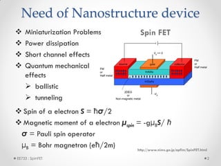
![Channel Requirements
2DEGs in narrow band gap semiconductor
Ballistic tranport
Avoid spin relaxation[1]
Elliot Yafet
[2]
D'yakonov-Perl
Bir-Aronov-Pikus
[1] J. Fabian and S. Das Sarma, Spin relaxation of conduction electrons, 1993
[2] Satoshi Sugahara and Junsaku Nitta, Spin-Transistor Electronics: An Overview and Outlook, 2010
EE733 : SpinFET
10](https://image.slidesharecdn.com/spinfet-131216080557-phpapp02/85/SpinFET-10-320.jpg)
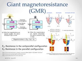
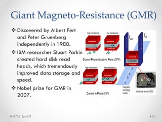
![Electrostatic control of spin
Aharonov – Bohm
Experiment [1]
Conductance
[2]
variation
Phase difference in the
Applied potential controls
the polarization of the
electron
wave vector
𝟐 𝒎∗ 𝜼𝒍
∆𝜽 =
ћ𝟐
[1] J. Nitta, F. E. Meijer, and H. Takayanagi, Spin-interference device, 1999
[2] Satoshi Sugahara and Junsaku Nitta, Spin-Transistor Electronics: An Overview and Outlook, 2010
EE733 : SpinFET
11](https://image.slidesharecdn.com/spinfet-131216080557-phpapp02/85/SpinFET-11-320.jpg)
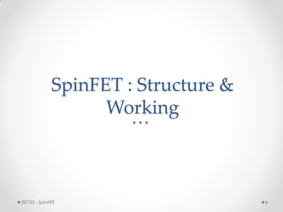
![Non-ballistic SpinFET
Scattering tolerent
Dresselhaus spin-orbit
coupling
Making both the
coefficients equal
[1]
J. Schliemann, J. C. Egues, and D. Loss, Nonballistic spin-field-effect transistor, 2003
[1] Satoshi Sugahara and Junsaku Nitta, Spin-Transistor Electronics: An Overview and Outlook, 2010
EE733 : SpinFET
13](https://image.slidesharecdn.com/spinfet-131216080557-phpapp02/85/SpinFET-13-320.jpg)
![SpinFET improvemts
Improvements
[1]
Holes as carriers
Strain engineering to shift the hole subbands
Modified device structure
Gate control hinderance [2]
Fano resonance
Ramsauer resonance
Dual gate as an option
[1] D. M. Gvozdie, U. Ekenberg, and I. Thylen, Comparison of performance of spin transistors with conventional transistors, 2005
[2] J. Wan, M. Cahay, and S. Bandyopadhyay, Proposal for a dual-gate spin field effect transistor: A device with very small
switching voltage and a large ON to OFF conductance ratio, 2008
EE733 : SpinFET
14](https://image.slidesharecdn.com/spinfet-131216080557-phpapp02/85/SpinFET-14-320.jpg)


The document discusses Spin Field Effect Transistors (SpinFETs), focusing on their structure, working principles, and applications in memory and logic devices. Key concepts include electron spin, spin injection, and giant magnetoresistance, along with advancements in semiconductor technologies. The importance of controlling spin and polarization through electrostatic means is highlighted, along with potential future developments in spintronics.


