Downloaded 177 times


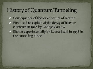

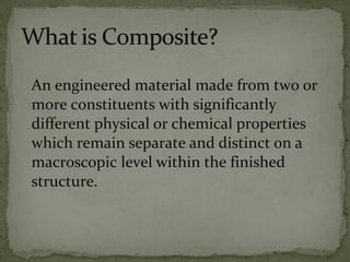
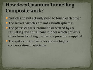


This document discusses quantum tunneling and quantum tunneling composite materials. It begins with an overview of quantum tunneling and how it allows particles to pass through barriers they classically could not. It then describes quantum tunneling composite materials, which use the quantum tunneling effect to create sensors. When flexed, the materials change from insulators to conductors, allowing them to detect forces. The document discusses several potential applications of these new quantum tunneling composite sensors in areas like toys, sports, medicine, tools, robotics and keyboards.