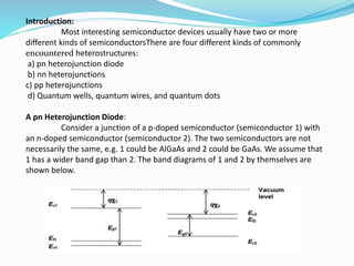
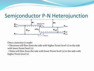
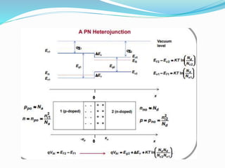
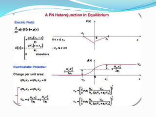
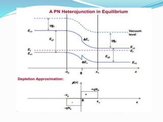
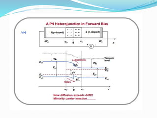
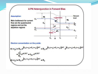
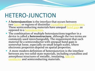
The document discusses heterojunctions and p-n junctions. It defines a heterojunction as the interface between two dissimilar semiconductors with different band gaps. There are three types of heterojunctions based on band alignment: type I where bands straddle, type II where bands are staggered, and type III where there is a broken gap. A p-n heterojunction diode forms when a p-doped and n-doped semiconductor meet; electrons flow from the higher to lower Fermi level side and holes in the opposite direction.

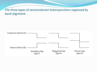
![ENERGY BAND ALIGNMENT
The behaviour of a semiconductor junction depends
crucially on the alignment of the energy bands at the
interface. Semiconductor interfaces can be organized
into three types of heterojunctions: straddling gap
(type I), staggered gap (type II) or broken gap (type
III) as seen in the figure[9]. Away from the junction,
the band bending can be computed based on the
usual procedure of solving Poisson's equation.](https://image.slidesharecdn.com/hetero-junction-200202153801/85/Hetero-junction-3-320.jpg)