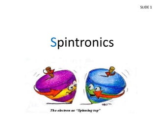
Spintronics 
SLIDE 1
Introduction 
 Conventional electronic 
devices ignore the spin 
property and rely strictly on 
the transport of the electrical 
charge of electrons 
 Adding the spin degree of 
freedom provides new effects, 
new capabilities and new 
functionalities 
SLIDE 2
Future Demands 
 Moore’s Law states that the number of 
transistors on a silicon chip will roughly 
double every eighteen months 
 As electronic devices become smaller, 
quantum properties of the wavelike nature 
of electrons are no longer negligible 
 Spintronic devices offer the possibility of 
enhanced functionality, higher speed, and 
reduced power consumption 
SLIDE 3
Spintronics = Spin-based electronics 
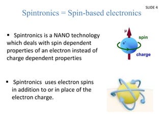
 Spintronics is a NANO technology 
which deals with spin dependent 
properties of an electron instead of 
charge dependent properties 
 Spintronics uses electron spins 
in addition to or in place of the 
electron charge. 
SLIDE 4
Principle 
 Every electron exist in one of the two states spin-up 
and spin-down, with spins either positive half or 
negative half. 
SLIDE 5 
 Origin of the spin is electron’s intrinsic property 
“angular momentum” 
 Spin is a characteristic that makes an electron a 
tiny magnet with north and south poles. 
 The orientation of north-south axis depends on the 
particle’s axis of spin.
Principle 
 In other words, electrons can rotate either clock 
wise or anti-clockwise around its own axis with 
constant frequency. 
 The two possible spin states represent ‘0’and‘1’ 
in logical operations. 
 In ordinary materials, the up magnetic moments 
cancel the down magnetic moment so no surplus 
moment piles up. 
 Ferro-magnetic materials like iron, cobalt and 
nickel is needed for designing of spin electronic 
devices. 
SLIDE 6
Principle 
SLIDE 7 
1. These have tiny regions called domains in 
which an excess of electrons have spins with 
axis pointing either up or down. 
2. The domains are randomly scattered and 
evenly divided between majority-up and 
majority-down. 
3. But, an externally applied magnetic field will 
line up the domains in the direction of the 
field. This results in a permanent magnet.
Gaint Magnetoresistance (GMR) 
SLIDE 8 
 The basic GMR device consists of a layer of non -magnetic metal 
between two magnetic layers. 
 A current consisting of spin-up and spin-down electrons is passed through 
the layers. 
 Those oriented in the same direction as the electron spins in a magnetic 
layer pass through quite easily while those oriented in the opposite direction 
are scattered.
Advantage Of Spintronics 
 Low power consumption. 
 Less heat dissipation. 
 Spintronic memory is non-volatile. 
 Takes up lesser space on chip, thus more compact. 
 Spin manipulation is faster , so greater read & write speed. 
 Spintronics does not require unique and specialized 
semiconductors. 
Common metals such as Fe, Al, Ag , etc. can be used. 
SLIDE 9
Applications 
Spin Polarized Feild Effect 
Transistor (Spin-FET) 
SLIDE 9 
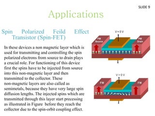
In these devices a non magnetic layer which is 
used for transmitting and controlling the spin 
polarized electrons from source to drain plays 
a crucial role. For functioning of this device 
first the spins have to be injected from source 
into this non-magnetic layer and then 
transmitted to the collector. These 
non-magnetic layers are also called as 
semimetals, because they have very large spin 
diffusion lengths. The injected spins which are 
transmitted through this layer start precessing 
as illustrated in Figure before they reach the 
collector due to the spin-orbit coupling effect.
2. MRAM 
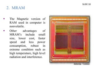
 The Magnetic version of 
RAM used in computer is 
nonvolatile. 
 Other advantages of 
MRAM’s include small 
size, lower cost, faster 
speed and less power 
consumption, robust in 
extreme condition such as 
high temperature, high level 
radiation and interference. 
SLIDE 10
MRAM SLIDE 11 
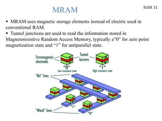
 MRAM uses magnetic storage elements instead of electric used in 
conventional RAM. 
 Tunnel junctions are used to read the information stored in 
Magnetoresistive Random Access Memory, typically a”0” for zero point 
magnetization state and “1” for antiparallel state.
MRAM 
Magneto resistive RAM 
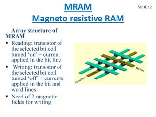
Array structure of 
MRAM 
 Reading: transistor of 
the selected bit cell 
turned ‘on’ + current 
applied in the bit line 
 Writing: transistor of 
the selected bit cell 
turned ‘off’ + currents 
applied in the bit and 
word lines 
 Need of 2 magnetic 
fields for writing 
SLIDE 12
SLIDE 13 
This technology will exploit the spin of the 
electron and create new devices and circuits which could 
be more beneficial in future by providing devices like 
memories for data base accessing with the speed of light. 
The devices of this technology are very useful for 
transaction processing and for scientific number 
crunching. 
Moreover, these "spintronic" devices might lead 
to quantum computers and quantum communication 
based on electronic solid-state devices, thus changing the 
perspective of information technology in the 21st century
 spintronics

spintronics

  • 1.
  • 2.
    Introduction  Conventionalelectronic devices ignore the spin property and rely strictly on the transport of the electrical charge of electrons  Adding the spin degree of freedom provides new effects, new capabilities and new functionalities SLIDE 2
  • 3.
    Future Demands Moore’s Law states that the number of transistors on a silicon chip will roughly double every eighteen months  As electronic devices become smaller, quantum properties of the wavelike nature of electrons are no longer negligible  Spintronic devices offer the possibility of enhanced functionality, higher speed, and reduced power consumption SLIDE 3
  • 4.
    Spintronics = Spin-basedelectronics  Spintronics is a NANO technology which deals with spin dependent properties of an electron instead of charge dependent properties  Spintronics uses electron spins in addition to or in place of the electron charge. SLIDE 4
  • 5.
    Principle  Everyelectron exist in one of the two states spin-up and spin-down, with spins either positive half or negative half. SLIDE 5  Origin of the spin is electron’s intrinsic property “angular momentum”  Spin is a characteristic that makes an electron a tiny magnet with north and south poles.  The orientation of north-south axis depends on the particle’s axis of spin.
  • 6.
    Principle  Inother words, electrons can rotate either clock wise or anti-clockwise around its own axis with constant frequency.  The two possible spin states represent ‘0’and‘1’ in logical operations.  In ordinary materials, the up magnetic moments cancel the down magnetic moment so no surplus moment piles up.  Ferro-magnetic materials like iron, cobalt and nickel is needed for designing of spin electronic devices. SLIDE 6
  • 7.
    Principle SLIDE 7 1. These have tiny regions called domains in which an excess of electrons have spins with axis pointing either up or down. 2. The domains are randomly scattered and evenly divided between majority-up and majority-down. 3. But, an externally applied magnetic field will line up the domains in the direction of the field. This results in a permanent magnet.
  • 8.
    Gaint Magnetoresistance (GMR) SLIDE 8  The basic GMR device consists of a layer of non -magnetic metal between two magnetic layers.  A current consisting of spin-up and spin-down electrons is passed through the layers.  Those oriented in the same direction as the electron spins in a magnetic layer pass through quite easily while those oriented in the opposite direction are scattered.
  • 9.
    Advantage Of Spintronics  Low power consumption.  Less heat dissipation.  Spintronic memory is non-volatile.  Takes up lesser space on chip, thus more compact.  Spin manipulation is faster , so greater read & write speed.  Spintronics does not require unique and specialized semiconductors. Common metals such as Fe, Al, Ag , etc. can be used. SLIDE 9
  • 10.
    Applications Spin PolarizedFeild Effect Transistor (Spin-FET) SLIDE 9 In these devices a non magnetic layer which is used for transmitting and controlling the spin polarized electrons from source to drain plays a crucial role. For functioning of this device first the spins have to be injected from source into this non-magnetic layer and then transmitted to the collector. These non-magnetic layers are also called as semimetals, because they have very large spin diffusion lengths. The injected spins which are transmitted through this layer start precessing as illustrated in Figure before they reach the collector due to the spin-orbit coupling effect.
  • 11.
    2. MRAM The Magnetic version of RAM used in computer is nonvolatile.  Other advantages of MRAM’s include small size, lower cost, faster speed and less power consumption, robust in extreme condition such as high temperature, high level radiation and interference. SLIDE 10
  • 12.
    MRAM SLIDE 11  MRAM uses magnetic storage elements instead of electric used in conventional RAM.  Tunnel junctions are used to read the information stored in Magnetoresistive Random Access Memory, typically a”0” for zero point magnetization state and “1” for antiparallel state.
  • 13.
    MRAM Magneto resistiveRAM Array structure of MRAM  Reading: transistor of the selected bit cell turned ‘on’ + current applied in the bit line  Writing: transistor of the selected bit cell turned ‘off’ + currents applied in the bit and word lines  Need of 2 magnetic fields for writing SLIDE 12
  • 14.
    SLIDE 13 Thistechnology will exploit the spin of the electron and create new devices and circuits which could be more beneficial in future by providing devices like memories for data base accessing with the speed of light. The devices of this technology are very useful for transaction processing and for scientific number crunching. Moreover, these "spintronic" devices might lead to quantum computers and quantum communication based on electronic solid-state devices, thus changing the perspective of information technology in the 21st century

Editor's Notes

  • #3 Spin does not replace charge current just provide extra control Using suitable materials, many different “bit” states can be interpreted
  • #4 New technology has been proposed which would involve a complete set of new materials, new handling and processing techniques, and altered circuit design. Such developments include single-electron transistors and molecular-electronic devices based on organic materials or carbon nanotubes.