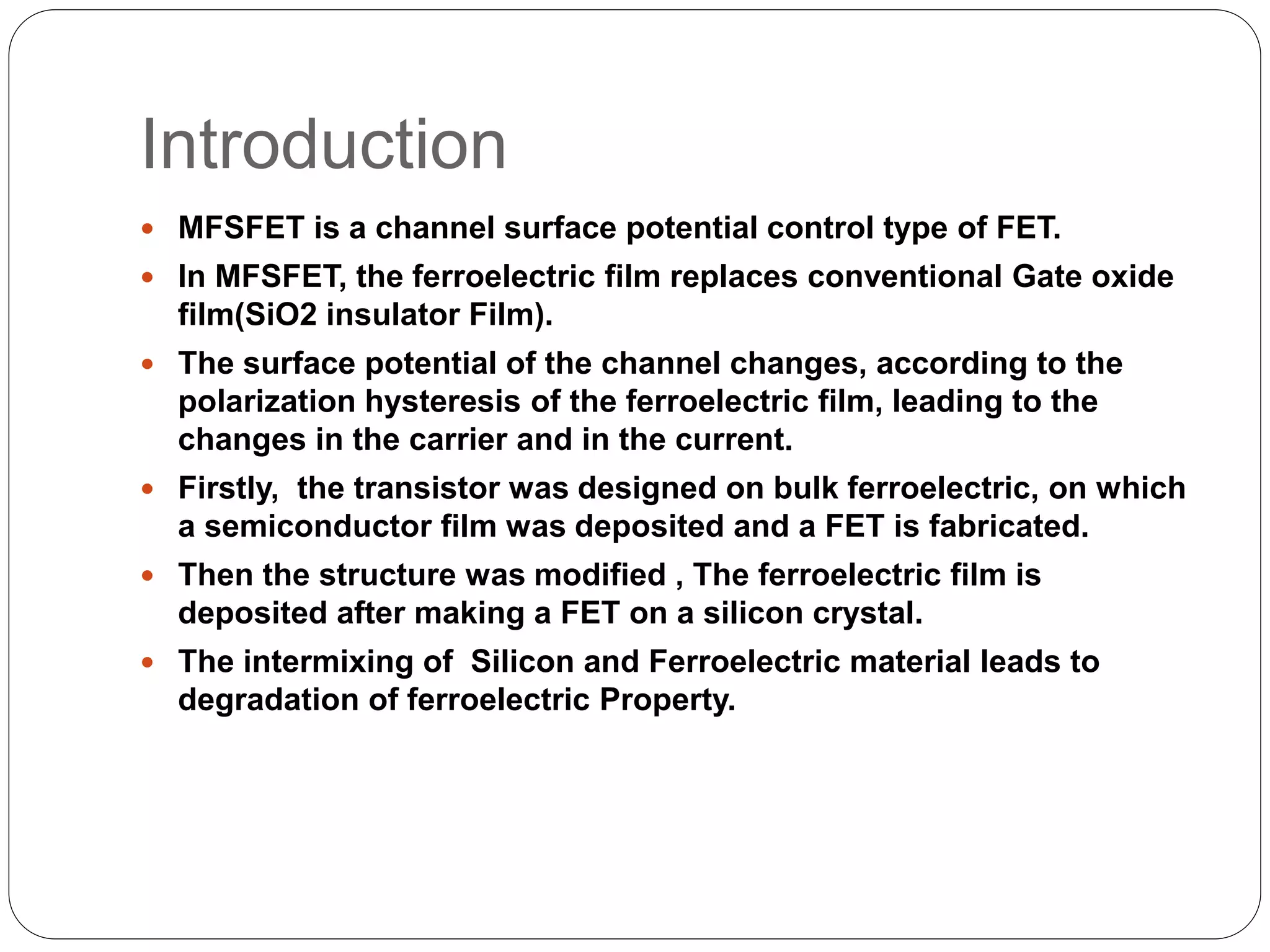
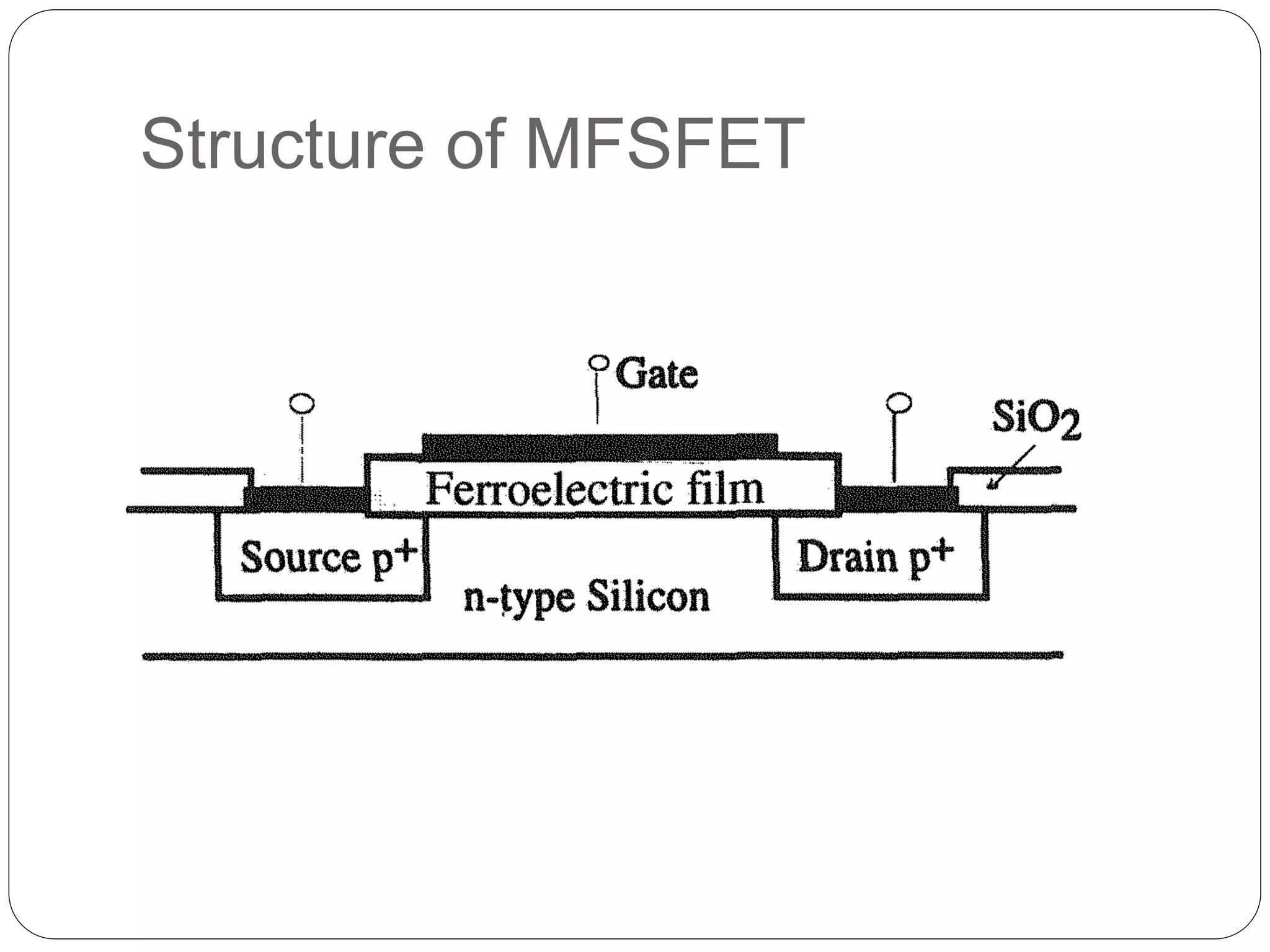
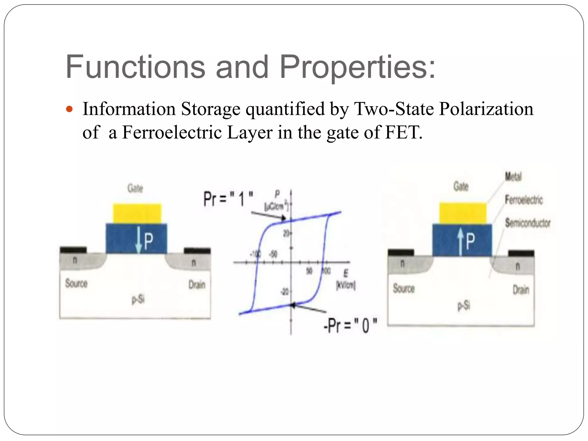
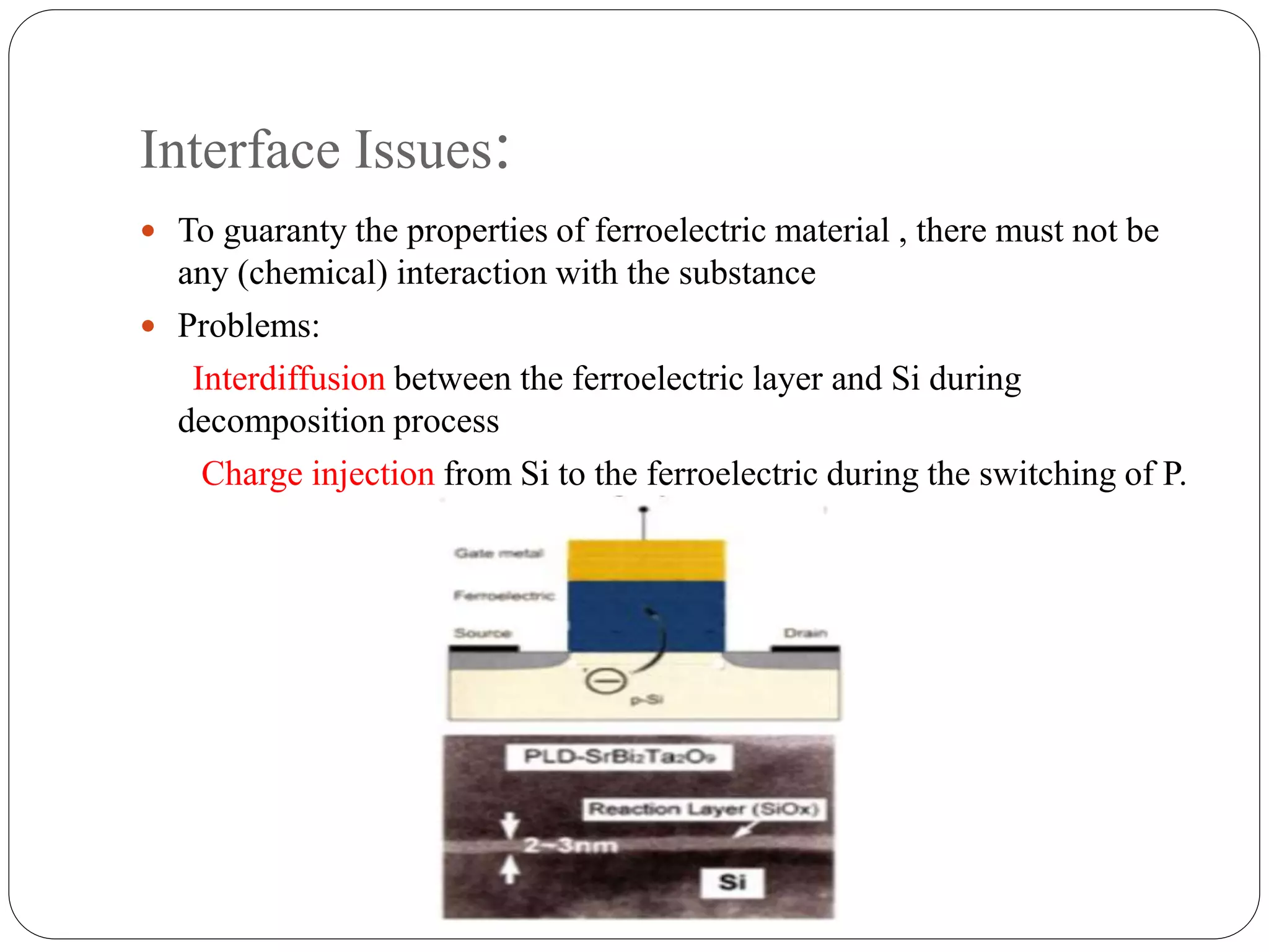
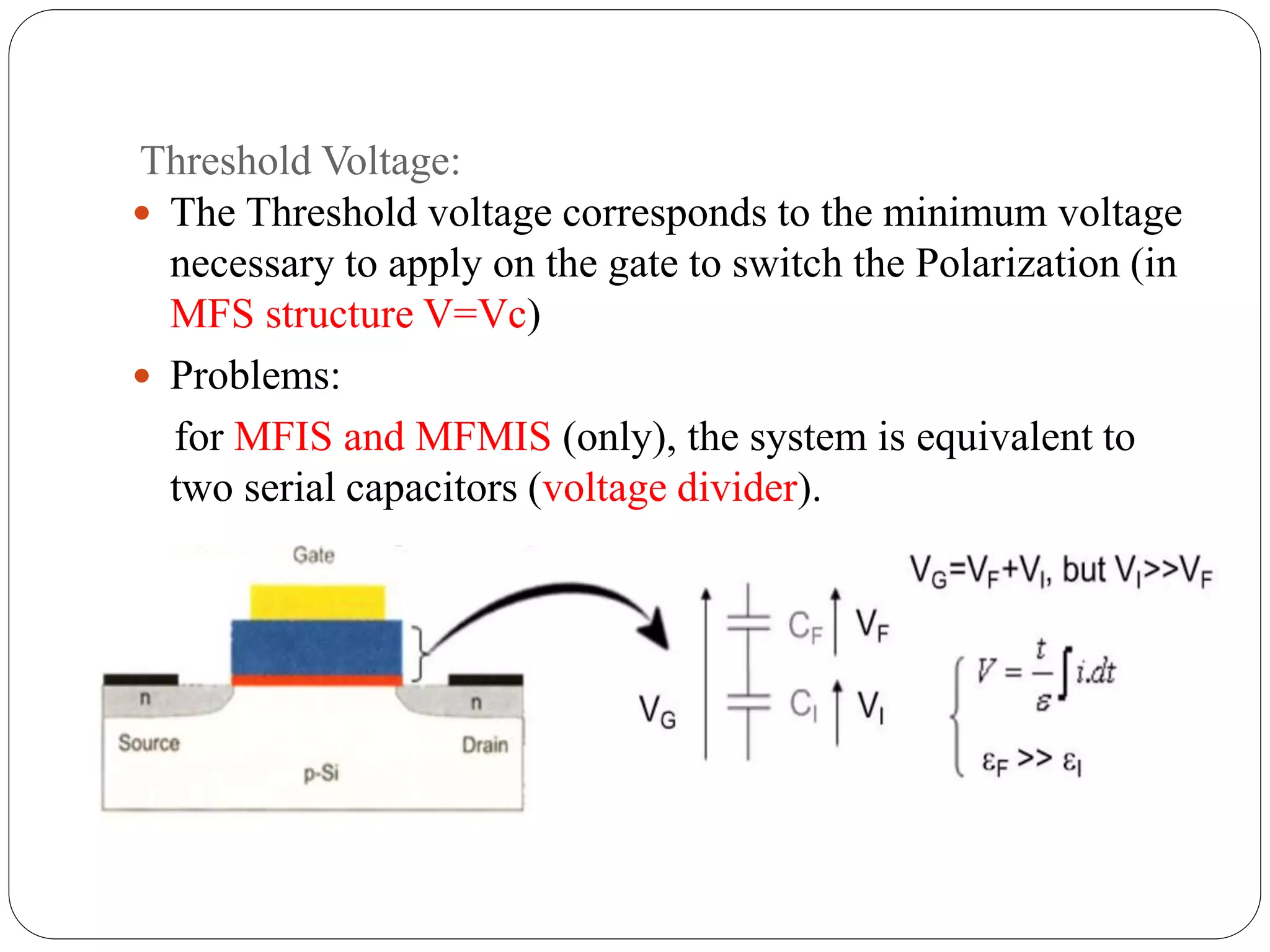
2. Introduction
MFSFET is a channel surface potential control type of FET.
In MFSFET, the ferroelectric film replaces conventional Gate oxide
film(SiO2 insulator Film).
The surface potential of the channel changes, according to the
polarization hysteresis of the ferroelectric film, leading to the
changes in the carrier and in the current.
Firstly, the transistor was designed on bulk ferroelectric, on which
a semiconductor film was deposited and a FET is fabricated.
Then the structure was modified , The ferroelectric film is
deposited after making a FET on a silicon crystal.
The intermixing of Silicon and Ferroelectric material leads to
degradation of ferroelectric Property.
4. Functions and Properties:
Information Storage quantified by Two-State Polarization
of a Ferroelectric Layer in the gate of FET.
5. Properties:
Non-Volatile , due to Remnant Polarization (Pr).
Non-Destructive Reading , as it is measure of resistance.
Fast (~20 ns, compared to flash memory ~100µs), due to
physical process of Polarization switching.
Non-Volatile Writing Process:
• Data stored in the orientation of the polarization P
• By Applying Electric Field (gate Voltage) higher than the
coercive Field Ec (|V|>|Vc|).
•After turning off the power, P becomes equal to Pr.
6.
7. Non-Destructive Reading Process:
Due to polarization, Charges appear at the interface of F/Si
Those charges influence the resistivity of the FET channel.
The reading is processed by measuring this resistivity.
8. Requirements:
Compatibility With CMOS Technology
Integration of the material without the change of
ferroelectric properties.
No retention Loss
conservation of the polarization Pr (more than 10
years).
Easily Switchable
Switch must be fast and not need much power.
High Cycle Endurance
More than 10^15 writing processes.
10. Interface Issues:
To guaranty the properties of ferroelectric material , there must not be
any (chemical) interaction with the substance
Problems:
Interdiffusion between the ferroelectric layer and Si during
decomposition process
Charge injection from Si to the ferroelectric during the switching of P.
11. Solution Proposed:
New Deposition Technique (eg: Molecular Beam Epitaxy)
To Isolate the ferroelectric material: MFIS and MFMIS
Structure.
12. Threshold Voltage:
The Threshold voltage corresponds to the minimum voltage
necessary to apply on the gate to switch the Polarization (in
MFS structure V=Vc)
Problems:
for MFIS and MFMIS (only), the system is equivalent to
two serial capacitors (voltage divider).
13. Solution Proposed:
The Voltage drop is reduced using High ξ insulator.
Retention Time:
The polarization should stay oriented in the same direction.
Problems:
For MFIS and MFMIS (only), apparition of an electric field opposed
to the polarization.
Ferroelectric Materials with a low Vc shows unstable polarization.
14. Solution Proposed:
1.Buffer layer: High Capacitance ( high ξ material or low
thickness).
2. Ferroelectrics : low remnant polarization Pr.
3.(MFMIS)M/F layer surface smaller than M/I.
4. Better Stability : Large thickness ferroelectric layer are used.
15. Fatigue effect
After several millions of switching , the remnant
polarization must be unchanged.
Problems:
Polarization (Pr) decreases with increasing
number of cycles ( reduction of 50% after 10^12
cycles).
No distinction between On and Off states.
17. Literature Review:
A ferroelectric semiconductor field-effect transistor
Ferroelectric field-effect transistors employ a ferroelectric material as a gate
insulator, the polarization state of which can be detected using the channel
conductance of the device. As a result, the devices are potentially of use in non-
volatile memory technology, but they suffer from short retention times, which limits
their wider application.
we report a ferroelectric semiconductor field-effect transistor in which a
two-dimensional ferroelectric semiconductor, indium selenide (α-In2Se3), is
used as the channel material in the device. α-In2Se3 was chosen due to its
appropriate bandgap, room-temperature ferroelectricity , ability to
maintain ferroelectricity down to a few atomic layers and its potential for
large-area growth. A passivation method based on the atomic layer
deposition of aluminium oxide (Al2O3) was developed to protect and
enhance the performance of the transistors. With 15-nm-thick hafnium
oxide (HfO2) as a scaled gate dielectric, the resulting devices offer high
performance with a large memory window, a high on/off ratio of over 108, a
maximum on current of 862 μA μm−1 and a low supply voltage.
18.
19. Ferroelectric field effect transistors: Progress and perspective
In this article, the basic principles of the FeFET and the design
strategies for state-of-the-art FeFETs will be discussed. FeFETs
using Pb(ZrxTi1−x)O3, polyvinylidene fluoride, HZO, and two-
dimensional materials are emphasized. FeFETs, ferroelectric
semiconductor field effect transistors, and metal–ferroelectric–
insulator–semiconductor structures to which those materials can be
applied are introduced, and their exotic performances are
investigated. Finally, the limitations of these devices current
performance and the potential of these materials are presented.