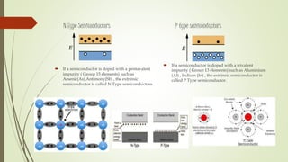
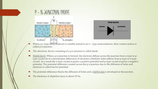
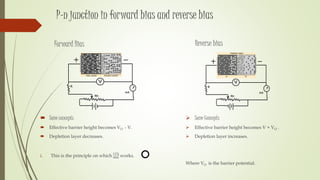
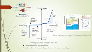
SlideShare a Scribd company logo
Semiconductors
& Leds
By Akash Ganguly
b.Tech. polymer science
Roll no. : 1308031
Index
 Semiconductors
 Concept of Energy bands
 intrinsic and extrinsic semiconductors
 Concept of electrons and holes
 N Type Semiconductors
 P type semiconductors
 P – N JUNCTION DIODE
 P-n junction in forward bias and reverse bias
 Graph for p-n junction at forward and reverse bias
 LIGHT EMITTING DIODE ( led)
 Major contributions of various scientists on LEDS
 Research on Use of LED in place of incandescent lamps!!!
 Basic Advantages of led light
 Disadvantages of leds
Semiconductors
 A semiconductor is a material which has electrical conductivity to a degree between that of a conductors
(such as copper) and that of an insulator (such as glass).
 They have resistivity or conductivity intermediate to metals and insulators.
ρ ~ 10-5 – 106Ohm m
~ 105 – 10 -6 Sm-1
 Semiconductors are the foundation of modern electronics, including transistors, solar cells, light-emitting
diodes (LEDs), quantum dots and digital and analog integrated circuits.
Concept of Energy bands
 The group of discrete but closely spaced energy levels for the orbital electrons in the atoms is called
energy band.
o The upper empty energy band is called conduction band and the lower completely filled energy band is
called valence band. In between there is a group of energy levels which cannot be occupied by the
electrons and hence called the forbidden band. Electrons can jump to the conduction band from the
valence band without stopping in the forbidden band.
o The difference of energy between the conduction band and the valence band is forbidden energy gap (Eg).
 For Silicon Eg = 1.1eV and for Germanium Eg = 0.7eV
Fermi Energy level
It is the maximum energy that an electron in the valence band
possesses at absolute zero is called Fermi energy and the level
corresponding to it is called Fermi Energy level.
Intrinsic semiconductor.
 intrinsic and extrinsic semiconductors
 A pure semiconductor is called
 To increase the electrical conductivity the semiconductor is mixed with either pentavalent impurity (
Group 15) or trivalent impurity ( Group 13). The process is called doping. The doped semiconductor is
called Extrinsic semiconductor.
 Generally one impurity atom is added for about 108 atoms of the semiconductor.
Concept of electrons and holes
 When temperature rises, an electrons jumps from the valence band and jumps to the conduction
band a vacancy is created in the valence band. This vacancy is called hole. For an intrinsic
semiconductor the sample is electrically neutral and the number of free electrons is equal to the
number of holes in the valence band.
N Type Semiconductors
 If a semiconductor is doped with a pentavalent
impurity ( Group 15 elements) such as
Arsenic(As),Antimony(Sb) , the extrinsic
semiconductor is called N Type semiconductors.
P type semiconductors
 If a semiconductor is doped with a trivalent
impurity ( Group 13 elements) such as Aluminium
(Al) , Indium (In) , the extrinsic semiconductor is
called P Type semiconductor.
P – N JUNCTION DIODE
 When a p –type semiconductor is suitably joined to an n – type semiconductor, their contact surface is
called p-n junction.
 The electronic device consisting of a p-n junction is called diode.
 Potential barrier: When a p-n junction is formed, the electrons diffuse across the junction from n-type to p-
type crystal du to concentration difference( of electrons.) Similarly holes diffuse from p-type to n-type
crystal. As a result the n-type crystal acquires a positive potential and p-type crystal acquires a negative
potential. The potential difference created across the p-n junction due to the diffusion of holes and
electrons is called barrier potential.
 The potential difference blocks the diffusion of holes and a depletion layer is developed at the junction.
 The thickness of depletion layer is about 10-6m.
P-n junction in forward bias and reverse bias
Forward Bias
 Some concepts
 Effective barrier height becomes VO - V.
 Depletion layer decreases.
i. This is the principle on which LED works.
Reverse bias
 Some Concepts
 Effective barrier height becomes V + VO .
 Depletion layer increases.
Where VO is the barrier potential.
(Coutesy:http://www.tmi.vu.lt/legacy/pfk/funkc_dariniai/diod/index.html)
Graph for p-n junction at forward and reverse bias
 Beyond knee voltage, there is a steep rise.
 In forward bias, there is knee voltage and in reverse bias, there is zener voltage.
LIGHT EMITTING DIODE ( led)
 These are specially designed diodes which give out light radiations when forward biased.
 It is heavily doped p-n junction.
 On recombination, energy released in the form of photons.
 Photons with energy equal to or slightly less than the band gap are emitted.
 When the forward current of the diode is small, the intensity of light emitted is small.
 As the forward current increases the intensity of light increases and reaches a maximum.
 Further increases in the forward current results in decrease of light intensity.
 The reverse breakdown voltages of LED are very low, typically around 5V.
 LEDs that can emit red, yellow, orange, green and blue light.
 LEDs are made of GaAs1-xPx ( Eg ~ 1.9eV for red LED) , GaAs(Eg~1.4eV) is used for making infrared LED
Major contributions by Various Scientists on LEDS
 1920 -Oleg V. Losev studied the phenomena of light emitting diodes in radio sets. His first work on 'LEDs' involved a
report on light emission from SiC. In 1927 he published a detailed report but his work was not well known until the
1950s when his papers resurfaced.
 1961 - Bob Biard and Gary Pittman developed the Infrared LED at Texas instruments. This was the first modern LED.
It was discovered by 'accident' while TI tried to make a laser diode. The discovery was made during a test of a tunnel
diode using a zinc diffused area of a GaAs (Gallium Arsenide) semi-insulating substrate.
 1962 - Nick Holonyack Jr. develops the red LED, the first LED of visible light. He used GaAsP (Gallium Arsenide
Phosphide) on a GaAs substrate. General Electric.
Research on Use of LED in place of incandescent lamps!!!
 Advantages of LEDs over conventional incandescent lamp are :
 Low operational voltage and less power.
 Fast action and no warm- up time required.
 The bandwidth of emitted light is 100 A to 500 A or in other words it is nearly but
exactly monochromatic.
 Long life and ruggedness
 Fast on-off switching capability
Basic advantages of LED Light
 Energy efficient - LED’s are now capable of outputting 135 lumens/watt
 Long Lifetime - 50,000 hours or more if properly engineered
 Rugged - LED’s are also called “Solid State Lighting (SSL) as they are made of solid material with no filament
or tube or bulb to break
 No warm-up period - LED’s light instantly – in nanoseconds
 Not affected by cold temperatures - LED’s “like” low temperatures and will start-up even in sub-zero weather
 Directional - With LED’s you can direct the light where you want it, thus no light is wasted
 Excellent Colour Rendering - LED’s do not wash out colours like other light sources such as fluorescents,
making them perfect for displays and retail applications
 Environmentally friendly - LED’s contain no mercury or other hazardous substances
 Controllable - LED’s can be controlled for brightness and colour.
OLED organic leds
These are LEDs in which the electroluminescent layer is made up of a film of organic compounds.Eg- poly(p-phenylene vinylene).
Disadvantages of leds
 There are concerns that LEDs do not provide the warmth that ordinary bulbs give when lit.
 LEDs are currently more expensive, on an initial capital cost basis, than more conventional lighting technologies.
However, when considering the total cost of ownership (including energy and maintenance costs), LEDs far surpass
incandescent or halogen sources and begin to threaten compact fluorescent lamps.
 The Chart Below compares different light sources based upon the life of the bulb and the electrical cost at 10 cents per
kWh (kilowatt hour). Note: fixture costs and installation costs are not included.
 LED performance largely depends on correctly engineering the fixture to manage the heat generated by the LED,
which causes deterioration of the LED chip itself. Over-driving the LED or not engineering the product to manage
heat in high ambient temperatures may result in overheating of the LED package, eventually leading to device
failure. Adequate heat-sinking is required to maintain long life. The most common design of a heat sink is a metal
device with many fins, which conducts the heat away from the LED.
 LEDs must be supplied with the correct voltage and current at a constant flow. This requires some electronics
expertise to design the electronic drivers.
 LED’s can shift colour due to age and temperature. Also two different white LED will have two different color
characteristics, which affect how the light is perceived.
Thank You
Special Thanks to the Foundation Course : Science and Life
As I could avail this great opportunity of making this presentation
“Since every opportunity is like a heartbeat so we should not miss it.”

More Related Content

What's hot

LED-Light Emitting Diode
LED-Light Emitting DiodeLED-Light Emitting Diode
LED-Light Emitting DiodeAon Ali Jaffery
 
Semiconductor laser
Semiconductor laserSemiconductor laser
Semiconductor laser
Arghaya Goswami
 
Opto Electronics
Opto ElectronicsOpto Electronics
Opto Electronics
Venkata Raja Paruchuru
 
Anav - led
Anav - ledAnav - led
Anav - led
Anav Rastogi
 
PHYSICS OF SEMICONDUCTOR DEVICES
PHYSICS OF SEMICONDUCTOR DEVICESPHYSICS OF SEMICONDUCTOR DEVICES
PHYSICS OF SEMICONDUCTOR DEVICES
Vaishnavi Bathina
 
Light Emitting Diode Presentation Report
Light Emitting Diode  Presentation ReportLight Emitting Diode  Presentation Report
Light Emitting Diode Presentation Report
Devansh Gupta
 
Phy i unit iii ppt diff
Phy i unit iii   ppt diffPhy i unit iii   ppt diff
Phy i unit iii ppt diff
A K Mishra
 
Light emitting Diode
Light emitting DiodeLight emitting Diode
Light emitting Diode
SAurabh PRajapati
 
LED
LEDLED
P n junction--eema
P n junction--eemaP n junction--eema
P n junction--eema
Debi Prasad Dash
 
application of laser
application of laserapplication of laser
application of laser
140120109032
 
Optoelectronics
OptoelectronicsOptoelectronics
Optoelectronics
Omkar Lokhande
 
Schottky diode
Schottky diodeSchottky diode
Schottky diode
Rakesh kumar jha
 
Electrical Characteristics of LEDs: LED Fundamentals
Electrical Characteristics of LEDs: LED FundamentalsElectrical Characteristics of LEDs: LED Fundamentals
Electrical Characteristics of LEDs: LED Fundamentals
LED Light Site by OSRAM Opto Semiconductors
 
Solid state electronic devices by Dr. Vijender Singh
Solid state electronic devices by Dr. Vijender SinghSolid state electronic devices by Dr. Vijender Singh
Solid state electronic devices by Dr. Vijender Singh
Vijender Chahal
 
Pn junction diode by sarmad baloch
Pn junction diode by sarmad balochPn junction diode by sarmad baloch
Pn junction diode by sarmad baloch
Sarmad Baloch
 
Opto electronics devices
Opto electronics devicesOpto electronics devices
Opto electronics devicesSiddharth Panda
 
Laser
LaserLaser
LASERS, CHARACTERISTICS, STIMULATED ABSORPTION, SPONTANEOUS EMISSION, STIMULA...
LASERS, CHARACTERISTICS, STIMULATED ABSORPTION, SPONTANEOUS EMISSION, STIMULA...LASERS, CHARACTERISTICS, STIMULATED ABSORPTION, SPONTANEOUS EMISSION, STIMULA...
LASERS, CHARACTERISTICS, STIMULATED ABSORPTION, SPONTANEOUS EMISSION, STIMULA...
LIFE SCIENCES
 

What's hot (20)

LED-Light Emitting Diode
LED-Light Emitting DiodeLED-Light Emitting Diode
LED-Light Emitting Diode
 
Semiconductor laser
Semiconductor laserSemiconductor laser
Semiconductor laser
 
Opto Electronics
Opto ElectronicsOpto Electronics
Opto Electronics
 
Anav - led
Anav - ledAnav - led
Anav - led
 
PHYSICS OF SEMICONDUCTOR DEVICES
PHYSICS OF SEMICONDUCTOR DEVICESPHYSICS OF SEMICONDUCTOR DEVICES
PHYSICS OF SEMICONDUCTOR DEVICES
 
Light Emitting Diode Presentation Report
Light Emitting Diode  Presentation ReportLight Emitting Diode  Presentation Report
Light Emitting Diode Presentation Report
 
Phy i unit iii ppt diff
Phy i unit iii   ppt diffPhy i unit iii   ppt diff
Phy i unit iii ppt diff
 
Light emitting Diode
Light emitting DiodeLight emitting Diode
Light emitting Diode
 
LED
LEDLED
LED
 
P n junction--eema
P n junction--eemaP n junction--eema
P n junction--eema
 
Photo diode
Photo diodePhoto diode
Photo diode
 
application of laser
application of laserapplication of laser
application of laser
 
Optoelectronics
OptoelectronicsOptoelectronics
Optoelectronics
 
Schottky diode
Schottky diodeSchottky diode
Schottky diode
 
Electrical Characteristics of LEDs: LED Fundamentals
Electrical Characteristics of LEDs: LED FundamentalsElectrical Characteristics of LEDs: LED Fundamentals
Electrical Characteristics of LEDs: LED Fundamentals
 
Solid state electronic devices by Dr. Vijender Singh
Solid state electronic devices by Dr. Vijender SinghSolid state electronic devices by Dr. Vijender Singh
Solid state electronic devices by Dr. Vijender Singh
 
Pn junction diode by sarmad baloch
Pn junction diode by sarmad balochPn junction diode by sarmad baloch
Pn junction diode by sarmad baloch
 
Opto electronics devices
Opto electronics devicesOpto electronics devices
Opto electronics devices
 
Laser
LaserLaser
Laser
 
LASERS, CHARACTERISTICS, STIMULATED ABSORPTION, SPONTANEOUS EMISSION, STIMULA...
LASERS, CHARACTERISTICS, STIMULATED ABSORPTION, SPONTANEOUS EMISSION, STIMULA...LASERS, CHARACTERISTICS, STIMULATED ABSORPTION, SPONTANEOUS EMISSION, STIMULA...
LASERS, CHARACTERISTICS, STIMULATED ABSORPTION, SPONTANEOUS EMISSION, STIMULA...
 

Viewers also liked

Engineering physics 8(semiconductors)
Engineering physics 8(semiconductors)Engineering physics 8(semiconductors)
Engineering physics 8(semiconductors)
Nexus
 
Engineering physics 7(conductors, insulators and semiconductors)
Engineering physics 7(conductors, insulators and semiconductors)Engineering physics 7(conductors, insulators and semiconductors)
Engineering physics 7(conductors, insulators and semiconductors)
Nexus
 
Lec1 introduction to semiconductors
Lec1 introduction to semiconductorsLec1 introduction to semiconductors
Lec1 introduction to semiconductors
Shakeel Akram
 
LED (Light Emitter Diode)
LED (Light Emitter Diode)LED (Light Emitter Diode)
LED (Light Emitter Diode)
MarcusHenriqueTeixeira
 
Physics of LEDs
Physics of LEDsPhysics of LEDs
Physics of LEDsTan Kim
 
Semiconductors
SemiconductorsSemiconductors
Semiconductors
Babar Rehman
 
Lâmpadas LED - Apresentacao
Lâmpadas LED - ApresentacaoLâmpadas LED - Apresentacao
Lâmpadas LED - Apresentacao
Anderson Batista
 
Hsc physics revision for semiconductors and communication
Hsc physics revision for semiconductors and communicationHsc physics revision for semiconductors and communication
Hsc physics revision for semiconductors and communication
nitin oke
 
Ss for b,ed
Ss for b,edSs for b,ed
Ss for b,ed
THANVAS
 
Semiconductors
SemiconductorsSemiconductors
Semiconductors
Datha Prasada Rao Vanam
 
Polymer in the real life - Devoxx France - 2016 04-20
Polymer in the real life - Devoxx France - 2016 04-20Polymer in the real life - Devoxx France - 2016 04-20
Polymer in the real life - Devoxx France - 2016 04-20
Horacio Gonzalez
 
Light Emitting Diode(LED)
Light Emitting Diode(LED)Light Emitting Diode(LED)
Light Emitting Diode(LED)
Naseer LoneRider
 
Semiconductors
SemiconductorsSemiconductors
Semiconductors
Mian Usman
 
Applications of polymer in daily life
Applications  of  polymer in   daily   lifeApplications  of  polymer in   daily   life
Applications of polymer in daily life
vhaahenesaravanabhavan
 
Polymer science: preparation and uses of polymers
Polymer science: preparation and uses of polymersPolymer science: preparation and uses of polymers
Polymer science: preparation and uses of polymers
VARSHAAWASAR
 
It all starts here
It all starts hereIt all starts here
It all starts here
SIAAmerica
 
LED Lighting Presentation
LED Lighting PresentationLED Lighting Presentation
LED Lighting Presentation
robcohen
 

Viewers also liked (20)

Engineering physics 8(semiconductors)
Engineering physics 8(semiconductors)Engineering physics 8(semiconductors)
Engineering physics 8(semiconductors)
 
Engineering physics 7(conductors, insulators and semiconductors)
Engineering physics 7(conductors, insulators and semiconductors)Engineering physics 7(conductors, insulators and semiconductors)
Engineering physics 7(conductors, insulators and semiconductors)
 
Lec1 introduction to semiconductors
Lec1 introduction to semiconductorsLec1 introduction to semiconductors
Lec1 introduction to semiconductors
 
LED (Light Emitter Diode)
LED (Light Emitter Diode)LED (Light Emitter Diode)
LED (Light Emitter Diode)
 
Physics of LEDs
Physics of LEDsPhysics of LEDs
Physics of LEDs
 
Semiconductors
SemiconductorsSemiconductors
Semiconductors
 
Lâmpadas LED - Apresentacao
Lâmpadas LED - ApresentacaoLâmpadas LED - Apresentacao
Lâmpadas LED - Apresentacao
 
Hsc physics revision for semiconductors and communication
Hsc physics revision for semiconductors and communicationHsc physics revision for semiconductors and communication
Hsc physics revision for semiconductors and communication
 
Ss for b,ed
Ss for b,edSs for b,ed
Ss for b,ed
 
Semiconductor and devices
Semiconductor and devicesSemiconductor and devices
Semiconductor and devices
 
Semiconductors
SemiconductorsSemiconductors
Semiconductors
 
Polymer in the real life - Devoxx France - 2016 04-20
Polymer in the real life - Devoxx France - 2016 04-20Polymer in the real life - Devoxx France - 2016 04-20
Polymer in the real life - Devoxx France - 2016 04-20
 
Light Emitting Diode(LED)
Light Emitting Diode(LED)Light Emitting Diode(LED)
Light Emitting Diode(LED)
 
Semiconductors
SemiconductorsSemiconductors
Semiconductors
 
Application and advances of polymers
Application and advances of polymersApplication and advances of polymers
Application and advances of polymers
 
Applications of polymer in daily life
Applications  of  polymer in   daily   lifeApplications  of  polymer in   daily   life
Applications of polymer in daily life
 
Polymer science: preparation and uses of polymers
Polymer science: preparation and uses of polymersPolymer science: preparation and uses of polymers
Polymer science: preparation and uses of polymers
 
It all starts here
It all starts hereIt all starts here
It all starts here
 
LED Lighting Presentation
LED Lighting PresentationLED Lighting Presentation
LED Lighting Presentation
 
Leds
LedsLeds
Leds
 

Similar to Semiconductors and LEDs

V.s.arjun led
V.s.arjun ledV.s.arjun led
V.s.arjun led
V S ARJUN
 
Types of Diodes Advantages and disadvantages, LE
Types of Diodes Advantages and disadvantages, LETypes of Diodes Advantages and disadvantages, LE
Types of Diodes Advantages and disadvantages, LE
Musab Hussain
 
Tejpratap
TejpratapTejpratap
Physics investigotory project class 12th by nohar tandon
Physics investigotory project class 12th by nohar  tandonPhysics investigotory project class 12th by nohar  tandon
Physics investigotory project class 12th by nohar tandon
Nohar Tandon
 
Light-emitting diodes
Light-emitting diodes Light-emitting diodes
Light-emitting diodes
Yashpal Singh Katharria
 
NS & NT Presentation1.pptx
NS & NT Presentation1.pptxNS & NT Presentation1.pptx
NS & NT Presentation1.pptx
Pritam Suts
 
Led 1
Led 1Led 1
Diodes // LED // OLED
Diodes // LED // OLEDDiodes // LED // OLED
Diodes // LED // OLED
DheerendraKumar43
 
Tech led ppt(pptplanet.com)
Tech led ppt(pptplanet.com)Tech led ppt(pptplanet.com)
Tech led ppt(pptplanet.com)
Rocky Sharma
 
Optical source LED by sufiyan a khan
Optical source LED by sufiyan a khanOptical source LED by sufiyan a khan
Optical source LED by sufiyan a khan
Sufiyan Khan
 
Diode and Transistors 761538....document
Diode and Transistors 761538....documentDiode and Transistors 761538....document
Diode and Transistors 761538....document
Aman Pratap
 
Semiconductor diodes
Semiconductor diodesSemiconductor diodes
Semiconductor diodes
University of Essex
 
Unit4 special semiconductor devices class4
Unit4 special semiconductor devices class4Unit4 special semiconductor devices class4
LED Unit 5
LED Unit 5 LED Unit 5
LED Unit 5
Pritam Suts
 
Semiconductor Nanomaterials
Semiconductor NanomaterialsSemiconductor Nanomaterials
Semiconductor Nanomaterials
Santanu Paria
 
Edc(electronics devices and circuits)
Edc(electronics devices and circuits)Edc(electronics devices and circuits)
Edc(electronics devices and circuits)
rawatsap
 
THE LIGHT EMITTING DIODE
THE LIGHT EMITTING DIODETHE LIGHT EMITTING DIODE
THE LIGHT EMITTING DIODE
Poojith Chowdhary
 
Semiconductors
SemiconductorsSemiconductors
Semiconductors
Prof. Dr. K. Adisesha
 
BASIC ELECTRONICS on physics for teaching grade 12
BASIC ELECTRONICS on physics for teaching grade 12BASIC ELECTRONICS on physics for teaching grade 12
BASIC ELECTRONICS on physics for teaching grade 12
JerryOgugo
 

Similar to Semiconductors and LEDs (20)

V.s.arjun led
V.s.arjun ledV.s.arjun led
V.s.arjun led
 
Types of Diodes Advantages and disadvantages, LE
Types of Diodes Advantages and disadvantages, LETypes of Diodes Advantages and disadvantages, LE
Types of Diodes Advantages and disadvantages, LE
 
Tejpratap
TejpratapTejpratap
Tejpratap
 
Physics investigotory project class 12th by nohar tandon
Physics investigotory project class 12th by nohar  tandonPhysics investigotory project class 12th by nohar  tandon
Physics investigotory project class 12th by nohar tandon
 
Light-emitting diodes
Light-emitting diodes Light-emitting diodes
Light-emitting diodes
 
NS & NT Presentation1.pptx
NS & NT Presentation1.pptxNS & NT Presentation1.pptx
NS & NT Presentation1.pptx
 
Led 1
Led 1Led 1
Led 1
 
Diodes // LED // OLED
Diodes // LED // OLEDDiodes // LED // OLED
Diodes // LED // OLED
 
Tech led ppt(pptplanet.com)
Tech led ppt(pptplanet.com)Tech led ppt(pptplanet.com)
Tech led ppt(pptplanet.com)
 
Optical source LED by sufiyan a khan
Optical source LED by sufiyan a khanOptical source LED by sufiyan a khan
Optical source LED by sufiyan a khan
 
8. semiconductors.rr
8. semiconductors.rr8. semiconductors.rr
8. semiconductors.rr
 
Diode and Transistors 761538....document
Diode and Transistors 761538....documentDiode and Transistors 761538....document
Diode and Transistors 761538....document
 
Semiconductor diodes
Semiconductor diodesSemiconductor diodes
Semiconductor diodes
 
Unit4 special semiconductor devices class4
Unit4 special semiconductor devices class4Unit4 special semiconductor devices class4
Unit4 special semiconductor devices class4
 
LED Unit 5
LED Unit 5 LED Unit 5
LED Unit 5
 
Semiconductor Nanomaterials
Semiconductor NanomaterialsSemiconductor Nanomaterials
Semiconductor Nanomaterials
 
Edc(electronics devices and circuits)
Edc(electronics devices and circuits)Edc(electronics devices and circuits)
Edc(electronics devices and circuits)
 
THE LIGHT EMITTING DIODE
THE LIGHT EMITTING DIODETHE LIGHT EMITTING DIODE
THE LIGHT EMITTING DIODE
 
Semiconductors
SemiconductorsSemiconductors
Semiconductors
 
BASIC ELECTRONICS on physics for teaching grade 12
BASIC ELECTRONICS on physics for teaching grade 12BASIC ELECTRONICS on physics for teaching grade 12
BASIC ELECTRONICS on physics for teaching grade 12
 

Recently uploaded

TESDA TM1 REVIEWER FOR NATIONAL ASSESSMENT WRITTEN AND ORAL QUESTIONS WITH A...
TESDA TM1 REVIEWER  FOR NATIONAL ASSESSMENT WRITTEN AND ORAL QUESTIONS WITH A...TESDA TM1 REVIEWER  FOR NATIONAL ASSESSMENT WRITTEN AND ORAL QUESTIONS WITH A...
TESDA TM1 REVIEWER FOR NATIONAL ASSESSMENT WRITTEN AND ORAL QUESTIONS WITH A...
EugeneSaldivar
 
Sha'Carri Richardson Presentation 202345
Sha'Carri Richardson Presentation 202345Sha'Carri Richardson Presentation 202345
Sha'Carri Richardson Presentation 202345
beazzy04
 
How to Make a Field invisible in Odoo 17
How to Make a Field invisible in Odoo 17How to Make a Field invisible in Odoo 17
How to Make a Field invisible in Odoo 17
Celine George
 
Polish students' mobility in the Czech Republic
Polish students' mobility in the Czech RepublicPolish students' mobility in the Czech Republic
Polish students' mobility in the Czech Republic
Anna Sz.
 
Palestine last event orientationfvgnh .pptx
Palestine last event orientationfvgnh .pptxPalestine last event orientationfvgnh .pptx
Palestine last event orientationfvgnh .pptx
RaedMohamed3
 
MARUTI SUZUKI- A Successful Joint Venture in India.pptx
MARUTI SUZUKI- A Successful Joint Venture in India.pptxMARUTI SUZUKI- A Successful Joint Venture in India.pptx
MARUTI SUZUKI- A Successful Joint Venture in India.pptx
bennyroshan06
 
The geography of Taylor Swift - some ideas
The geography of Taylor Swift - some ideasThe geography of Taylor Swift - some ideas
The geography of Taylor Swift - some ideas
GeoBlogs
 
Basic phrases for greeting and assisting costumers
Basic phrases for greeting and assisting costumersBasic phrases for greeting and assisting costumers
Basic phrases for greeting and assisting costumers
PedroFerreira53928
 
2024.06.01 Introducing a competency framework for languag learning materials ...
2024.06.01 Introducing a competency framework for languag learning materials ...2024.06.01 Introducing a competency framework for languag learning materials ...
2024.06.01 Introducing a competency framework for languag learning materials ...
Sandy Millin
 
The French Revolution Class 9 Study Material pdf free download
The French Revolution Class 9 Study Material pdf free downloadThe French Revolution Class 9 Study Material pdf free download
The French Revolution Class 9 Study Material pdf free download
Vivekanand Anglo Vedic Academy
 
Mule 4.6 & Java 17 Upgrade | MuleSoft Mysore Meetup #46
Mule 4.6 & Java 17 Upgrade | MuleSoft Mysore Meetup #46Mule 4.6 & Java 17 Upgrade | MuleSoft Mysore Meetup #46
Mule 4.6 & Java 17 Upgrade | MuleSoft Mysore Meetup #46
MysoreMuleSoftMeetup
 
How to Break the cycle of negative Thoughts
How to Break the cycle of negative ThoughtsHow to Break the cycle of negative Thoughts
How to Break the cycle of negative Thoughts
Col Mukteshwar Prasad
 
aaaaaaaaaaaaaaaaaaaaaaaaaaaaaaaaaaaaaaaaaaaaaaaaaaaaaaa
aaaaaaaaaaaaaaaaaaaaaaaaaaaaaaaaaaaaaaaaaaaaaaaaaaaaaaaaaaaaaaaaaaaaaaaaaaaaaaaaaaaaaaaaaaaaaaaaaaaaaaaaaaaaaa
aaaaaaaaaaaaaaaaaaaaaaaaaaaaaaaaaaaaaaaaaaaaaaaaaaaaaaa
siemaillard
 
GIÁO ÁN DẠY THÊM (KẾ HOẠCH BÀI BUỔI 2) - TIẾNG ANH 8 GLOBAL SUCCESS (2 CỘT) N...
GIÁO ÁN DẠY THÊM (KẾ HOẠCH BÀI BUỔI 2) - TIẾNG ANH 8 GLOBAL SUCCESS (2 CỘT) N...GIÁO ÁN DẠY THÊM (KẾ HOẠCH BÀI BUỔI 2) - TIẾNG ANH 8 GLOBAL SUCCESS (2 CỘT) N...
GIÁO ÁN DẠY THÊM (KẾ HOẠCH BÀI BUỔI 2) - TIẾNG ANH 8 GLOBAL SUCCESS (2 CỘT) N...
Nguyen Thanh Tu Collection
 
How to Split Bills in the Odoo 17 POS Module
How to Split Bills in the Odoo 17 POS ModuleHow to Split Bills in the Odoo 17 POS Module
How to Split Bills in the Odoo 17 POS Module
Celine George
 
1.4 modern child centered education - mahatma gandhi-2.pptx
1.4 modern child centered education - mahatma gandhi-2.pptx1.4 modern child centered education - mahatma gandhi-2.pptx
1.4 modern child centered education - mahatma gandhi-2.pptx
JosvitaDsouza2
 
Instructions for Submissions thorugh G- Classroom.pptx
Instructions for Submissions thorugh G- Classroom.pptxInstructions for Submissions thorugh G- Classroom.pptx
Instructions for Submissions thorugh G- Classroom.pptx
Jheel Barad
 
special B.ed 2nd year old paper_20240531.pdf
special B.ed 2nd year old paper_20240531.pdfspecial B.ed 2nd year old paper_20240531.pdf
special B.ed 2nd year old paper_20240531.pdf
Special education needs
 
Chapter 3 - Islamic Banking Products and Services.pptx
Chapter 3 - Islamic Banking Products and Services.pptxChapter 3 - Islamic Banking Products and Services.pptx
Chapter 3 - Islamic Banking Products and Services.pptx
Mohd Adib Abd Muin, Senior Lecturer at Universiti Utara Malaysia
 
The Challenger.pdf DNHS Official Publication
The Challenger.pdf DNHS Official PublicationThe Challenger.pdf DNHS Official Publication
The Challenger.pdf DNHS Official Publication
Delapenabediema
 

Recently uploaded (20)

TESDA TM1 REVIEWER FOR NATIONAL ASSESSMENT WRITTEN AND ORAL QUESTIONS WITH A...
TESDA TM1 REVIEWER  FOR NATIONAL ASSESSMENT WRITTEN AND ORAL QUESTIONS WITH A...TESDA TM1 REVIEWER  FOR NATIONAL ASSESSMENT WRITTEN AND ORAL QUESTIONS WITH A...
TESDA TM1 REVIEWER FOR NATIONAL ASSESSMENT WRITTEN AND ORAL QUESTIONS WITH A...
 
Sha'Carri Richardson Presentation 202345
Sha'Carri Richardson Presentation 202345Sha'Carri Richardson Presentation 202345
Sha'Carri Richardson Presentation 202345
 
How to Make a Field invisible in Odoo 17
How to Make a Field invisible in Odoo 17How to Make a Field invisible in Odoo 17
How to Make a Field invisible in Odoo 17
 
Polish students' mobility in the Czech Republic
Polish students' mobility in the Czech RepublicPolish students' mobility in the Czech Republic
Polish students' mobility in the Czech Republic
 
Palestine last event orientationfvgnh .pptx
Palestine last event orientationfvgnh .pptxPalestine last event orientationfvgnh .pptx
Palestine last event orientationfvgnh .pptx
 
MARUTI SUZUKI- A Successful Joint Venture in India.pptx
MARUTI SUZUKI- A Successful Joint Venture in India.pptxMARUTI SUZUKI- A Successful Joint Venture in India.pptx
MARUTI SUZUKI- A Successful Joint Venture in India.pptx
 
The geography of Taylor Swift - some ideas
The geography of Taylor Swift - some ideasThe geography of Taylor Swift - some ideas
The geography of Taylor Swift - some ideas
 
Basic phrases for greeting and assisting costumers
Basic phrases for greeting and assisting costumersBasic phrases for greeting and assisting costumers
Basic phrases for greeting and assisting costumers
 
2024.06.01 Introducing a competency framework for languag learning materials ...
2024.06.01 Introducing a competency framework for languag learning materials ...2024.06.01 Introducing a competency framework for languag learning materials ...
2024.06.01 Introducing a competency framework for languag learning materials ...
 
The French Revolution Class 9 Study Material pdf free download
The French Revolution Class 9 Study Material pdf free downloadThe French Revolution Class 9 Study Material pdf free download
The French Revolution Class 9 Study Material pdf free download
 
Mule 4.6 & Java 17 Upgrade | MuleSoft Mysore Meetup #46
Mule 4.6 & Java 17 Upgrade | MuleSoft Mysore Meetup #46Mule 4.6 & Java 17 Upgrade | MuleSoft Mysore Meetup #46
Mule 4.6 & Java 17 Upgrade | MuleSoft Mysore Meetup #46
 
How to Break the cycle of negative Thoughts
How to Break the cycle of negative ThoughtsHow to Break the cycle of negative Thoughts
How to Break the cycle of negative Thoughts
 
aaaaaaaaaaaaaaaaaaaaaaaaaaaaaaaaaaaaaaaaaaaaaaaaaaaaaaa
aaaaaaaaaaaaaaaaaaaaaaaaaaaaaaaaaaaaaaaaaaaaaaaaaaaaaaaaaaaaaaaaaaaaaaaaaaaaaaaaaaaaaaaaaaaaaaaaaaaaaaaaaaaaaa
aaaaaaaaaaaaaaaaaaaaaaaaaaaaaaaaaaaaaaaaaaaaaaaaaaaaaaa
 
GIÁO ÁN DẠY THÊM (KẾ HOẠCH BÀI BUỔI 2) - TIẾNG ANH 8 GLOBAL SUCCESS (2 CỘT) N...
GIÁO ÁN DẠY THÊM (KẾ HOẠCH BÀI BUỔI 2) - TIẾNG ANH 8 GLOBAL SUCCESS (2 CỘT) N...GIÁO ÁN DẠY THÊM (KẾ HOẠCH BÀI BUỔI 2) - TIẾNG ANH 8 GLOBAL SUCCESS (2 CỘT) N...
GIÁO ÁN DẠY THÊM (KẾ HOẠCH BÀI BUỔI 2) - TIẾNG ANH 8 GLOBAL SUCCESS (2 CỘT) N...
 
How to Split Bills in the Odoo 17 POS Module
How to Split Bills in the Odoo 17 POS ModuleHow to Split Bills in the Odoo 17 POS Module
How to Split Bills in the Odoo 17 POS Module
 
1.4 modern child centered education - mahatma gandhi-2.pptx
1.4 modern child centered education - mahatma gandhi-2.pptx1.4 modern child centered education - mahatma gandhi-2.pptx
1.4 modern child centered education - mahatma gandhi-2.pptx
 
Instructions for Submissions thorugh G- Classroom.pptx
Instructions for Submissions thorugh G- Classroom.pptxInstructions for Submissions thorugh G- Classroom.pptx
Instructions for Submissions thorugh G- Classroom.pptx
 
special B.ed 2nd year old paper_20240531.pdf
special B.ed 2nd year old paper_20240531.pdfspecial B.ed 2nd year old paper_20240531.pdf
special B.ed 2nd year old paper_20240531.pdf
 
Chapter 3 - Islamic Banking Products and Services.pptx
Chapter 3 - Islamic Banking Products and Services.pptxChapter 3 - Islamic Banking Products and Services.pptx
Chapter 3 - Islamic Banking Products and Services.pptx
 
The Challenger.pdf DNHS Official Publication
The Challenger.pdf DNHS Official PublicationThe Challenger.pdf DNHS Official Publication
The Challenger.pdf DNHS Official Publication
 

Semiconductors and LEDs

  • 1. Semiconductors & Leds By Akash Ganguly b.Tech. polymer science Roll no. : 1308031
  • 2. Index  Semiconductors  Concept of Energy bands  intrinsic and extrinsic semiconductors  Concept of electrons and holes  N Type Semiconductors  P type semiconductors  P – N JUNCTION DIODE  P-n junction in forward bias and reverse bias  Graph for p-n junction at forward and reverse bias  LIGHT EMITTING DIODE ( led)  Major contributions of various scientists on LEDS  Research on Use of LED in place of incandescent lamps!!!  Basic Advantages of led light  Disadvantages of leds
  • 3. Semiconductors  A semiconductor is a material which has electrical conductivity to a degree between that of a conductors (such as copper) and that of an insulator (such as glass).  They have resistivity or conductivity intermediate to metals and insulators. ρ ~ 10-5 – 106Ohm m ~ 105 – 10 -6 Sm-1  Semiconductors are the foundation of modern electronics, including transistors, solar cells, light-emitting diodes (LEDs), quantum dots and digital and analog integrated circuits. Concept of Energy bands  The group of discrete but closely spaced energy levels for the orbital electrons in the atoms is called energy band. o The upper empty energy band is called conduction band and the lower completely filled energy band is called valence band. In between there is a group of energy levels which cannot be occupied by the electrons and hence called the forbidden band. Electrons can jump to the conduction band from the valence band without stopping in the forbidden band. o The difference of energy between the conduction band and the valence band is forbidden energy gap (Eg).
  • 4.  For Silicon Eg = 1.1eV and for Germanium Eg = 0.7eV Fermi Energy level It is the maximum energy that an electron in the valence band possesses at absolute zero is called Fermi energy and the level corresponding to it is called Fermi Energy level. Intrinsic semiconductor.  intrinsic and extrinsic semiconductors  A pure semiconductor is called  To increase the electrical conductivity the semiconductor is mixed with either pentavalent impurity ( Group 15) or trivalent impurity ( Group 13). The process is called doping. The doped semiconductor is called Extrinsic semiconductor.  Generally one impurity atom is added for about 108 atoms of the semiconductor. Concept of electrons and holes  When temperature rises, an electrons jumps from the valence band and jumps to the conduction band a vacancy is created in the valence band. This vacancy is called hole. For an intrinsic semiconductor the sample is electrically neutral and the number of free electrons is equal to the number of holes in the valence band.
  • 5. N Type Semiconductors  If a semiconductor is doped with a pentavalent impurity ( Group 15 elements) such as Arsenic(As),Antimony(Sb) , the extrinsic semiconductor is called N Type semiconductors. P type semiconductors  If a semiconductor is doped with a trivalent impurity ( Group 13 elements) such as Aluminium (Al) , Indium (In) , the extrinsic semiconductor is called P Type semiconductor.
  • 6. P – N JUNCTION DIODE  When a p –type semiconductor is suitably joined to an n – type semiconductor, their contact surface is called p-n junction.  The electronic device consisting of a p-n junction is called diode.  Potential barrier: When a p-n junction is formed, the electrons diffuse across the junction from n-type to p- type crystal du to concentration difference( of electrons.) Similarly holes diffuse from p-type to n-type crystal. As a result the n-type crystal acquires a positive potential and p-type crystal acquires a negative potential. The potential difference created across the p-n junction due to the diffusion of holes and electrons is called barrier potential.  The potential difference blocks the diffusion of holes and a depletion layer is developed at the junction.  The thickness of depletion layer is about 10-6m.
  • 7. P-n junction in forward bias and reverse bias Forward Bias  Some concepts  Effective barrier height becomes VO - V.  Depletion layer decreases. i. This is the principle on which LED works. Reverse bias  Some Concepts  Effective barrier height becomes V + VO .  Depletion layer increases. Where VO is the barrier potential.
  • 8. (Coutesy:http://www.tmi.vu.lt/legacy/pfk/funkc_dariniai/diod/index.html) Graph for p-n junction at forward and reverse bias  Beyond knee voltage, there is a steep rise.  In forward bias, there is knee voltage and in reverse bias, there is zener voltage.
  • 9. LIGHT EMITTING DIODE ( led)  These are specially designed diodes which give out light radiations when forward biased.  It is heavily doped p-n junction.  On recombination, energy released in the form of photons.  Photons with energy equal to or slightly less than the band gap are emitted.  When the forward current of the diode is small, the intensity of light emitted is small.  As the forward current increases the intensity of light increases and reaches a maximum.  Further increases in the forward current results in decrease of light intensity.  The reverse breakdown voltages of LED are very low, typically around 5V.  LEDs that can emit red, yellow, orange, green and blue light.  LEDs are made of GaAs1-xPx ( Eg ~ 1.9eV for red LED) , GaAs(Eg~1.4eV) is used for making infrared LED
  • 10. Major contributions by Various Scientists on LEDS  1920 -Oleg V. Losev studied the phenomena of light emitting diodes in radio sets. His first work on 'LEDs' involved a report on light emission from SiC. In 1927 he published a detailed report but his work was not well known until the 1950s when his papers resurfaced.  1961 - Bob Biard and Gary Pittman developed the Infrared LED at Texas instruments. This was the first modern LED. It was discovered by 'accident' while TI tried to make a laser diode. The discovery was made during a test of a tunnel diode using a zinc diffused area of a GaAs (Gallium Arsenide) semi-insulating substrate.  1962 - Nick Holonyack Jr. develops the red LED, the first LED of visible light. He used GaAsP (Gallium Arsenide Phosphide) on a GaAs substrate. General Electric.
  • 11. Research on Use of LED in place of incandescent lamps!!!  Advantages of LEDs over conventional incandescent lamp are :  Low operational voltage and less power.  Fast action and no warm- up time required.  The bandwidth of emitted light is 100 A to 500 A or in other words it is nearly but exactly monochromatic.  Long life and ruggedness  Fast on-off switching capability
  • 12. Basic advantages of LED Light  Energy efficient - LED’s are now capable of outputting 135 lumens/watt  Long Lifetime - 50,000 hours or more if properly engineered  Rugged - LED’s are also called “Solid State Lighting (SSL) as they are made of solid material with no filament or tube or bulb to break  No warm-up period - LED’s light instantly – in nanoseconds  Not affected by cold temperatures - LED’s “like” low temperatures and will start-up even in sub-zero weather  Directional - With LED’s you can direct the light where you want it, thus no light is wasted  Excellent Colour Rendering - LED’s do not wash out colours like other light sources such as fluorescents, making them perfect for displays and retail applications  Environmentally friendly - LED’s contain no mercury or other hazardous substances  Controllable - LED’s can be controlled for brightness and colour. OLED organic leds These are LEDs in which the electroluminescent layer is made up of a film of organic compounds.Eg- poly(p-phenylene vinylene).
  • 13. Disadvantages of leds  There are concerns that LEDs do not provide the warmth that ordinary bulbs give when lit.  LEDs are currently more expensive, on an initial capital cost basis, than more conventional lighting technologies. However, when considering the total cost of ownership (including energy and maintenance costs), LEDs far surpass incandescent or halogen sources and begin to threaten compact fluorescent lamps.  The Chart Below compares different light sources based upon the life of the bulb and the electrical cost at 10 cents per kWh (kilowatt hour). Note: fixture costs and installation costs are not included.  LED performance largely depends on correctly engineering the fixture to manage the heat generated by the LED, which causes deterioration of the LED chip itself. Over-driving the LED or not engineering the product to manage heat in high ambient temperatures may result in overheating of the LED package, eventually leading to device failure. Adequate heat-sinking is required to maintain long life. The most common design of a heat sink is a metal device with many fins, which conducts the heat away from the LED.  LEDs must be supplied with the correct voltage and current at a constant flow. This requires some electronics expertise to design the electronic drivers.  LED’s can shift colour due to age and temperature. Also two different white LED will have two different color characteristics, which affect how the light is perceived.
  • 14. Thank You Special Thanks to the Foundation Course : Science and Life As I could avail this great opportunity of making this presentation “Since every opportunity is like a heartbeat so we should not miss it.”