Downloaded 121 times
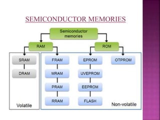
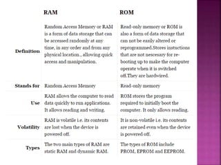
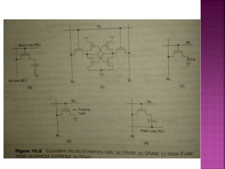

This document summarizes different types of semiconductor memories. DRAM uses a capacitor and transistor to store data as charge. SRAM uses a 6 transistor latch. Mask ROM is one-time programmable. EPROM and EEPROM can be reprogrammed using ultraviolet rays or electrical pulses. FRAM uses a ferroelectric capacitor. Memory cells are arranged in a grid and accessed using row and column decoders. The document then describes the operation of DRAM, SRAM, flash memory, and NAND flash memory cells.