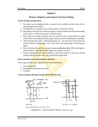
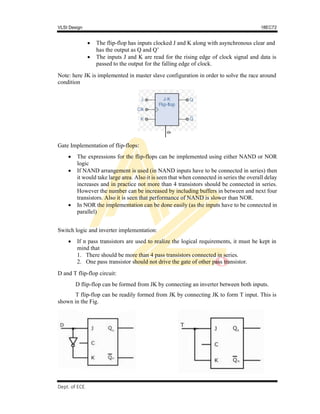
This document discusses system timing considerations and various memory cell designs used in VLSI systems. It describes:
1. A two-phase non-overlapping clock that is used throughout the system, with write operations occurring on the rising edge of the first clock phase and read operations on the rising edge of the second phase.
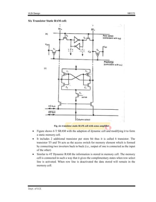
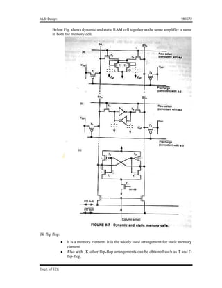
2. Common storage elements like DRAM, SRAM, and pseudo-static RAM cells, comparing their area, power dissipation, and volatility.
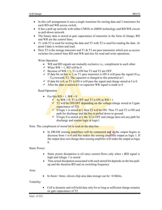
3. A 3T DRAM cell that stores a bit as charge on a transistor gate, using two access transistors for read and write operations.
![VLSI Design 18EC72
Dept. of ECE, SVIT 2017-18
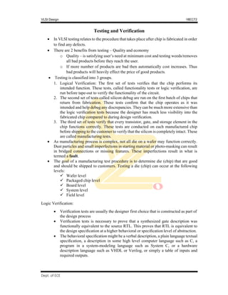
Area:
In 4mm× 4mm, silicon chip area data storage is about 12 Kbits.
Dissipation:
With the cell there is no static dissipation but switching energy while reading
and writing must be considered.
Volatility:
The data in Cm will be held only up-to 1msec or less. Thus periodic refreshing
must be provided
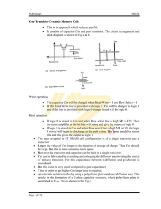
Pseudo-static RAM/register cell:
This is a memory cell which combines high storage capability of DRAM and ease of
use of SRAM
It can be used as SRAM as no external refreshing circuit is required and also used as
a DRAM having built-in refresh logic.
This is a static storage cell which will hold data indefinitely. This is achieved by
storing bit in 2 inverters with feedback. This feedback is used to refresh the data in
every clock cycle.
But care to be taken by not allowing read/write operation during internal refreshing.
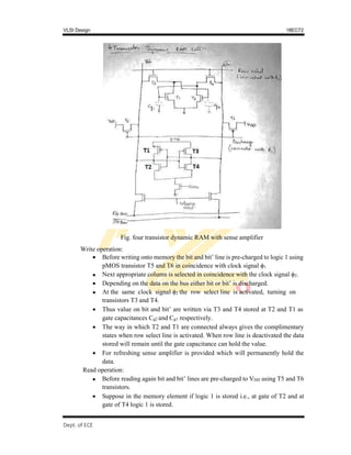
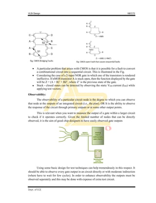
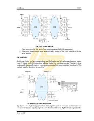
Circuit arrangement is as shown in the Fig.
Φ1 and ϕ2 are mutually exclusive clock signals, WR and RD signal coincides with ϕ1
signals
When ϕ1 is high and WR = 1, transistor T1 is ON and data is charged/stored on Cg
(gate capacitance) of inverter. This is write operation
When ϕ1 is high and RD = 1, transistor &the data stored at inverter stage is made
available at the output and also the compliment. Thus data is read at the output.
When Φ2 = 1, T3 is ON. The output is read and feedback i.e., refreshed (reading and
storing back the data). The gated feedback path from output of T2 is fed to the input
of T1.
The bit will be held as long as ϕ2 rescues and this time is less than decay time of stored
charged bit.
Note:
WR and RD must be mutually exclusive but both should coincide with ϕ1
During refreshing of memory cell i.e., at ϕ2 the cell must not be read. If an attempt is
made to read the cell data onto the bus, the charge sharing effect between bus and Cg
(input gate capacitance) may cause destruction of stored bit.
Other bus lines should be allowed to run through the cells so that register and memory
arrays can be easily configured.
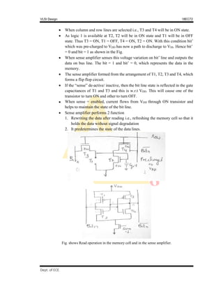
The Pseudo-static memory cell can also be implemented using transmission gate (TG).
This is seen the Fig. [replace nMOS transistors with TG]](https://image.slidesharecdn.com/vlsimodule5-220925142027-448692d5/85/VLSI-Module-5-pdf-4-320.jpg)
![VLSI Design 18EC72
, SVIT 2017-18
Dept. of ECE
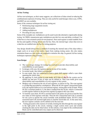
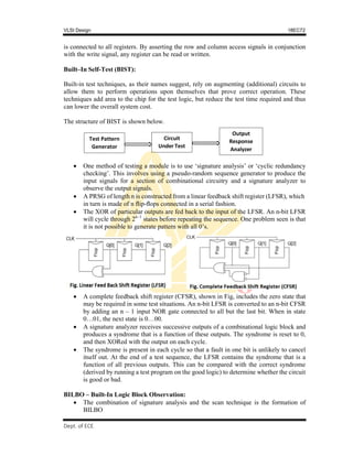
The 3-bit BIST register shown in Fig is a scannable, resettable register that also can
serve as a pattern generator and signature analyzer.
This structure can operate in different mode as shown in table below
C[1] C[0] Mode
0 0 Scan
0 1 Test
1 0 Reset
1 1 Normal
In the reset mode (10), all the flip-flops are synchronously initialized to 0. In normal
mode (11), the flip-flops behave normally with their D input and Q output. In scan
mode (00), the flip-flops are configured as a 3-bit shift register between SI and SO. In
test mode (01), the register behaves as a pseudo-random sequence generator or
signature analyzer.
In summary, BIST is performed by first resetting the syndrome in the output register.
Then both registers are placed in the test mode to produce the pseudo-random inputs
and calculate the syndrome. Finally, the syndrome is shifted out through the scan
chain.
Memory BIST:
On many chips, memories involves with majority of the transistors. A robust testing
methodology must be applied to provide reliable parts. In a typical MBIST scheme,
multiplexers are placed on the address, data, and control inputs for the memory to allow
direct access during test. During testing, a state machine uses these multiplexers to directly
write a checkerboard pattern of alternating 1s and 0s. The data is read back, checked, then
the inverse pattern is also applied and checked. ROM testing is even simpler: The contents
are read out to a signature analyzer to produce a syndrome.](https://image.slidesharecdn.com/vlsimodule5-220925142027-448692d5/85/VLSI-Module-5-pdf-20-320.jpg)


