SlideShare a Scribd company logo
1 of 38
M.Selvam. M.Sc., M.Phil., M.E., (Ph.D.,)
Assistant Professor
Department of Electronics and Communication Systems
Unit - V
M.Selvam, ECS, SKASC
Semiconductor Devices
• Conductor; Semiconductor
• Intrinsic Semiconductor
• Extrinsic semiconductor
– P type and N type Semiconductor
• PN junction diode; V-I characteristics; Applications
• Zener diode; V-I characteristics; Zener diode Applications
• Light Emitting Diode
M.Selvam, ECS, SKASC
Insulators:
– The valence band is full
– The conduction band is empty
– The Large forbidden energy gap ( > 6 eV )
• A large amount of energy is
required to shift electrons from
the valence band to the
conduction band.
• The electrical conductivity is
small or nil. So that it is called
as Insulator.
• Ex:
– Plastic, Rubber, Mica, Glass,
etc.
M.Selvam, ECS, SKASC
Conductors:
– Plenty of free electrons are available in the conduction band
– Overlapping valence and conduction bands
– No forbidden gap
• The free electrons in the
conduction band are
responsible for the conduction
of current .
• The materials which easily
allow the flow of electric
current through them are
called as conductors.
• Ex:
– Copper, Aluminium, etc.
M.Selvam, ECS, SKASC
Semiconductors:
At above 0K,
– The valence band is partially filled
– The conduction band is partially filled
– The narrow forbidden energy gap ( ~ 1 eV )
• A semiconductor is a material whose
electrical properties lie in between
the conductor and insulator.
• They require very small energy to
release an electron from their valance
band to conduction band.
• For Si, it is 1.1 eV and for Ge, it is 0.7
eV.
• Ex:
– Silicon (Si) and Germanium (Ge)..
M.Selvam, ECS, SKASC
Intrinsic Semiconductors:
• Extremely pure form of semiconductor is known as an Intrinsic
semiconductors.
• At absolute temperature (0K), the intrinsic semiconductors are acts as
insulators.
M.Selvam, ECS, SKASC
Intrinsic Semiconductors:
M.Selvam, ECS, SKASC
Intrinsic Semiconductors:
• Increase the temperature above 0K, the valence electrons gets sufficient
energy to jump across the small energy gap from the valence to the
conduction band.
• The positively charge holes are created in the valence band and the
conduction band having the free electrons.
• No. of free electros = No. of holes
• When an electric field is applied, the free electrons are move to the anode
terminal and holes are move to the cathode terminal.
M.Selvam, ECS, SKASC
Extrinsic Semiconductors
• To increase the conductivity of intrinsic semiconductor some suitable impurity or
doping agent is added (about 1:108) in intrinsic semiconductor.
• This final material is called extrinsic semiconductor.
• The process of adding impurity atoms to the intrinsic semiconductor is called
doping.
• Purpose of doping:
– To increase the no. of electrons
– To increase the no. of holes
• Pentavalent Impurity atom
– 5 Valence electrons
– It is know as donor atom – it donates one electron to the conduction band
– Ex:
• Phosphorous (P) – 15 (2+8+5)
• Arsenic (As) – 33 (2+8+18+5)
• Antimony (Sb) – 51 (2+8+18+18+5)
• Bismuth (Bi) – 83 (2+8+18+32+18+5)
M.Selvam, ECS, SKASC
Extrinsic Semiconductors
• Trivalent Impurity atom
– 3 Valence electrons
– It is know as accepter atom – it gains one electron
– Ex:
• Boron (B) – 5 (2+3)
• Aluminium (Al) – 13 (2+8+3)
• Gallium (Ga) – 31 (2+8+18+3)
• Indium (In) – 49 (2+8+18+18+3)
• Based on the dopant, the Extrinsic semiconductor can be classified,
– N-Type Semiconductor
– P-Type Semiconductor
M.Selvam, ECS, SKASC
N-Type Semiconductors
• The pure silicon is doped with a group-5 element such as
phosphorus, antimony, arsenic. These materials have atoms
with five valence electrons (pentavalent atoms).
• Four of these electrons will form covalent bonds with
neighboring silicon atoms and the fifth electron is not part of a
covalent bond, and is therefore a free electron.
• Every impurity atom will produce a free electron in the
conduction band. These electrons will drift to produce an
electrical current.
• N-type semiconductor is a much better conductor than the
intrinsic pure silicon material.
M.Selvam, ECS, SKASC
N-Type Semiconductors
M.Selvam, ECS, SKASC
P-Type Semiconductors
• The pure silicon is doped with a group-3 element such as Boron,
Aluminium, Gallium. These materials have atoms with three
valence electrons (tritavalent atoms).
• Three of these electrons will form covalent bonds with
neighboring silicon atoms and a hole is created in the valence
band which will drift to conduct electric current if a potential is
applied to the material.
• P-type semiconductor is a much better conductor than the
intrinsic pure silicon material.
M.Selvam, ECS, SKASC
P-Type Semiconductors
M.Selvam, ECS, SKASC
• The N-type material has mobile negative majority carriers (electrons) with
immobile donor ions (+ve). The P-type material has mobile positive majority
carriers (holes) with immobile acceptor ions (-ve).
• Near the junction, electrons from the n-type start to diffuse into the p-type.
Similarly, holes in the p-type side start to diffuse across into the n-type side.
• Near the interface, they leaves positively charged ions in N side and
negatively charged ions in P side. The majority charge carriers have been
depleted in this region, it is known as the depletion region or space charge
region.
M.Selvam, ECS, SKASC
• The fixed immobile ions "built-up" an electric field right at the junction
between the n-type and p-type material. This opposes further diffusion of
carriers. Therefore, the net flow of electrons across the junction is zero and
the net flow of holes across the junction is also zero.
• This separation of charges at the PN junction constitutes a potential
barrier. This potential barrier must be overcome by an external voltage
to make the junction conduct.
• This region becomes nonconductive. It is like an insulator separated by the
conductive P and N type materials. Therefore the PN junction have a
capacitance called junction capacitance.
The barrier potential of
Silicon lattice is 0.7 Volt and
Germanium lattice is 0.3 Volt
M.Selvam, ECS, SKASC
• The diode is two terminal semiconductor device which is actually
manufactured as a single piece of PN type semiconductor material.
• The diode is a unidirectional device. Electron current flows in one direction.
• The anode of diode symbol corresponds to P-type semiconductor. The
cathode corresponds to the N-type semiconductor.
M.Selvam, ECS, SKASC
• The VI characteristics is a graph between the voltage applied across the
terminals of device and the current flows through it.
• The VI graph can be divided into two parts namely forward characteristics
and reverse characteristics.
• Forward characteristics
• It is a voltage vs current graph when the device is connected in
forward bias.
• Reverse characteristics
• It is a voltage vs current graph when the device is connected in
reverse bias.
Forward Characteristics
• Forward bias of PN junction diode: The positive terminal of voltage source is
connected to the anode (+) of diode and negative terminal to the cathode
(-).
M.Selvam, ECS, SKASC
• In forward bias, the holes in P-type are repelled by the +ve terminal of
voltage source and electrons are repelled by –ve terminal of voltage source.
• Width of the barrier or depletion layer is reduced and resistance of junction
also decreased.
M.Selvam, ECS, SKASC
• If this external voltage becomes greater than the value of the potential
barrier, approx. 0.7 volts for silicon and 0.3 volts for germanium (Knee
Voltage), the potential barriers opposition will be overcome and current will
start to flow.
M.Selvam, ECS, SKASC
Reverse Characteristics
• Reverse bias of PN junction diode: The positive terminal of voltage source
connected to the cathode of diode and negative terminal to the anode.
M.Selvam, ECS, SKASC
• In reverse bias, holes in P-type are attracted by the negative terminal of
voltage source and electrons in N-type are attracted by the positive terminal
of voltage source.
• Therefore, there is no electron-hole combination and no current flow.
• Width of the barrier or depletion layer is increased and junction offers high
resistance.
• The value of small current (in uA) due to reverse saturation current or
leakage current (because of minority carriers) .
M.Selvam, ECS, SKASC
• When we apply a high reverse voltage across the diode, free electrons
(minority carriers) will gain acceleration and it will start moving across the
junction with high velocity. This results in collision with other neighboring
atoms. These collisions in high velocity will generate further free electrons
(avalanche multiplication). These electrons will start drifting and electron-
hole pair recombination occurs across the junction. This results in net
current that rapidly increases. It may damage the junction. The
corresponding applied voltage is referred to as the breakdown voltage.
Therefore, care should be taken that reverse voltage across a PN junction is
always less than the breakdown voltage.
Applications:
• Used as a rectifier – converts AC into DC.
• Used as signal diode in communication circuits for demodulation of signals.
• Used in logical circuit design.
M.Selvam, ECS, SKASC
• A Zener Diode is a special kind of diode which permits current to flow in the
forward direction as normal diode, It also permits the current to flow in the
reverse direction when the voltage is above a certain value known as the
breakdown voltage.
• Breakdown voltage is also known as Zener voltage.
• Zener diode is highly doped p-n junction diode.
• Zener Diodes are normally used only in the reverse bias direction.
Conventional diodes or rectifiers never operate in the breakdown region, but
the Zener diode can safely be operated at this point.
M.Selvam, ECS, SKASC
Working of Zener diode
The V-I Characteristics of a Zener Diode can be divided into two parts
(i) Forward Characteristics
(ii) Reverse Characteristics
• The forward characteristics of Zener diode is similar to that of normal PN
junction diode.
M.Selvam, ECS, SKASC
• In reverse characteristics, the reverse voltage applied to the Zener diode
increases, it reaches the breakdown voltage at which Zener current
increases to a large value. In the breakdown region, further increase in
reverse voltage will not increase the voltage across the Zener diode, it only
increases the current. Thus, a constant voltage called Zener voltage (Vz) is
maintained across the Zener diode when the supply voltage changes.
• Hence, Zener diode acts as a voltage regulator in reverse biased condition.
M.Selvam, ECS, SKASC
I. Zener diode is used as a voltage regulator.
II. Zener diode is used as a peak clipper in wave shaping circuits.
III. Zener diode is used as a fixed reference voltage in transistor
biasing circuits.
IV. Zener diode is used for meter protection against damage from
accidental application of excessive voltages.
Light Emitting Diode
• The Light emitting diode is a two-lead semiconductor light source. In 1962,
Nick Holonyak has come up with an idea of light emitting diode, and he
was working for the general electric company.
• The LED is a special type of diode and they have similar electrical
characteristics of a PN junction diode.
• The LED allows the flow of current in the forward direction and blocks the
current in the reverse direction
• It is a specially doped diode and made up of a special type of
semiconductors. When the light emits in the forward biased, then it
is called as a light emitting diode.
M.Selvam, ECS, SKASC
Light Emitting Diode
M.Selvam, ECS, SKASC
LED Basic Operation
• The holes are present in the valance band and the free electrons are in the
conduction band.
• When a p-n junction is forward biased, the electron from n-type
semiconductor material cross the p-n junction and combine with the holes
in the p-type semiconductor material. Thus with respect to the holes, the
free electrons are at higher energy level.
M.Selvam, ECS, SKASC
Light Emitting Diode
M.Selvam, ECS, SKASC
• When a free electron recombines with hole, the energy level related with
it changes from higher value to the lower value and it falls from the
conduction band to the valance band.
• There is an energy release due to the electron travel. In normal diodes,
this energy released is in the form of heat. But in LED the energy release in
the form of photons which emit the light energy. The entire process is
called electroluminescence and the diodes are called the light emitting
diode.
• In LED, energy released in the form of light depends on the forbidden
energy gap. One can determine the wavelength of the light emitted.
Hence the color of the light and also whether the light is visible or not can
be determined from wavelength. The color and wavelength of the emitted
light can be controlled by doping with various impurities.
Types of Light Emitting Diodes
There are different types of light emitting diodes present and some of them
are mentioned below.
• Gallium Arsenide (GaAs) – infra-red
• Gallium Arsenide Phosphide (GaAsP) – red to infra-red, orange
• Aluminium Gallium Arsenide Phosphide (AlGaAsP) – high-brightness red,
orange-red, orange, and yellow
• Gallium Phosphide (GaP) – red, yellow and green
• Aluminium Gallium Phosphide (AlGaP) – green
• Gallium Nitride (GaN) – green, emerald green
• Gallium Indium Nitride (GaInN) – near ultraviolet, bluish-green and blue
• Silicon Carbide (SiC) – blue as a substrate
• Zinc Selenide (ZnSe) – blue
• Aluminium Gallium Nitride (AlGaN) – ultraviolet
M.Selvam, ECS, SKASC
I-V Characteristics of LED
• There are different types of light emitting diodes are available in the
market and there are different LED characteristics which include the color
light, or wavelength radiation, light intensity.
• The important characteristic of the LED is color. In the starting use of LED,
there is the only red color. As the use of LED is increased with the help of
the semiconductor process and doing the research on the new metals for
LED, the different colors were formed.
M.Selvam, ECS, SKASC
I-V Characteristics of LED
The following graph shows the approximate curves between the forward voltage and
the current. Each curve in the graph indicates the different color. The table shows the
summary of the LED characteristics.
M.Selvam, ECS, SKASC
Applications of Light Emitting Diodes
There are many applications of the LED and some of them are
explained below.
• LED is used as a bulb in the homes and industries
• The light emitting diodes are used in the motorcycles and cars
• These are used in the mobile phones to display the message
• At the traffic light signals led’s are used
M.Selvam, ECS, SKASC
THANK
YOU

More Related Content

Similar to Unit-5.pptx

[FULL ANIMATED(Download to view)] Unbiased diode, Forward biased , reverse bi...
[FULL ANIMATED(Download to view)] Unbiased diode, Forward biased , reverse bi...[FULL ANIMATED(Download to view)] Unbiased diode, Forward biased , reverse bi...
[FULL ANIMATED(Download to view)] Unbiased diode, Forward biased , reverse bi...Pratik Nakrani
 
Semiconductor optoelectronic materials
Semiconductor optoelectronic materialsSemiconductor optoelectronic materials
Semiconductor optoelectronic materialskrishslide
 
Topic 3 pn_junction_and_diode
Topic 3 pn_junction_and_diodeTopic 3 pn_junction_and_diode
Topic 3 pn_junction_and_diodeGabriel O'Brien
 
EST 130, Semiconductors
EST 130, SemiconductorsEST 130, Semiconductors
EST 130, SemiconductorsCKSunith1
 
Analog electrons introduction
Analog electrons introductionAnalog electrons introduction
Analog electrons introductionP.sudharsan Rao
 
B.tech sem i engineering physics u ii chapter 1-band theory of solid
B.tech sem i engineering physics u ii chapter 1-band theory of solidB.tech sem i engineering physics u ii chapter 1-band theory of solid
B.tech sem i engineering physics u ii chapter 1-band theory of solidRai University
 
Conductor semiconductor insulator
Conductor semiconductor insulatorConductor semiconductor insulator
Conductor semiconductor insulatorravikumar s
 
BEEIE UNIT IV PPT.ppt
BEEIE UNIT IV PPT.pptBEEIE UNIT IV PPT.ppt
BEEIE UNIT IV PPT.pptDEEBIKAR2
 
Material engineering and its applications.
Material engineering and its applications.Material engineering and its applications.
Material engineering and its applications.Omkar Rane
 
SEMICONDUCTOR (project)
SEMICONDUCTOR (project)SEMICONDUCTOR (project)
SEMICONDUCTOR (project)SUDHA BHUJEL
 
Introduction to Semiconductors.ppt
Introduction to Semiconductors.pptIntroduction to Semiconductors.ppt
Introduction to Semiconductors.pptChristianAceSolidum
 
Introduction_Semi_Materials-6-09-10.ppt
Introduction_Semi_Materials-6-09-10.pptIntroduction_Semi_Materials-6-09-10.ppt
Introduction_Semi_Materials-6-09-10.pptAnna336806
 
Introduction_Semi_Materials-6-09-10.ppt
Introduction_Semi_Materials-6-09-10.pptIntroduction_Semi_Materials-6-09-10.ppt
Introduction_Semi_Materials-6-09-10.pptRyanAnderson41811
 
UNIT 1- Semiconductor diodes (3).pptx
UNIT 1- Semiconductor diodes (3).pptxUNIT 1- Semiconductor diodes (3).pptx
UNIT 1- Semiconductor diodes (3).pptxnakkabava24
 
Basic electronics
Basic electronicsBasic electronics
Basic electronicsmorin moli
 

Similar to Unit-5.pptx (20)

BEEE.pptx
BEEE.pptxBEEE.pptx
BEEE.pptx
 
[FULL ANIMATED(Download to view)] Unbiased diode, Forward biased , reverse bi...
[FULL ANIMATED(Download to view)] Unbiased diode, Forward biased , reverse bi...[FULL ANIMATED(Download to view)] Unbiased diode, Forward biased , reverse bi...
[FULL ANIMATED(Download to view)] Unbiased diode, Forward biased , reverse bi...
 
Semiconductor optoelectronic materials
Semiconductor optoelectronic materialsSemiconductor optoelectronic materials
Semiconductor optoelectronic materials
 
BEEME UNIT IV.ppt
BEEME UNIT IV.pptBEEME UNIT IV.ppt
BEEME UNIT IV.ppt
 
Semiconductors
SemiconductorsSemiconductors
Semiconductors
 
Topic 3 pn_junction_and_diode
Topic 3 pn_junction_and_diodeTopic 3 pn_junction_and_diode
Topic 3 pn_junction_and_diode
 
EST 130, Semiconductors
EST 130, SemiconductorsEST 130, Semiconductors
EST 130, Semiconductors
 
Analog electrons introduction
Analog electrons introductionAnalog electrons introduction
Analog electrons introduction
 
B.tech sem i engineering physics u ii chapter 1-band theory of solid
B.tech sem i engineering physics u ii chapter 1-band theory of solidB.tech sem i engineering physics u ii chapter 1-band theory of solid
B.tech sem i engineering physics u ii chapter 1-band theory of solid
 
Conductor semiconductor insulator
Conductor semiconductor insulatorConductor semiconductor insulator
Conductor semiconductor insulator
 
BEEIE UNIT IV PPT.ppt
BEEIE UNIT IV PPT.pptBEEIE UNIT IV PPT.ppt
BEEIE UNIT IV PPT.ppt
 
Material engineering and its applications.
Material engineering and its applications.Material engineering and its applications.
Material engineering and its applications.
 
Theory of solids
Theory of solidsTheory of solids
Theory of solids
 
SEMICONDUCTOR (project)
SEMICONDUCTOR (project)SEMICONDUCTOR (project)
SEMICONDUCTOR (project)
 
Introduction to Semiconductors.ppt
Introduction to Semiconductors.pptIntroduction to Semiconductors.ppt
Introduction to Semiconductors.ppt
 
Introduction_Semi_Materials-6-09-10.ppt
Introduction_Semi_Materials-6-09-10.pptIntroduction_Semi_Materials-6-09-10.ppt
Introduction_Semi_Materials-6-09-10.ppt
 
Introduction_Semi_Materials-6-09-10.ppt
Introduction_Semi_Materials-6-09-10.pptIntroduction_Semi_Materials-6-09-10.ppt
Introduction_Semi_Materials-6-09-10.ppt
 
UNIT 1- Semiconductor diodes (3).pptx
UNIT 1- Semiconductor diodes (3).pptxUNIT 1- Semiconductor diodes (3).pptx
UNIT 1- Semiconductor diodes (3).pptx
 
Basic electronics
Basic electronicsBasic electronics
Basic electronics
 
Basic electronics
Basic electronicsBasic electronics
Basic electronics
 

Recently uploaded

APPLICATIONS-AC/DC DRIVES-OPERATING CHARACTERISTICS
APPLICATIONS-AC/DC DRIVES-OPERATING CHARACTERISTICSAPPLICATIONS-AC/DC DRIVES-OPERATING CHARACTERISTICS
APPLICATIONS-AC/DC DRIVES-OPERATING CHARACTERISTICSKurinjimalarL3
 
Study on Air-Water & Water-Water Heat Exchange in a Finned Tube Exchanger
Study on Air-Water & Water-Water Heat Exchange in a Finned Tube ExchangerStudy on Air-Water & Water-Water Heat Exchange in a Finned Tube Exchanger
Study on Air-Water & Water-Water Heat Exchange in a Finned Tube ExchangerAnamika Sarkar
 
INFLUENCE OF NANOSILICA ON THE PROPERTIES OF CONCRETE
INFLUENCE OF NANOSILICA ON THE PROPERTIES OF CONCRETEINFLUENCE OF NANOSILICA ON THE PROPERTIES OF CONCRETE
INFLUENCE OF NANOSILICA ON THE PROPERTIES OF CONCRETEroselinkalist12
 
main PPT.pptx of girls hostel security using rfid
main PPT.pptx of girls hostel security using rfidmain PPT.pptx of girls hostel security using rfid
main PPT.pptx of girls hostel security using rfidNikhilNagaraju
 
HARMONY IN THE NATURE AND EXISTENCE - Unit-IV
HARMONY IN THE NATURE AND EXISTENCE - Unit-IVHARMONY IN THE NATURE AND EXISTENCE - Unit-IV
HARMONY IN THE NATURE AND EXISTENCE - Unit-IVRajaP95
 
OSVC_Meta-Data based Simulation Automation to overcome Verification Challenge...
OSVC_Meta-Data based Simulation Automation to overcome Verification Challenge...OSVC_Meta-Data based Simulation Automation to overcome Verification Challenge...
OSVC_Meta-Data based Simulation Automation to overcome Verification Challenge...Soham Mondal
 
Current Transformer Drawing and GTP for MSETCL
Current Transformer Drawing and GTP for MSETCLCurrent Transformer Drawing and GTP for MSETCL
Current Transformer Drawing and GTP for MSETCLDeelipZope
 
Sachpazis Costas: Geotechnical Engineering: A student's Perspective Introduction
Sachpazis Costas: Geotechnical Engineering: A student's Perspective IntroductionSachpazis Costas: Geotechnical Engineering: A student's Perspective Introduction
Sachpazis Costas: Geotechnical Engineering: A student's Perspective IntroductionDr.Costas Sachpazis
 
Introduction to Microprocesso programming and interfacing.pptx
Introduction to Microprocesso programming and interfacing.pptxIntroduction to Microprocesso programming and interfacing.pptx
Introduction to Microprocesso programming and interfacing.pptxvipinkmenon1
 
HARMONY IN THE HUMAN BEING - Unit-II UHV-2
HARMONY IN THE HUMAN BEING - Unit-II UHV-2HARMONY IN THE HUMAN BEING - Unit-II UHV-2
HARMONY IN THE HUMAN BEING - Unit-II UHV-2RajaP95
 
chaitra-1.pptx fake news detection using machine learning
chaitra-1.pptx  fake news detection using machine learningchaitra-1.pptx  fake news detection using machine learning
chaitra-1.pptx fake news detection using machine learningmisbanausheenparvam
 
What are the advantages and disadvantages of membrane structures.pptx
What are the advantages and disadvantages of membrane structures.pptxWhat are the advantages and disadvantages of membrane structures.pptx
What are the advantages and disadvantages of membrane structures.pptxwendy cai
 
CCS355 Neural Network & Deep Learning UNIT III notes and Question bank .pdf
CCS355 Neural Network & Deep Learning UNIT III notes and Question bank .pdfCCS355 Neural Network & Deep Learning UNIT III notes and Question bank .pdf
CCS355 Neural Network & Deep Learning UNIT III notes and Question bank .pdfAsst.prof M.Gokilavani
 
Internship report on mechanical engineering
Internship report on mechanical engineeringInternship report on mechanical engineering
Internship report on mechanical engineeringmalavadedarshan25
 
IVE Industry Focused Event - Defence Sector 2024
IVE Industry Focused Event - Defence Sector 2024IVE Industry Focused Event - Defence Sector 2024
IVE Industry Focused Event - Defence Sector 2024Mark Billinghurst
 
Electronically Controlled suspensions system .pdf
Electronically Controlled suspensions system .pdfElectronically Controlled suspensions system .pdf
Electronically Controlled suspensions system .pdfme23b1001
 
Biology for Computer Engineers Course Handout.pptx
Biology for Computer Engineers Course Handout.pptxBiology for Computer Engineers Course Handout.pptx
Biology for Computer Engineers Course Handout.pptxDeepakSakkari2
 
VICTOR MAESTRE RAMIREZ - Planetary Defender on NASA's Double Asteroid Redirec...
VICTOR MAESTRE RAMIREZ - Planetary Defender on NASA's Double Asteroid Redirec...VICTOR MAESTRE RAMIREZ - Planetary Defender on NASA's Double Asteroid Redirec...
VICTOR MAESTRE RAMIREZ - Planetary Defender on NASA's Double Asteroid Redirec...VICTOR MAESTRE RAMIREZ
 

Recently uploaded (20)

APPLICATIONS-AC/DC DRIVES-OPERATING CHARACTERISTICS
APPLICATIONS-AC/DC DRIVES-OPERATING CHARACTERISTICSAPPLICATIONS-AC/DC DRIVES-OPERATING CHARACTERISTICS
APPLICATIONS-AC/DC DRIVES-OPERATING CHARACTERISTICS
 
young call girls in Green Park🔝 9953056974 🔝 escort Service
young call girls in Green Park🔝 9953056974 🔝 escort Serviceyoung call girls in Green Park🔝 9953056974 🔝 escort Service
young call girls in Green Park🔝 9953056974 🔝 escort Service
 
Study on Air-Water & Water-Water Heat Exchange in a Finned Tube Exchanger
Study on Air-Water & Water-Water Heat Exchange in a Finned Tube ExchangerStudy on Air-Water & Water-Water Heat Exchange in a Finned Tube Exchanger
Study on Air-Water & Water-Water Heat Exchange in a Finned Tube Exchanger
 
INFLUENCE OF NANOSILICA ON THE PROPERTIES OF CONCRETE
INFLUENCE OF NANOSILICA ON THE PROPERTIES OF CONCRETEINFLUENCE OF NANOSILICA ON THE PROPERTIES OF CONCRETE
INFLUENCE OF NANOSILICA ON THE PROPERTIES OF CONCRETE
 
main PPT.pptx of girls hostel security using rfid
main PPT.pptx of girls hostel security using rfidmain PPT.pptx of girls hostel security using rfid
main PPT.pptx of girls hostel security using rfid
 
HARMONY IN THE NATURE AND EXISTENCE - Unit-IV
HARMONY IN THE NATURE AND EXISTENCE - Unit-IVHARMONY IN THE NATURE AND EXISTENCE - Unit-IV
HARMONY IN THE NATURE AND EXISTENCE - Unit-IV
 
OSVC_Meta-Data based Simulation Automation to overcome Verification Challenge...
OSVC_Meta-Data based Simulation Automation to overcome Verification Challenge...OSVC_Meta-Data based Simulation Automation to overcome Verification Challenge...
OSVC_Meta-Data based Simulation Automation to overcome Verification Challenge...
 
Current Transformer Drawing and GTP for MSETCL
Current Transformer Drawing and GTP for MSETCLCurrent Transformer Drawing and GTP for MSETCL
Current Transformer Drawing and GTP for MSETCL
 
Sachpazis Costas: Geotechnical Engineering: A student's Perspective Introduction
Sachpazis Costas: Geotechnical Engineering: A student's Perspective IntroductionSachpazis Costas: Geotechnical Engineering: A student's Perspective Introduction
Sachpazis Costas: Geotechnical Engineering: A student's Perspective Introduction
 
Introduction to Microprocesso programming and interfacing.pptx
Introduction to Microprocesso programming and interfacing.pptxIntroduction to Microprocesso programming and interfacing.pptx
Introduction to Microprocesso programming and interfacing.pptx
 
HARMONY IN THE HUMAN BEING - Unit-II UHV-2
HARMONY IN THE HUMAN BEING - Unit-II UHV-2HARMONY IN THE HUMAN BEING - Unit-II UHV-2
HARMONY IN THE HUMAN BEING - Unit-II UHV-2
 
chaitra-1.pptx fake news detection using machine learning
chaitra-1.pptx  fake news detection using machine learningchaitra-1.pptx  fake news detection using machine learning
chaitra-1.pptx fake news detection using machine learning
 
What are the advantages and disadvantages of membrane structures.pptx
What are the advantages and disadvantages of membrane structures.pptxWhat are the advantages and disadvantages of membrane structures.pptx
What are the advantages and disadvantages of membrane structures.pptx
 
POWER SYSTEMS-1 Complete notes examples
POWER SYSTEMS-1 Complete notes  examplesPOWER SYSTEMS-1 Complete notes  examples
POWER SYSTEMS-1 Complete notes examples
 
CCS355 Neural Network & Deep Learning UNIT III notes and Question bank .pdf
CCS355 Neural Network & Deep Learning UNIT III notes and Question bank .pdfCCS355 Neural Network & Deep Learning UNIT III notes and Question bank .pdf
CCS355 Neural Network & Deep Learning UNIT III notes and Question bank .pdf
 
Internship report on mechanical engineering
Internship report on mechanical engineeringInternship report on mechanical engineering
Internship report on mechanical engineering
 
IVE Industry Focused Event - Defence Sector 2024
IVE Industry Focused Event - Defence Sector 2024IVE Industry Focused Event - Defence Sector 2024
IVE Industry Focused Event - Defence Sector 2024
 
Electronically Controlled suspensions system .pdf
Electronically Controlled suspensions system .pdfElectronically Controlled suspensions system .pdf
Electronically Controlled suspensions system .pdf
 
Biology for Computer Engineers Course Handout.pptx
Biology for Computer Engineers Course Handout.pptxBiology for Computer Engineers Course Handout.pptx
Biology for Computer Engineers Course Handout.pptx
 
VICTOR MAESTRE RAMIREZ - Planetary Defender on NASA's Double Asteroid Redirec...
VICTOR MAESTRE RAMIREZ - Planetary Defender on NASA's Double Asteroid Redirec...VICTOR MAESTRE RAMIREZ - Planetary Defender on NASA's Double Asteroid Redirec...
VICTOR MAESTRE RAMIREZ - Planetary Defender on NASA's Double Asteroid Redirec...
 

Unit-5.pptx

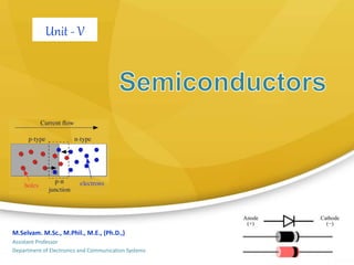
  • 1. M.Selvam. M.Sc., M.Phil., M.E., (Ph.D.,) Assistant Professor Department of Electronics and Communication Systems Unit - V
  • 2. M.Selvam, ECS, SKASC Semiconductor Devices • Conductor; Semiconductor • Intrinsic Semiconductor • Extrinsic semiconductor – P type and N type Semiconductor • PN junction diode; V-I characteristics; Applications • Zener diode; V-I characteristics; Zener diode Applications • Light Emitting Diode
  • 3. M.Selvam, ECS, SKASC Insulators: – The valence band is full – The conduction band is empty – The Large forbidden energy gap ( > 6 eV ) • A large amount of energy is required to shift electrons from the valence band to the conduction band. • The electrical conductivity is small or nil. So that it is called as Insulator. • Ex: – Plastic, Rubber, Mica, Glass, etc.
  • 4. M.Selvam, ECS, SKASC Conductors: – Plenty of free electrons are available in the conduction band – Overlapping valence and conduction bands – No forbidden gap • The free electrons in the conduction band are responsible for the conduction of current . • The materials which easily allow the flow of electric current through them are called as conductors. • Ex: – Copper, Aluminium, etc.
  • 5. M.Selvam, ECS, SKASC Semiconductors: At above 0K, – The valence band is partially filled – The conduction band is partially filled – The narrow forbidden energy gap ( ~ 1 eV ) • A semiconductor is a material whose electrical properties lie in between the conductor and insulator. • They require very small energy to release an electron from their valance band to conduction band. • For Si, it is 1.1 eV and for Ge, it is 0.7 eV. • Ex: – Silicon (Si) and Germanium (Ge)..
  • 6. M.Selvam, ECS, SKASC Intrinsic Semiconductors: • Extremely pure form of semiconductor is known as an Intrinsic semiconductors. • At absolute temperature (0K), the intrinsic semiconductors are acts as insulators.
  • 8. M.Selvam, ECS, SKASC Intrinsic Semiconductors: • Increase the temperature above 0K, the valence electrons gets sufficient energy to jump across the small energy gap from the valence to the conduction band. • The positively charge holes are created in the valence band and the conduction band having the free electrons. • No. of free electros = No. of holes • When an electric field is applied, the free electrons are move to the anode terminal and holes are move to the cathode terminal.
  • 9. M.Selvam, ECS, SKASC Extrinsic Semiconductors • To increase the conductivity of intrinsic semiconductor some suitable impurity or doping agent is added (about 1:108) in intrinsic semiconductor. • This final material is called extrinsic semiconductor. • The process of adding impurity atoms to the intrinsic semiconductor is called doping. • Purpose of doping: – To increase the no. of electrons – To increase the no. of holes • Pentavalent Impurity atom – 5 Valence electrons – It is know as donor atom – it donates one electron to the conduction band – Ex: • Phosphorous (P) – 15 (2+8+5) • Arsenic (As) – 33 (2+8+18+5) • Antimony (Sb) – 51 (2+8+18+18+5) • Bismuth (Bi) – 83 (2+8+18+32+18+5)
  • 10. M.Selvam, ECS, SKASC Extrinsic Semiconductors • Trivalent Impurity atom – 3 Valence electrons – It is know as accepter atom – it gains one electron – Ex: • Boron (B) – 5 (2+3) • Aluminium (Al) – 13 (2+8+3) • Gallium (Ga) – 31 (2+8+18+3) • Indium (In) – 49 (2+8+18+18+3) • Based on the dopant, the Extrinsic semiconductor can be classified, – N-Type Semiconductor – P-Type Semiconductor
  • 11. M.Selvam, ECS, SKASC N-Type Semiconductors • The pure silicon is doped with a group-5 element such as phosphorus, antimony, arsenic. These materials have atoms with five valence electrons (pentavalent atoms). • Four of these electrons will form covalent bonds with neighboring silicon atoms and the fifth electron is not part of a covalent bond, and is therefore a free electron. • Every impurity atom will produce a free electron in the conduction band. These electrons will drift to produce an electrical current. • N-type semiconductor is a much better conductor than the intrinsic pure silicon material.
  • 12. M.Selvam, ECS, SKASC N-Type Semiconductors
  • 13. M.Selvam, ECS, SKASC P-Type Semiconductors • The pure silicon is doped with a group-3 element such as Boron, Aluminium, Gallium. These materials have atoms with three valence electrons (tritavalent atoms). • Three of these electrons will form covalent bonds with neighboring silicon atoms and a hole is created in the valence band which will drift to conduct electric current if a potential is applied to the material. • P-type semiconductor is a much better conductor than the intrinsic pure silicon material.
  • 14. M.Selvam, ECS, SKASC P-Type Semiconductors
  • 17. M.Selvam, ECS, SKASC • The N-type material has mobile negative majority carriers (electrons) with immobile donor ions (+ve). The P-type material has mobile positive majority carriers (holes) with immobile acceptor ions (-ve). • Near the junction, electrons from the n-type start to diffuse into the p-type. Similarly, holes in the p-type side start to diffuse across into the n-type side. • Near the interface, they leaves positively charged ions in N side and negatively charged ions in P side. The majority charge carriers have been depleted in this region, it is known as the depletion region or space charge region.
  • 18. M.Selvam, ECS, SKASC • The fixed immobile ions "built-up" an electric field right at the junction between the n-type and p-type material. This opposes further diffusion of carriers. Therefore, the net flow of electrons across the junction is zero and the net flow of holes across the junction is also zero. • This separation of charges at the PN junction constitutes a potential barrier. This potential barrier must be overcome by an external voltage to make the junction conduct. • This region becomes nonconductive. It is like an insulator separated by the conductive P and N type materials. Therefore the PN junction have a capacitance called junction capacitance. The barrier potential of Silicon lattice is 0.7 Volt and Germanium lattice is 0.3 Volt
  • 19. M.Selvam, ECS, SKASC • The diode is two terminal semiconductor device which is actually manufactured as a single piece of PN type semiconductor material. • The diode is a unidirectional device. Electron current flows in one direction. • The anode of diode symbol corresponds to P-type semiconductor. The cathode corresponds to the N-type semiconductor.
  • 20. M.Selvam, ECS, SKASC • The VI characteristics is a graph between the voltage applied across the terminals of device and the current flows through it. • The VI graph can be divided into two parts namely forward characteristics and reverse characteristics. • Forward characteristics • It is a voltage vs current graph when the device is connected in forward bias. • Reverse characteristics • It is a voltage vs current graph when the device is connected in reverse bias. Forward Characteristics • Forward bias of PN junction diode: The positive terminal of voltage source is connected to the anode (+) of diode and negative terminal to the cathode (-).
  • 21. M.Selvam, ECS, SKASC • In forward bias, the holes in P-type are repelled by the +ve terminal of voltage source and electrons are repelled by –ve terminal of voltage source. • Width of the barrier or depletion layer is reduced and resistance of junction also decreased.
  • 22. M.Selvam, ECS, SKASC • If this external voltage becomes greater than the value of the potential barrier, approx. 0.7 volts for silicon and 0.3 volts for germanium (Knee Voltage), the potential barriers opposition will be overcome and current will start to flow.
  • 23. M.Selvam, ECS, SKASC Reverse Characteristics • Reverse bias of PN junction diode: The positive terminal of voltage source connected to the cathode of diode and negative terminal to the anode.
  • 24. M.Selvam, ECS, SKASC • In reverse bias, holes in P-type are attracted by the negative terminal of voltage source and electrons in N-type are attracted by the positive terminal of voltage source. • Therefore, there is no electron-hole combination and no current flow. • Width of the barrier or depletion layer is increased and junction offers high resistance. • The value of small current (in uA) due to reverse saturation current or leakage current (because of minority carriers) .
  • 25. M.Selvam, ECS, SKASC • When we apply a high reverse voltage across the diode, free electrons (minority carriers) will gain acceleration and it will start moving across the junction with high velocity. This results in collision with other neighboring atoms. These collisions in high velocity will generate further free electrons (avalanche multiplication). These electrons will start drifting and electron- hole pair recombination occurs across the junction. This results in net current that rapidly increases. It may damage the junction. The corresponding applied voltage is referred to as the breakdown voltage. Therefore, care should be taken that reverse voltage across a PN junction is always less than the breakdown voltage. Applications: • Used as a rectifier – converts AC into DC. • Used as signal diode in communication circuits for demodulation of signals. • Used in logical circuit design.
  • 26. M.Selvam, ECS, SKASC • A Zener Diode is a special kind of diode which permits current to flow in the forward direction as normal diode, It also permits the current to flow in the reverse direction when the voltage is above a certain value known as the breakdown voltage. • Breakdown voltage is also known as Zener voltage. • Zener diode is highly doped p-n junction diode. • Zener Diodes are normally used only in the reverse bias direction. Conventional diodes or rectifiers never operate in the breakdown region, but the Zener diode can safely be operated at this point.
  • 27. M.Selvam, ECS, SKASC Working of Zener diode The V-I Characteristics of a Zener Diode can be divided into two parts (i) Forward Characteristics (ii) Reverse Characteristics • The forward characteristics of Zener diode is similar to that of normal PN junction diode.
  • 28. M.Selvam, ECS, SKASC • In reverse characteristics, the reverse voltage applied to the Zener diode increases, it reaches the breakdown voltage at which Zener current increases to a large value. In the breakdown region, further increase in reverse voltage will not increase the voltage across the Zener diode, it only increases the current. Thus, a constant voltage called Zener voltage (Vz) is maintained across the Zener diode when the supply voltage changes. • Hence, Zener diode acts as a voltage regulator in reverse biased condition.
  • 29. M.Selvam, ECS, SKASC I. Zener diode is used as a voltage regulator. II. Zener diode is used as a peak clipper in wave shaping circuits. III. Zener diode is used as a fixed reference voltage in transistor biasing circuits. IV. Zener diode is used for meter protection against damage from accidental application of excessive voltages.
  • 30. Light Emitting Diode • The Light emitting diode is a two-lead semiconductor light source. In 1962, Nick Holonyak has come up with an idea of light emitting diode, and he was working for the general electric company. • The LED is a special type of diode and they have similar electrical characteristics of a PN junction diode. • The LED allows the flow of current in the forward direction and blocks the current in the reverse direction • It is a specially doped diode and made up of a special type of semiconductors. When the light emits in the forward biased, then it is called as a light emitting diode. M.Selvam, ECS, SKASC
  • 32. LED Basic Operation • The holes are present in the valance band and the free electrons are in the conduction band. • When a p-n junction is forward biased, the electron from n-type semiconductor material cross the p-n junction and combine with the holes in the p-type semiconductor material. Thus with respect to the holes, the free electrons are at higher energy level. M.Selvam, ECS, SKASC
  • 33. Light Emitting Diode M.Selvam, ECS, SKASC • When a free electron recombines with hole, the energy level related with it changes from higher value to the lower value and it falls from the conduction band to the valance band. • There is an energy release due to the electron travel. In normal diodes, this energy released is in the form of heat. But in LED the energy release in the form of photons which emit the light energy. The entire process is called electroluminescence and the diodes are called the light emitting diode. • In LED, energy released in the form of light depends on the forbidden energy gap. One can determine the wavelength of the light emitted. Hence the color of the light and also whether the light is visible or not can be determined from wavelength. The color and wavelength of the emitted light can be controlled by doping with various impurities.
  • 34. Types of Light Emitting Diodes There are different types of light emitting diodes present and some of them are mentioned below. • Gallium Arsenide (GaAs) – infra-red • Gallium Arsenide Phosphide (GaAsP) – red to infra-red, orange • Aluminium Gallium Arsenide Phosphide (AlGaAsP) – high-brightness red, orange-red, orange, and yellow • Gallium Phosphide (GaP) – red, yellow and green • Aluminium Gallium Phosphide (AlGaP) – green • Gallium Nitride (GaN) – green, emerald green • Gallium Indium Nitride (GaInN) – near ultraviolet, bluish-green and blue • Silicon Carbide (SiC) – blue as a substrate • Zinc Selenide (ZnSe) – blue • Aluminium Gallium Nitride (AlGaN) – ultraviolet M.Selvam, ECS, SKASC
  • 35. I-V Characteristics of LED • There are different types of light emitting diodes are available in the market and there are different LED characteristics which include the color light, or wavelength radiation, light intensity. • The important characteristic of the LED is color. In the starting use of LED, there is the only red color. As the use of LED is increased with the help of the semiconductor process and doing the research on the new metals for LED, the different colors were formed. M.Selvam, ECS, SKASC
  • 36. I-V Characteristics of LED The following graph shows the approximate curves between the forward voltage and the current. Each curve in the graph indicates the different color. The table shows the summary of the LED characteristics. M.Selvam, ECS, SKASC
  • 37. Applications of Light Emitting Diodes There are many applications of the LED and some of them are explained below. • LED is used as a bulb in the homes and industries • The light emitting diodes are used in the motorcycles and cars • These are used in the mobile phones to display the message • At the traffic light signals led’s are used M.Selvam, ECS, SKASC