Basic Electrical andElectronics
Engineering
Prepared by
Dr.P.Jeyaprakash,
ASP/EEE
2.
Unit - IV
SEMICONDUCTORDEVICES
PN junction diodes - Zener diodes -
characteristics. Transistors: PNP and NPN
transistors - Theory of operation - Transistor
configurations -characteristics - comparison.
Special semiconductor devices: FET - SCR -
LED – V-I characteristics –UPS – SMPS.
3.
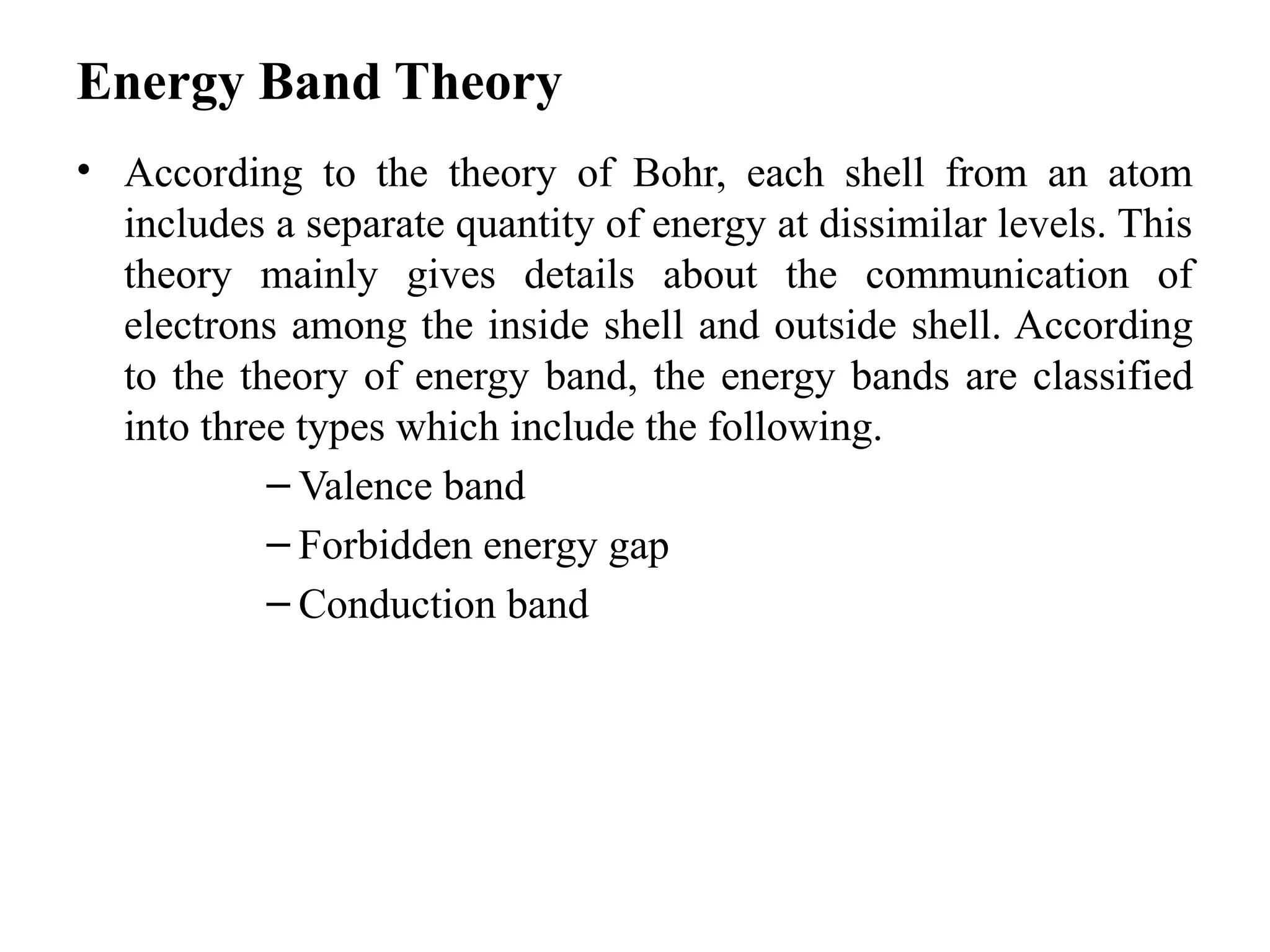
Energy Band Theory
•According to the theory of Bohr, each shell from an atom
includes a separate quantity of energy at dissimilar levels. This
theory mainly gives details about the communication of
electrons among the inside shell and outside shell. According
to the theory of energy band, the energy bands are classified
into three types which include the following.
– Valence band
– Forbidden energy gap
– Conduction band
4.
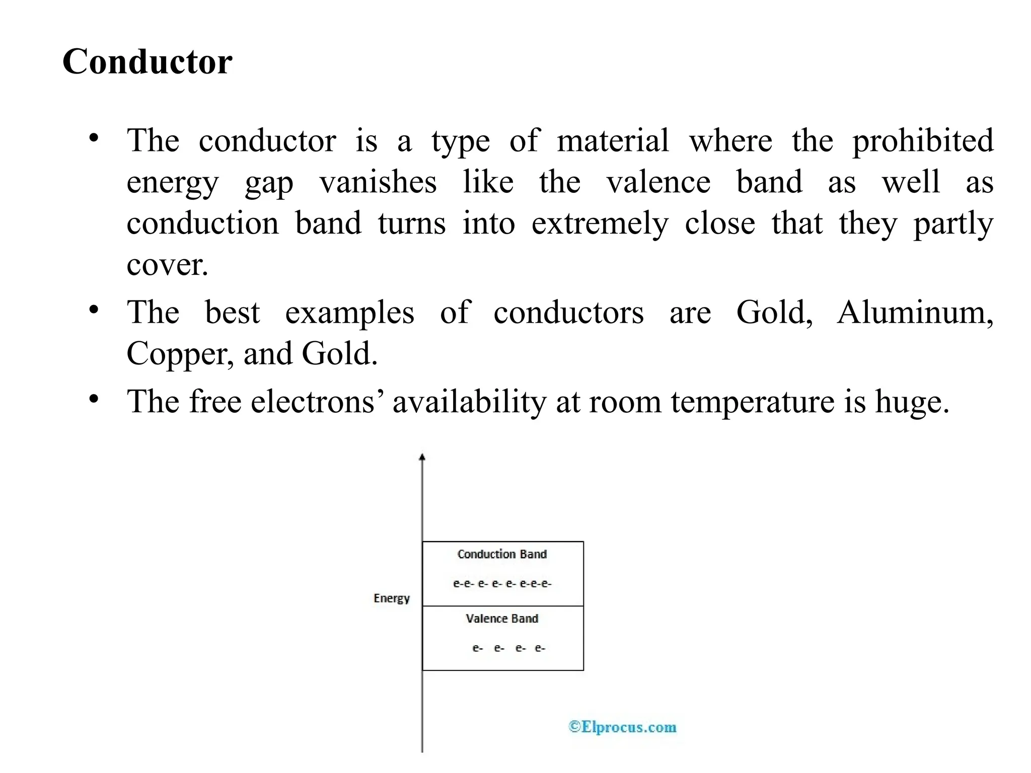
Conductor
• The conductoris a type of material where the prohibited
energy gap vanishes like the valence band as well as
conduction band turns into extremely close that they partly
cover.
• The best examples of conductors are Gold, Aluminum,
Copper, and Gold.
• The free electrons’ availability at room temperature is huge.
5.
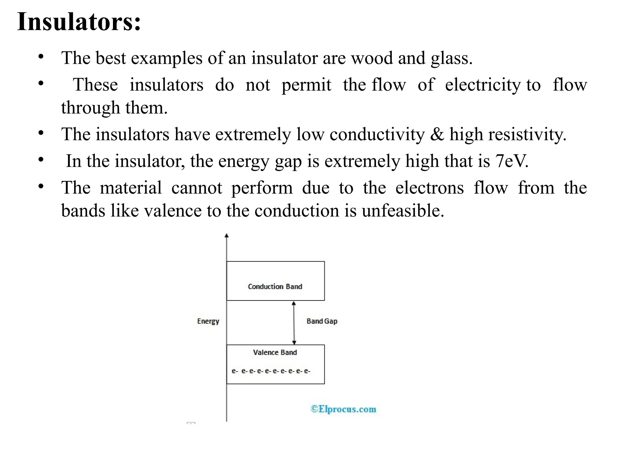
Insulators:
• The bestexamples of an insulator are wood and glass.
• These insulators do not permit the flow of electricity to flow
through them.
• The insulators have extremely low conductivity & high resistivity.
• In the insulator, the energy gap is extremely high that is 7eV.
• The material cannot perform due to the electrons flow from the
bands like valence to the conduction is unfeasible.
6.
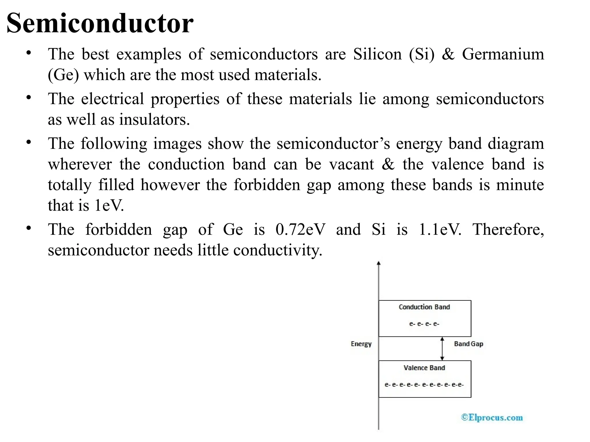
Semiconductor
• The bestexamples of semiconductors are Silicon (Si) & Germanium
(Ge) which are the most used materials.
• The electrical properties of these materials lie among semiconductors
as well as insulators.
• The following images show the semiconductor’s energy band diagram
wherever the conduction band can be vacant & the valence band is
totally filled however the forbidden gap among these bands is minute
that is 1eV.
• The forbidden gap of Ge is 0.72eV and Si is 1.1eV. Therefore,
semiconductor needs little conductivity.
7.
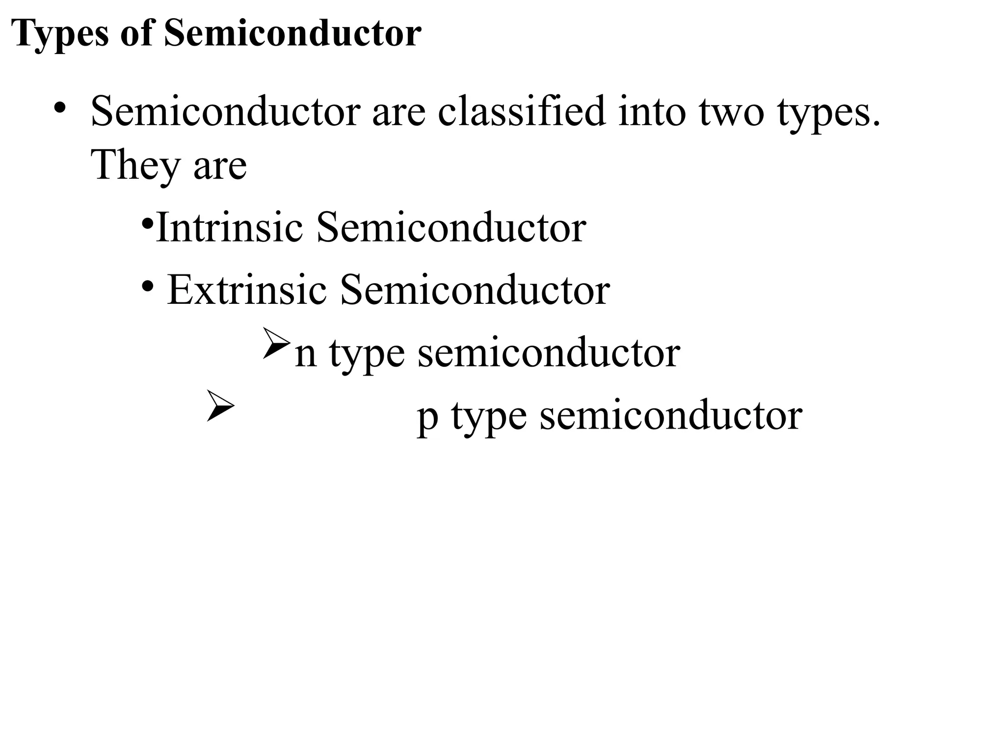
Types of Semiconductor
•Semiconductor are classified into two types.
They are
•Intrinsic Semiconductor
• Extrinsic Semiconductor
n type semiconductor
p type semiconductor
8.
Intrinsic Semiconductors
• Inintrinsic semiconductors, the number of free electrons, ne is
equal to the number of holes, nh . That is ne = nh = ni where ni is
called intrinsic carrier concentration.
• Semiconductors posses the unique property in which, apart
from electrons, the holes also move.
• This vacancy with the effective positive electronic charge is
called a hole. The hole behaves as an apparent free particle
with effective positive charge
9.
Extrinsic Semiconductors
• Theconductivity of an intrinsic semiconductor depends on its
temperature, but at room temperature its conductivity is very low.
• As such, no important electronic devices can be developed using
these semiconductors.
• Hence there is a necessity of improving their conductivity.
• This can be done by making use of impurities.
• Such materials are known as extrinsic semiconductors or impurity
semiconductors.
• The deliberate addition of a desirable impurity is called doping and
the impurity atoms are called dopants.
• Such a material is also called a doped semiconductor.
10.
N-type Semiconductors
• Thus,with proper level of doping the number of conduction
electrons can be made much larger than the number of holes.
• Hence in an extrinsic semiconductor doped with pentavalent
impurity, electrons become the majority carriers and holes the
minority carriers.
• These semiconductors are, therefore, known as n-type
semiconductors. .
• For n-type semiconductors, we have, ne >> nh
11.
P-type Semiconductors
• Inaddition to the intrinsically generated holes while the
source of conduction electrons is only intrinsic generation.
• Thus, for such a material, the holes are the majority
carriers and electrons are minority carriers.
• Therefore, extrinsic semiconductors doped with trivalent
impurity are called p-type semiconductors.
• For p-type semiconductors, the recombination process
will reduce the number (ni) of intrinsically generated
electrons to ne.
• We have, for p-type semiconductors nh >> ne
12.
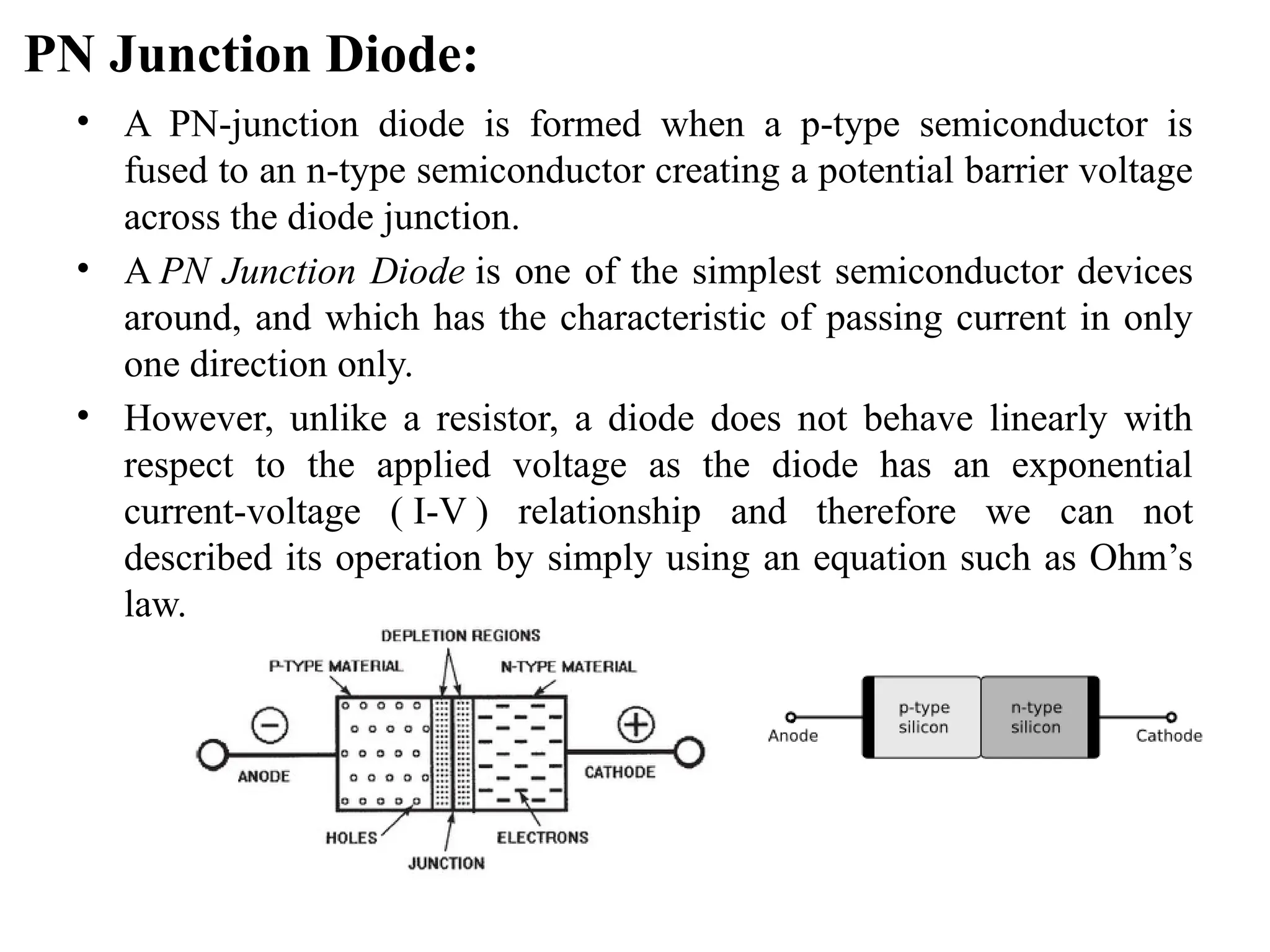
PN Junction Diode:
•A PN-junction diode is formed when a p-type semiconductor is
fused to an n-type semiconductor creating a potential barrier voltage
across the diode junction.
• A PN Junction Diode is one of the simplest semiconductor devices
around, and which has the characteristic of passing current in only
one direction only.
• However, unlike a resistor, a diode does not behave linearly with
respect to the applied voltage as the diode has an exponential
current-voltage ( I-V ) relationship and therefore we can not
described its operation by simply using an equation such as Ohm’s
law.
13.
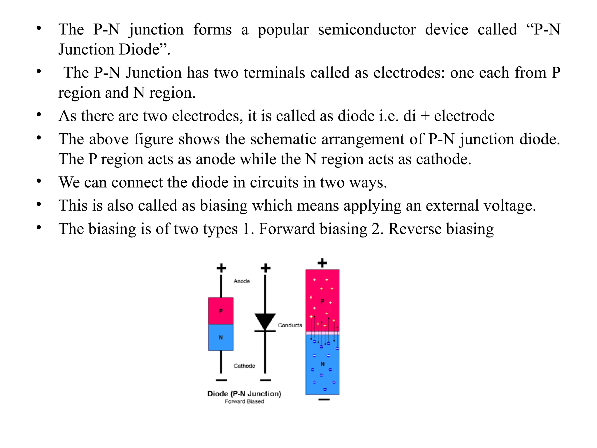
• The P-Njunction forms a popular semiconductor device called “P-N
Junction Diode”.
• The P-N Junction has two terminals called as electrodes: one each from P
region and N region.
• As there are two electrodes, it is called as diode i.e. di + electrode
• The above figure shows the schematic arrangement of P-N junction diode.
The P region acts as anode while the N region acts as cathode.
• We can connect the diode in circuits in two ways.
• This is also called as biasing which means applying an external voltage.
• The biasing is of two types 1. Forward biasing 2. Reverse biasing
14.
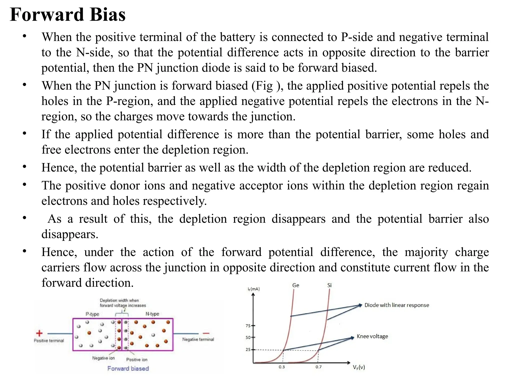
Forward Bias
• Whenthe positive terminal of the battery is connected to P-side and negative terminal
to the N-side, so that the potential difference acts in opposite direction to the barrier
potential, then the PN junction diode is said to be forward biased.
• When the PN junction is forward biased (Fig ), the applied positive potential repels the
holes in the P-region, and the applied negative potential repels the electrons in the N-
region, so the charges move towards the junction.
• If the applied potential difference is more than the potential barrier, some holes and
free electrons enter the depletion region.
• Hence, the potential barrier as well as the width of the depletion region are reduced.
• The positive donor ions and negative acceptor ions within the depletion region regain
electrons and holes respectively.
• As a result of this, the depletion region disappears and the potential barrier also
disappears.
• Hence, under the action of the forward potential difference, the majority charge
carriers flow across the junction in opposite direction and constitute current flow in the
forward direction.
15.
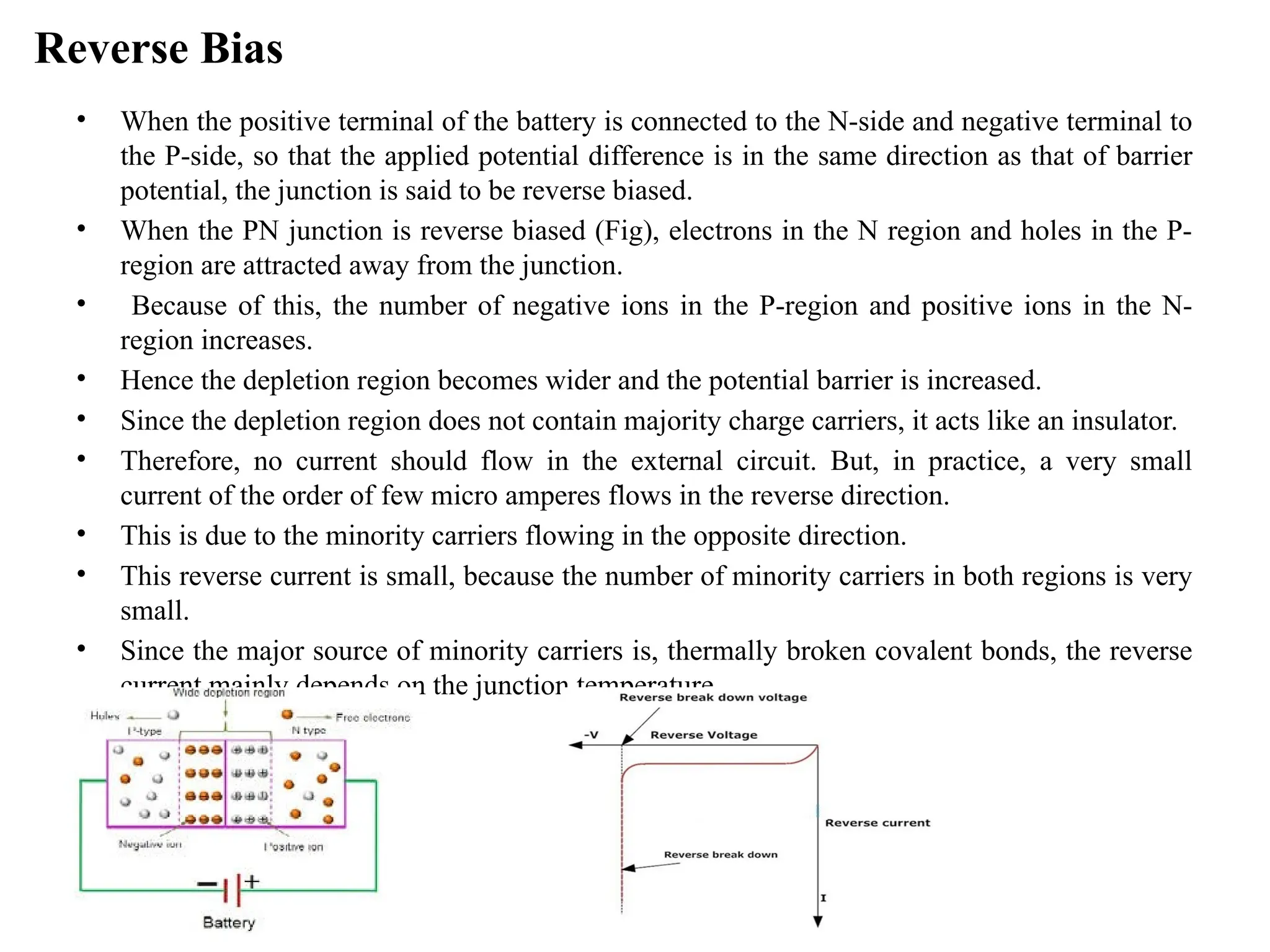
Reverse Bias
• Whenthe positive terminal of the battery is connected to the N-side and negative terminal to
the P-side, so that the applied potential difference is in the same direction as that of barrier
potential, the junction is said to be reverse biased.
• When the PN junction is reverse biased (Fig), electrons in the N region and holes in the P-
region are attracted away from the junction.
• Because of this, the number of negative ions in the P-region and positive ions in the N-
region increases.
• Hence the depletion region becomes wider and the potential barrier is increased.
• Since the depletion region does not contain majority charge carriers, it acts like an insulator.
• Therefore, no current should flow in the external circuit. But, in practice, a very small
current of the order of few micro amperes flows in the reverse direction.
• This is due to the minority carriers flowing in the opposite direction.
• This reverse current is small, because the number of minority carriers in both regions is very
small.
• Since the major source of minority carriers is, thermally broken covalent bonds, the reverse
current mainly depends on the junction temperature.
16.
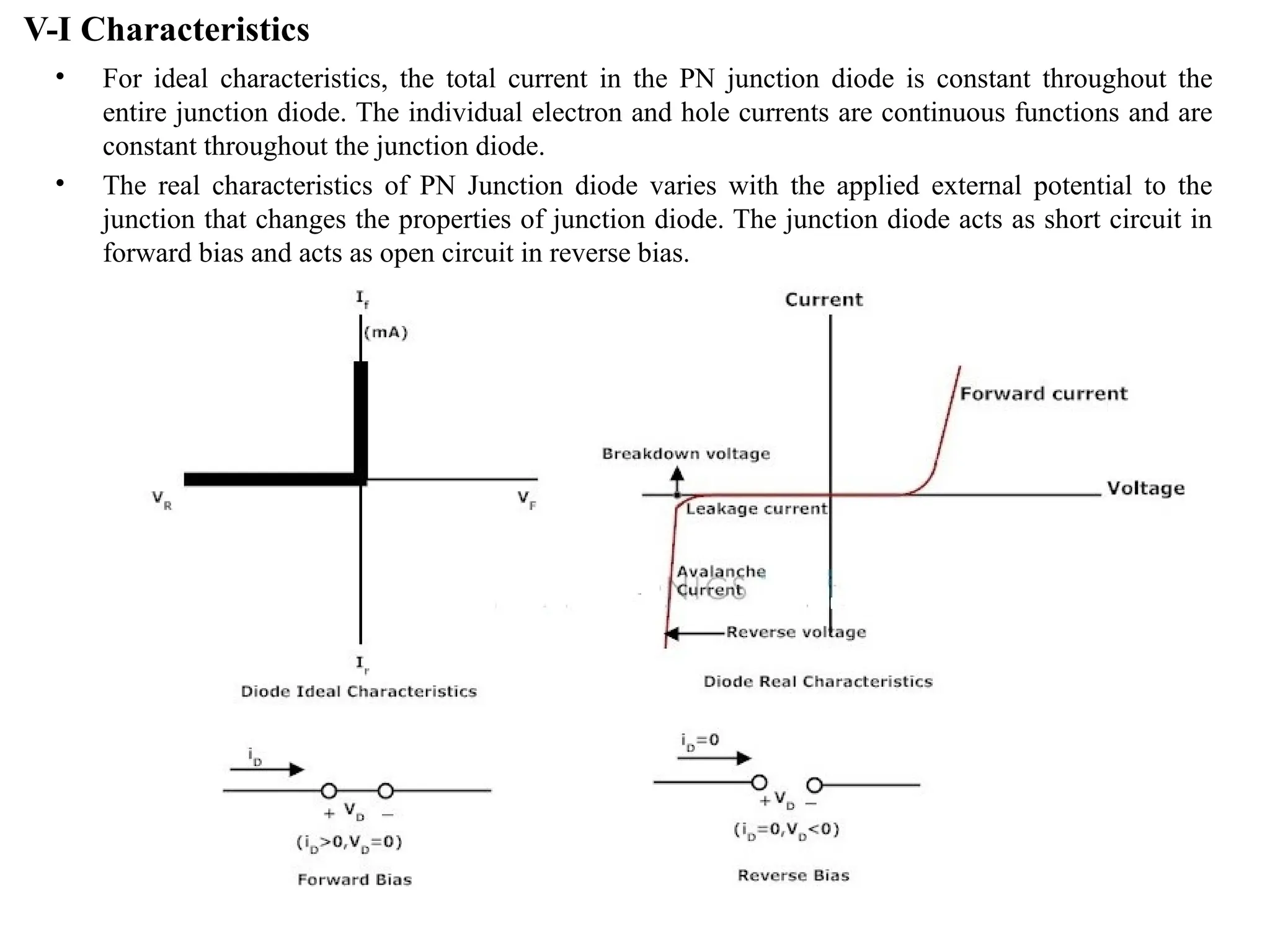
V-I Characteristics
• Forideal characteristics, the total current in the PN junction diode is constant throughout the
entire junction diode. The individual electron and hole currents are continuous functions and are
constant throughout the junction diode.
• The real characteristics of PN Junction diode varies with the applied external potential to the
junction that changes the properties of junction diode. The junction diode acts as short circuit in
forward bias and acts as open circuit in reverse bias.
17.
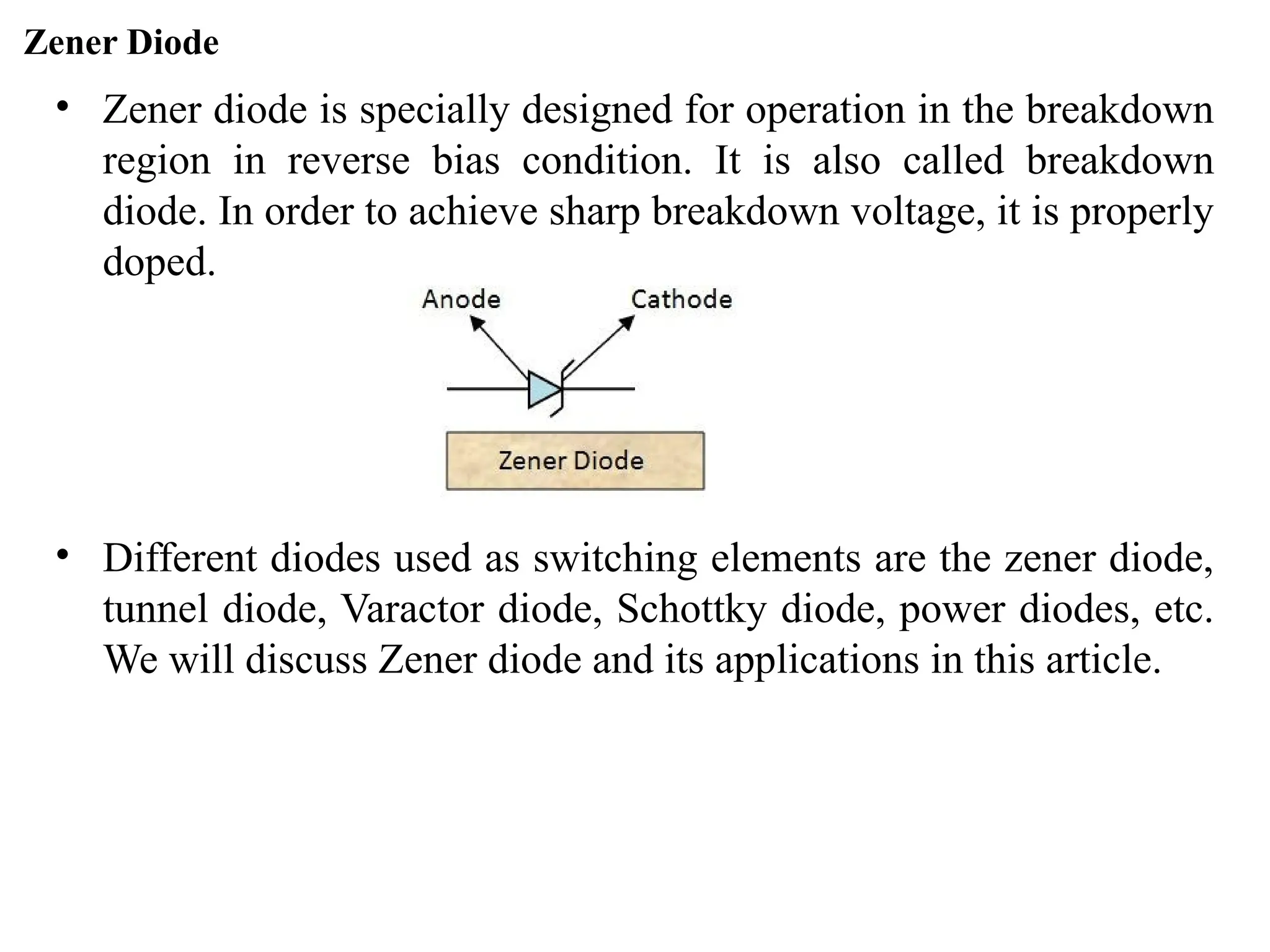
Zener Diode
• Zenerdiode is specially designed for operation in the breakdown
region in reverse bias condition. It is also called breakdown
diode. In order to achieve sharp breakdown voltage, it is properly
doped.
• Different diodes used as switching elements are the zener diode,
tunnel diode, Varactor diode, Schottky diode, power diodes, etc.
We will discuss Zener diode and its applications in this article.
18.
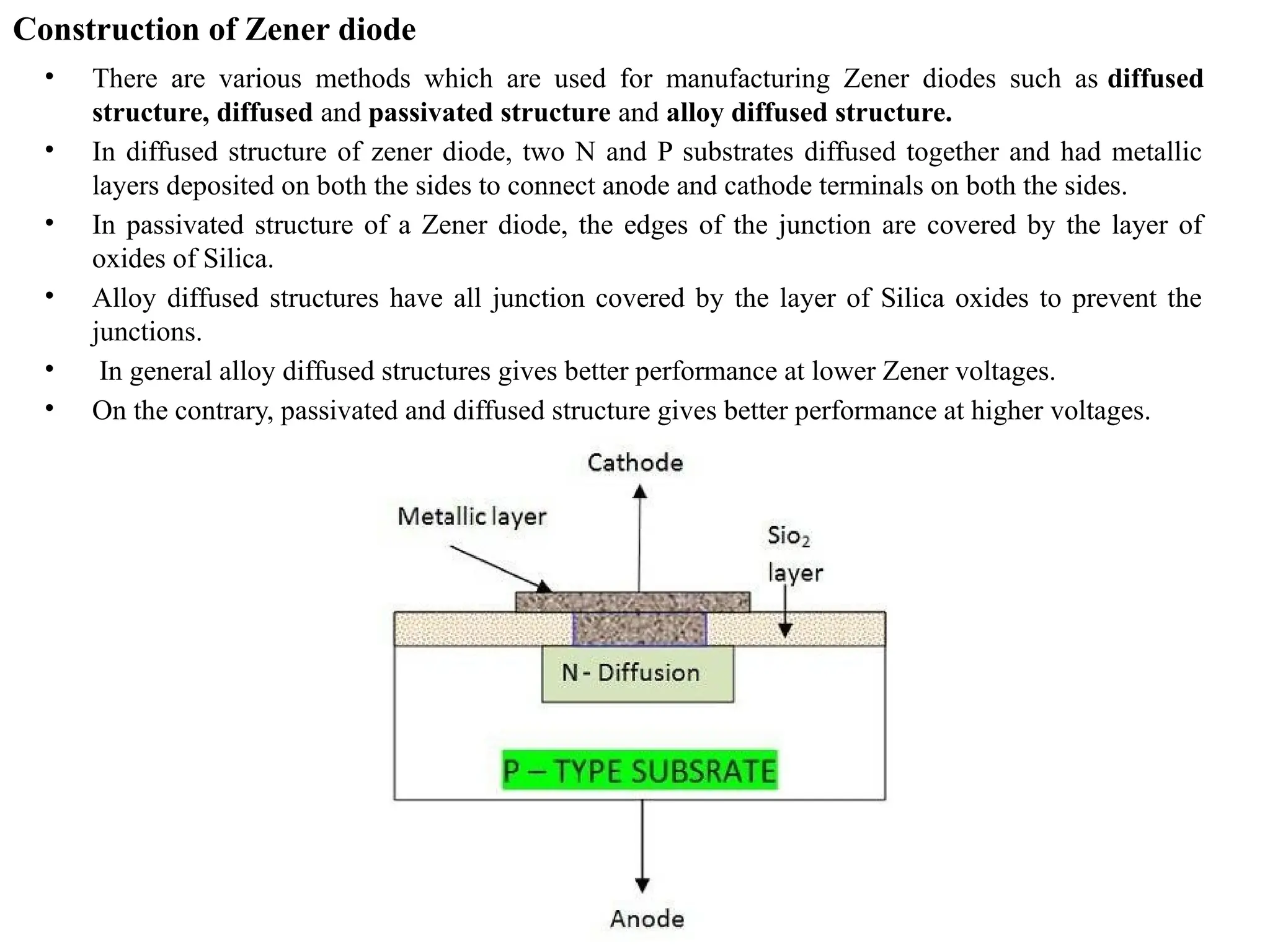
Construction of Zenerdiode
• There are various methods which are used for manufacturing Zener diodes such as diffused
structure, diffused and passivated structure and alloy diffused structure.
• In diffused structure of zener diode, two N and P substrates diffused together and had metallic
layers deposited on both the sides to connect anode and cathode terminals on both the sides.
• In passivated structure of a Zener diode, the edges of the junction are covered by the layer of
oxides of Silica.
• Alloy diffused structures have all junction covered by the layer of Silica oxides to prevent the
junctions.
• In general alloy diffused structures gives better performance at lower Zener voltages.
• On the contrary, passivated and diffused structure gives better performance at higher voltages.
19.
Working
• A Zenerdiode is similar to conventional PN Junction diode except that it is properly doped to
achieve sharp breakdown voltage. There are two types of mechanism by which breakdown can
occur at reverse PN junction that are avalanche and Zener breakdown.
Zener Breakdown
• Zener breakdown occurs due to high reverse Voltage. When the high reverse voltage is applied the
width of depletion layer increases. Due to this potential barrier increases and a high electric field is
generated at the junction. This high electric field breaks the covalent bond and a large number of
minority charge carrier are generated.
• Thus, current increases suddenly due to the movement of minority charge carriers and sometimes it
leads to the breakdown of the junction. This is called of Zener breakdown. This is observed in
diodes having a reverse voltage of less than 5 volts.
Avalanche Breakdown
• Avalanche Breakdown mechanism comes into picture when the reverse voltage becomes extremely
high. At such a high reverse voltage, the minority carriers get extremely high kinetic energy. Due to
which they easily detach electrons from the covalent bond.
• Thus, these free electrons, in turn, collide with other atoms to liberate more electrons. In this way,
the current becomes very large that it leads to the breakdown of the diode. Avalanche
breakdown occurs when the reverse voltage becomes higher than 5V.
• A Zener diode can use any of these two breakdown mechanisms. Although there are two types of
breakdown mechanism, still only name Zener is preferred. Silicon and Germanium both can be used
for the construction of Zener diode, but Silicon is often used because of it can operate at higher
temperature, and current capability of silicon is high.
20.
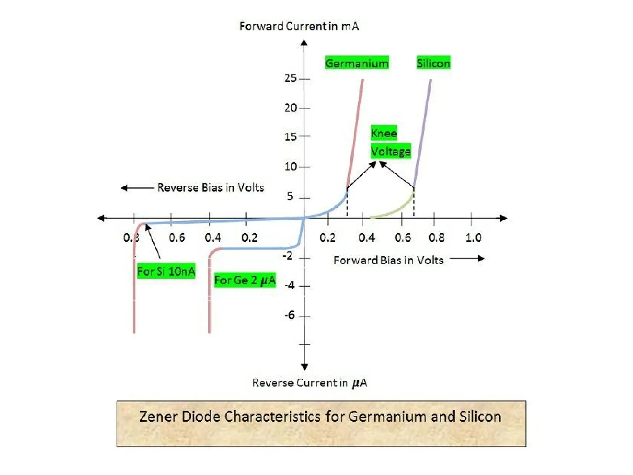
V-I Characteristics
• Wehave already discussed earlier that when the reverse voltage increases at a particular
point, the junction breakdowns due to large reverse current.
• The voltage at which current starts increasing rapidly and the stage of breakdown is
reached it is called Zener Voltage. The current which increases rapidly is called Zener
Current.
• The diagram represents the Volt-Ampere Characteristics of Silicon and Germanium
diodes. It is operated in breakdown region, and the current is limited by dynamic
resistance called zener impedance.
• The magnitude of zener voltage is dependent on the amount of doping.
• The forward Characteristics of Zener diode is similar to that of ordinary PN Junction
Diode. But the reverse characteristics are slightly different. During the operation in
breakdown region, it does not burn out immediately.
• As long as the current through the diode is limited by the external circuit within
permissible values, it does not burn out.
• A heavily doped diode will have very thin depletion layer. Thus, Zener voltage will be
very low. In this way, depletion layer and zener voltage can be controlled with the help
of doping concentration.
• Zener impedance: It is the dynamic resistance of a zener diode. It is represented by rz .
rz = ΔVz / Δ Iz
22.
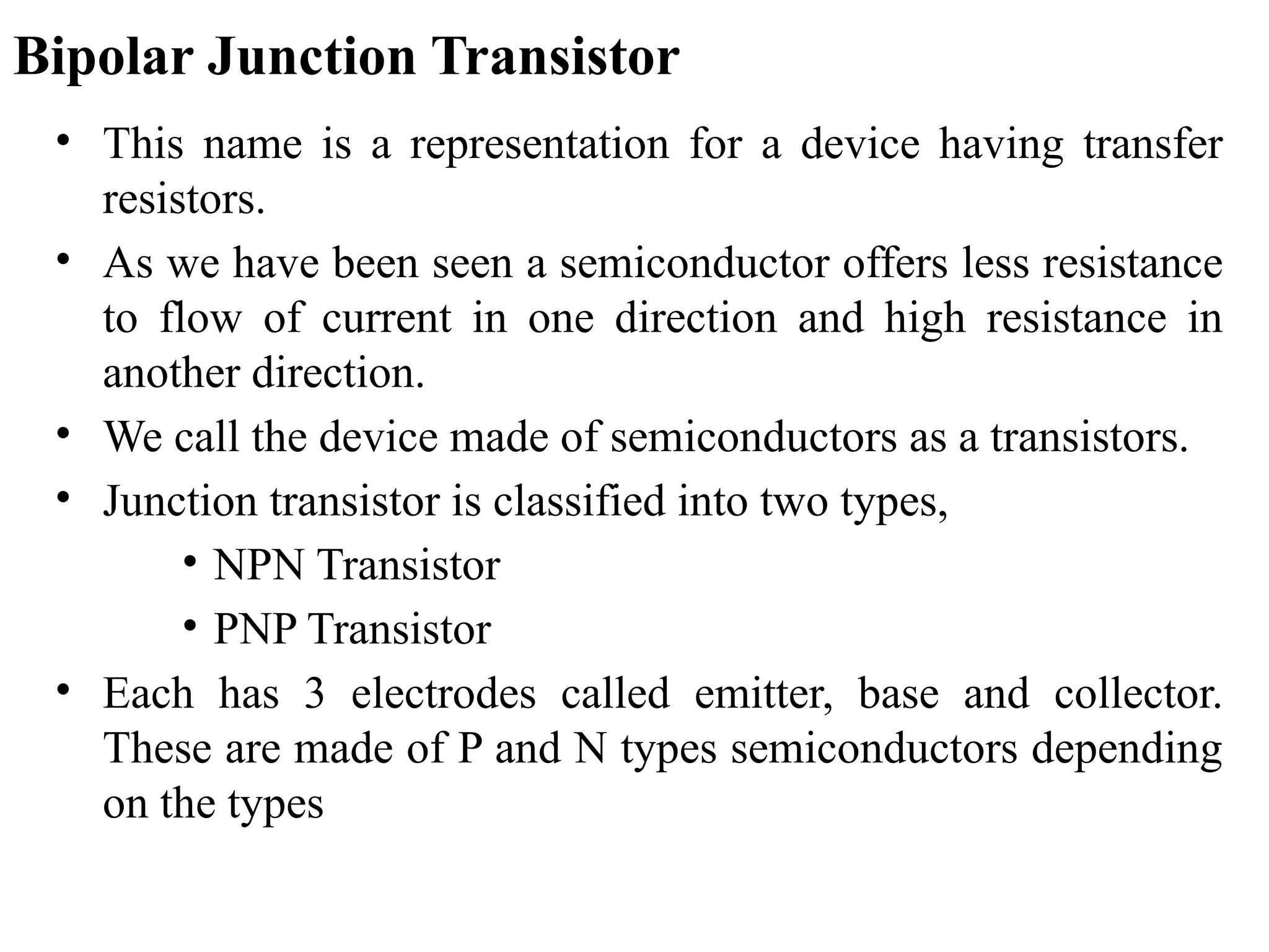
Bipolar Junction Transistor
•This name is a representation for a device having transfer
resistors.
• As we have been seen a semiconductor offers less resistance
to flow of current in one direction and high resistance in
another direction.
• We call the device made of semiconductors as a transistors.
• Junction transistor is classified into two types,
• NPN Transistor
• PNP Transistor
• Each has 3 electrodes called emitter, base and collector.
These are made of P and N types semiconductors depending
on the types
23.
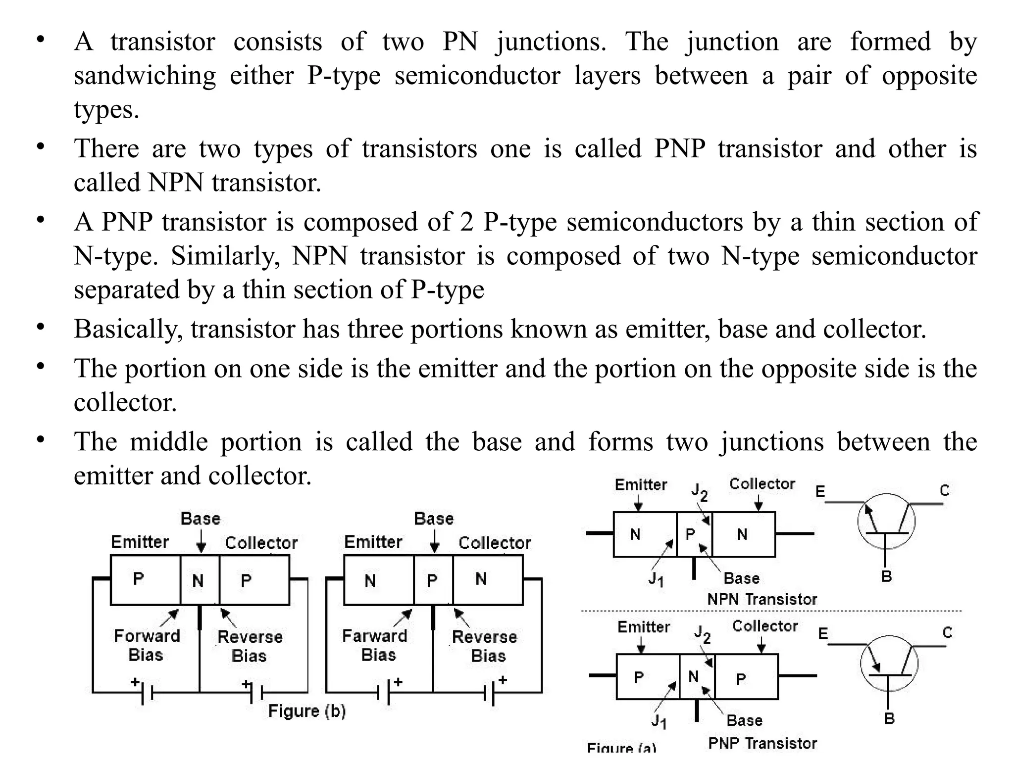
• A transistorconsists of two PN junctions. The junction are formed by
sandwiching either P-type semiconductor layers between a pair of opposite
types.
• There are two types of transistors one is called PNP transistor and other is
called NPN transistor.
• A PNP transistor is composed of 2 P-type semiconductors by a thin section of
N-type. Similarly, NPN transistor is composed of two N-type semiconductor
separated by a thin section of P-type
• Basically, transistor has three portions known as emitter, base and collector.
• The portion on one side is the emitter and the portion on the opposite side is the
collector.
• The middle portion is called the base and forms two junctions between the
emitter and collector.
25.
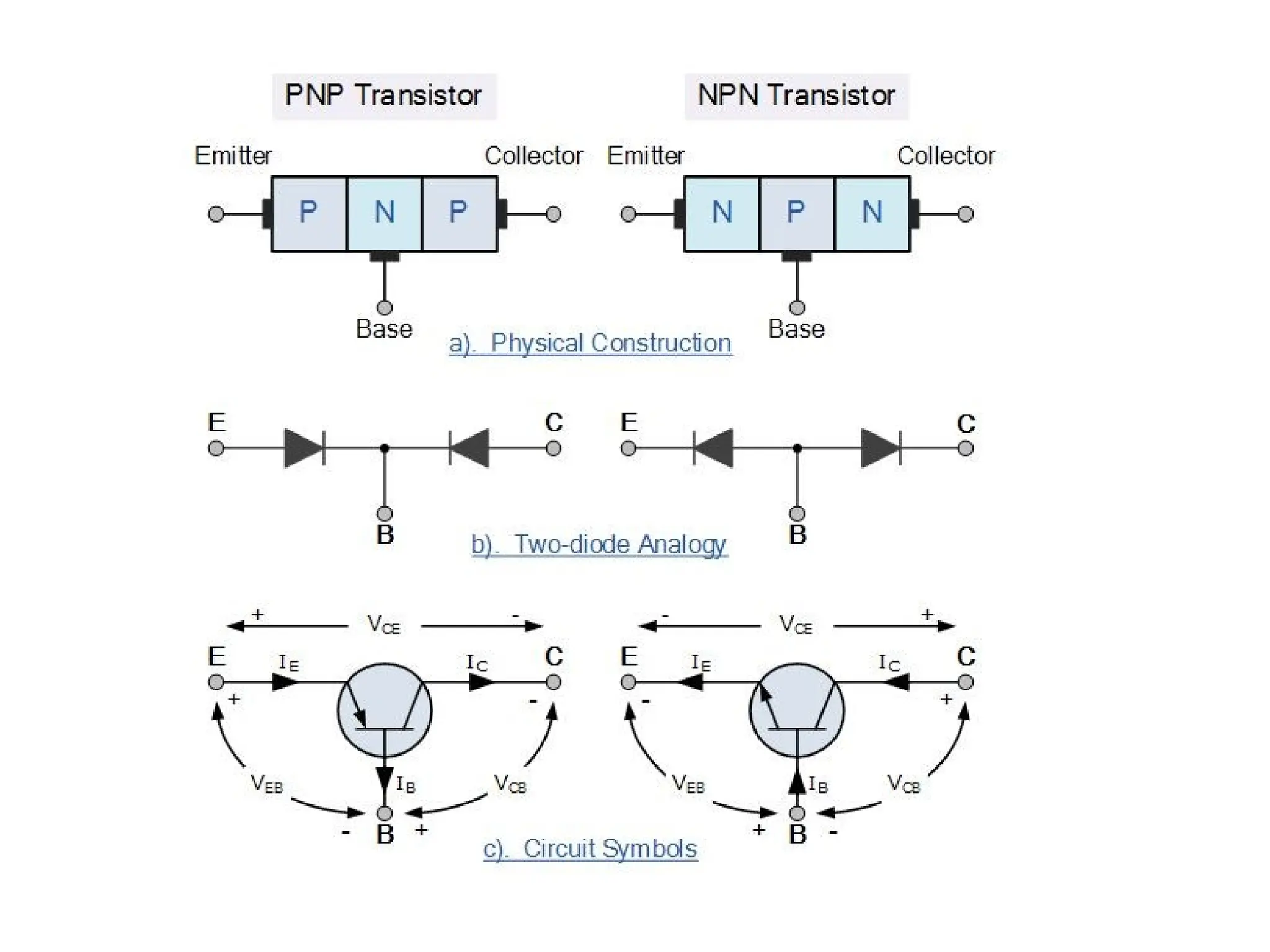
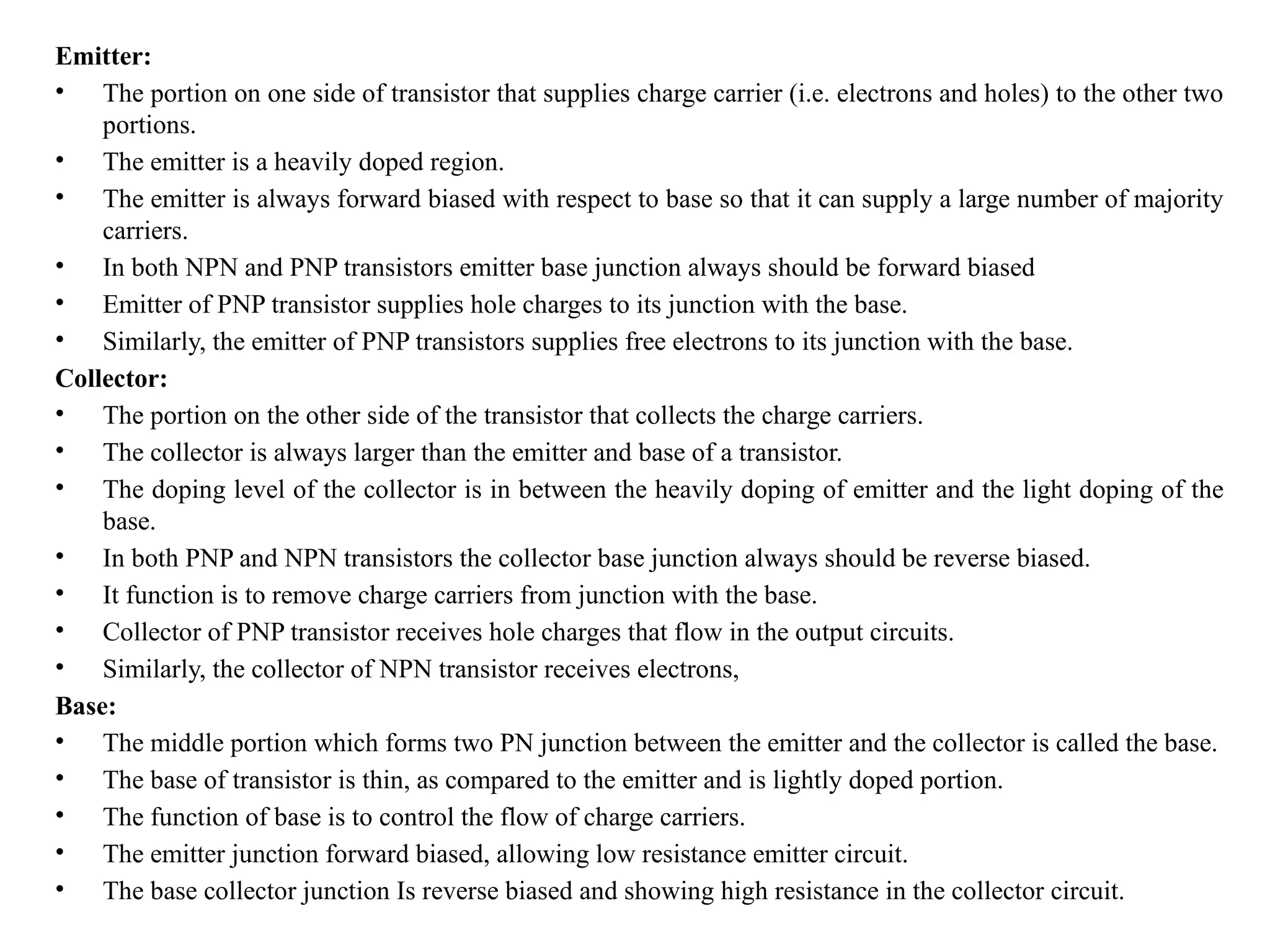
Emitter:
• The portionon one side of transistor that supplies charge carrier (i.e. electrons and holes) to the other two
portions.
• The emitter is a heavily doped region.
• The emitter is always forward biased with respect to base so that it can supply a large number of majority
carriers.
• In both NPN and PNP transistors emitter base junction always should be forward biased
• Emitter of PNP transistor supplies hole charges to its junction with the base.
• Similarly, the emitter of PNP transistors supplies free electrons to its junction with the base.
Collector:
• The portion on the other side of the transistor that collects the charge carriers.
• The collector is always larger than the emitter and base of a transistor.
• The doping level of the collector is in between the heavily doping of emitter and the light doping of the
base.
• In both PNP and NPN transistors the collector base junction always should be reverse biased.
• It function is to remove charge carriers from junction with the base.
• Collector of PNP transistor receives hole charges that flow in the output circuits.
• Similarly, the collector of NPN transistor receives electrons,
Base:
• The middle portion which forms two PN junction between the emitter and the collector is called the base.
• The base of transistor is thin, as compared to the emitter and is lightly doped portion.
• The function of base is to control the flow of charge carriers.
• The emitter junction forward biased, allowing low resistance emitter circuit.
• The base collector junction Is reverse biased and showing high resistance in the collector circuit.
26.
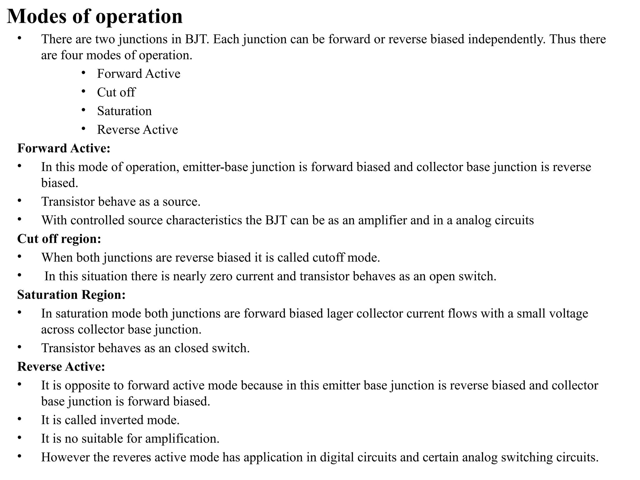
Modes of operation
•There are two junctions in BJT. Each junction can be forward or reverse biased independently. Thus there
are four modes of operation.
• Forward Active
• Cut off
• Saturation
• Reverse Active
Forward Active:
• In this mode of operation, emitter-base junction is forward biased and collector base junction is reverse
biased.
• Transistor behave as a source.
• With controlled source characteristics the BJT can be as an amplifier and in a analog circuits
Cut off region:
• When both junctions are reverse biased it is called cutoff mode.
• In this situation there is nearly zero current and transistor behaves as an open switch.
Saturation Region:
• In saturation mode both junctions are forward biased lager collector current flows with a small voltage
across collector base junction.
• Transistor behaves as an closed switch.
Reverse Active:
• It is opposite to forward active mode because in this emitter base junction is reverse biased and collector
base junction is forward biased.
• It is called inverted mode.
• It is no suitable for amplification.
• However the reveres active mode has application in digital circuits and certain analog switching circuits.
27.
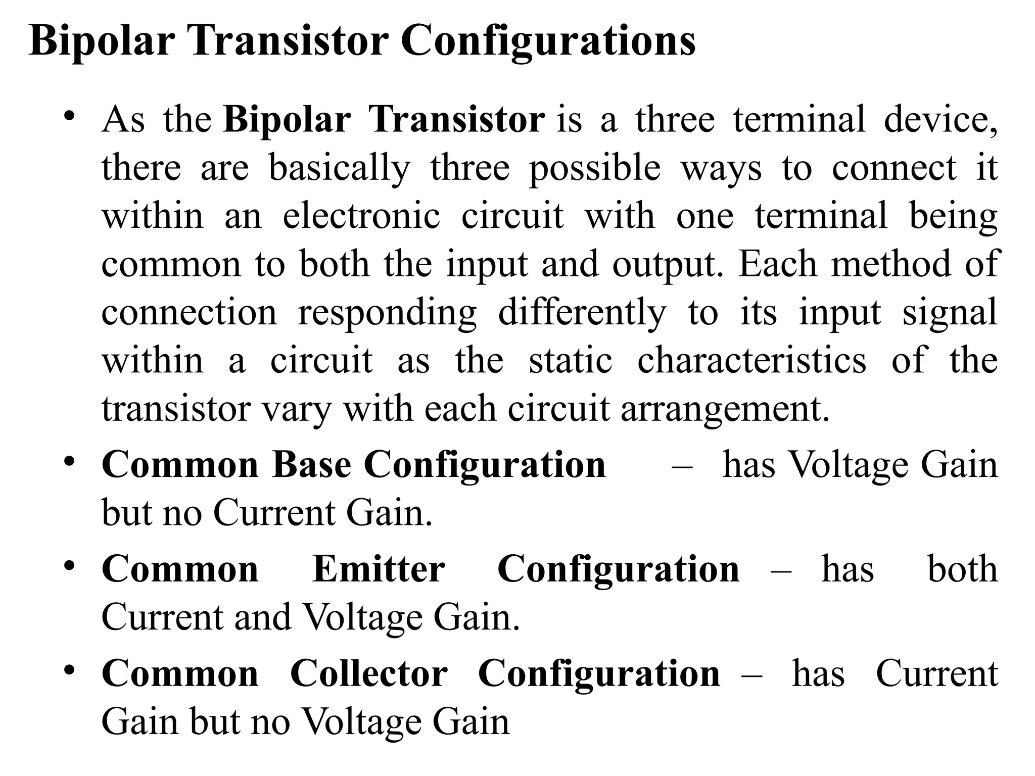
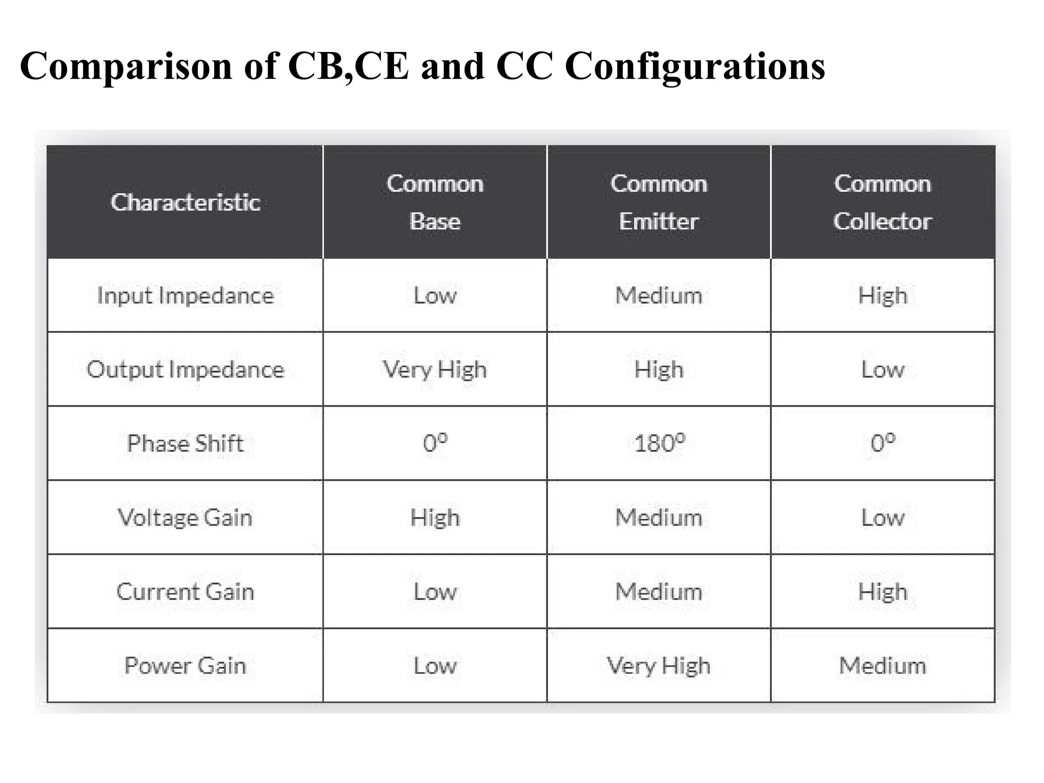
Bipolar Transistor Configurations
•As the Bipolar Transistor is a three terminal device,
there are basically three possible ways to connect it
within an electronic circuit with one terminal being
common to both the input and output. Each method of
connection responding differently to its input signal
within a circuit as the static characteristics of the
transistor vary with each circuit arrangement.
• Common Base Configuration – has Voltage Gain
but no Current Gain.
• Common Emitter Configuration – has both
Current and Voltage Gain.
• Common Collector Configuration – has Current
Gain but no Voltage Gain
28.
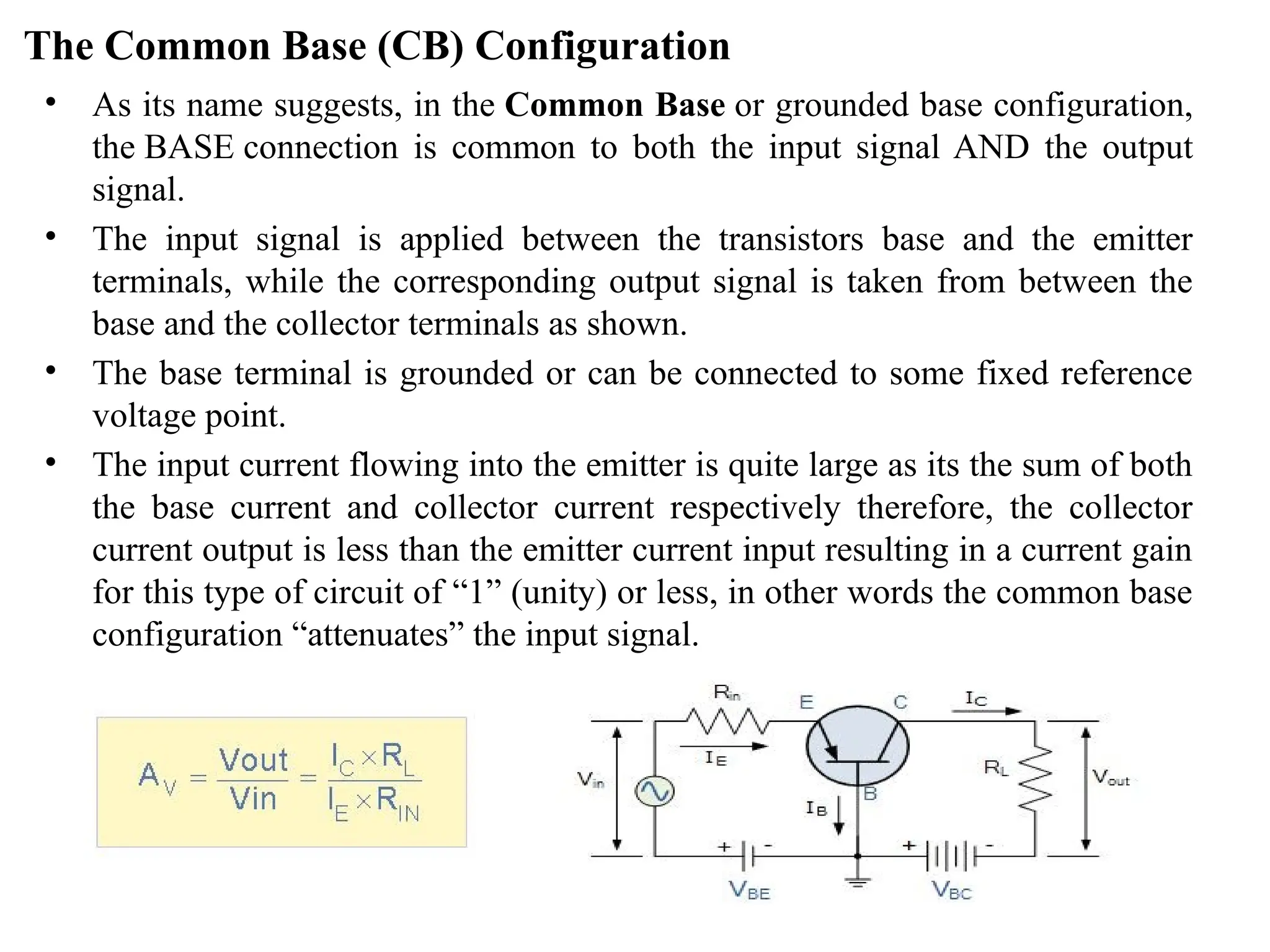
The Common Base(CB) Configuration
• As its name suggests, in the Common Base or grounded base configuration,
the BASE connection is common to both the input signal AND the output
signal.
• The input signal is applied between the transistors base and the emitter
terminals, while the corresponding output signal is taken from between the
base and the collector terminals as shown.
• The base terminal is grounded or can be connected to some fixed reference
voltage point.
• The input current flowing into the emitter is quite large as its the sum of both
the base current and collector current respectively therefore, the collector
current output is less than the emitter current input resulting in a current gain
for this type of circuit of “1” (unity) or less, in other words the common base
configuration “attenuates” the input signal.
29.
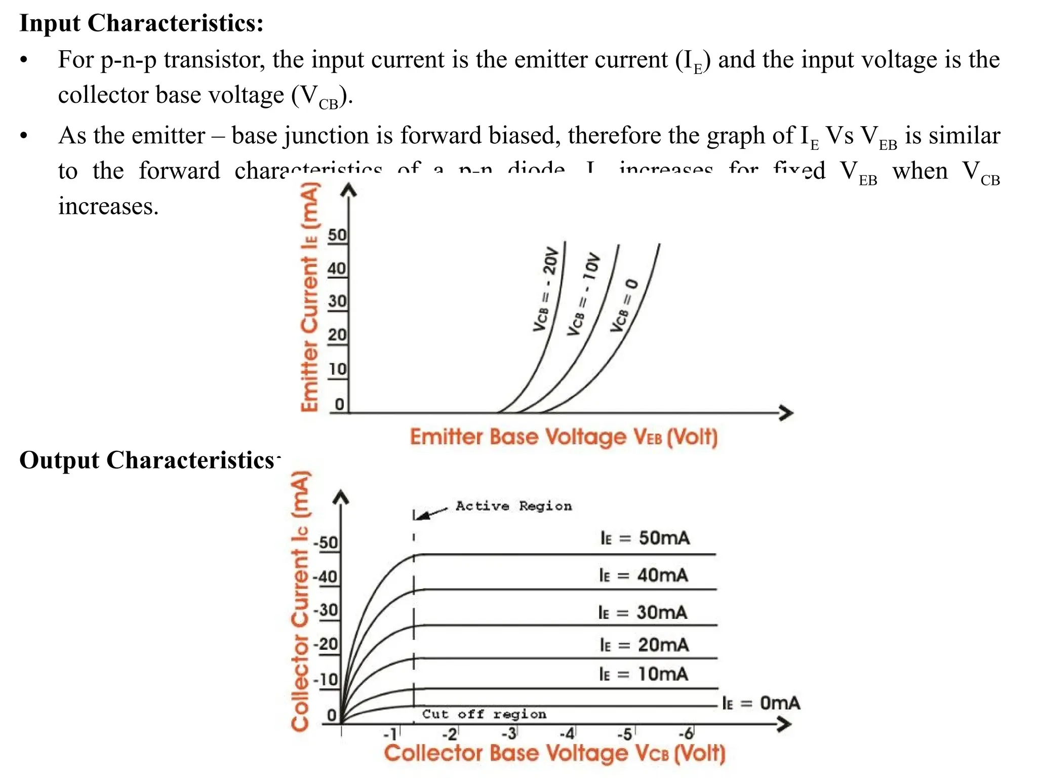
Input Characteristics:
• Forp-n-p transistor, the input current is the emitter current (IE) and the input voltage is the
collector base voltage (VCB).
• As the emitter – base junction is forward biased, therefore the graph of IE Vs VEB is similar
to the forward characteristics of a p-n diode. IE increases for fixed VEB when VCB
increases.
Output Characteristics:
30.
• The outputcharacteristics shows the relation between output
voltage and output current IC is the output current and collector-
base voltage and the emitter current IE is the input current and
works as the parameters.
• As we know for p-n-p transistors IE and VEB are positive and IC,
IB, VCB are negative.
• These are three regions in the curve, active region saturation
region and the cut off region.
• The active region is the region where the transistor operates
normally. Here the emitter junction is reverse biased.
• Now the saturation region is the region where both the emitter
collector junctions are forward biased.
• And finally the cut off region is the region where both emitter and
the collector junctions are reverse biased.
31.
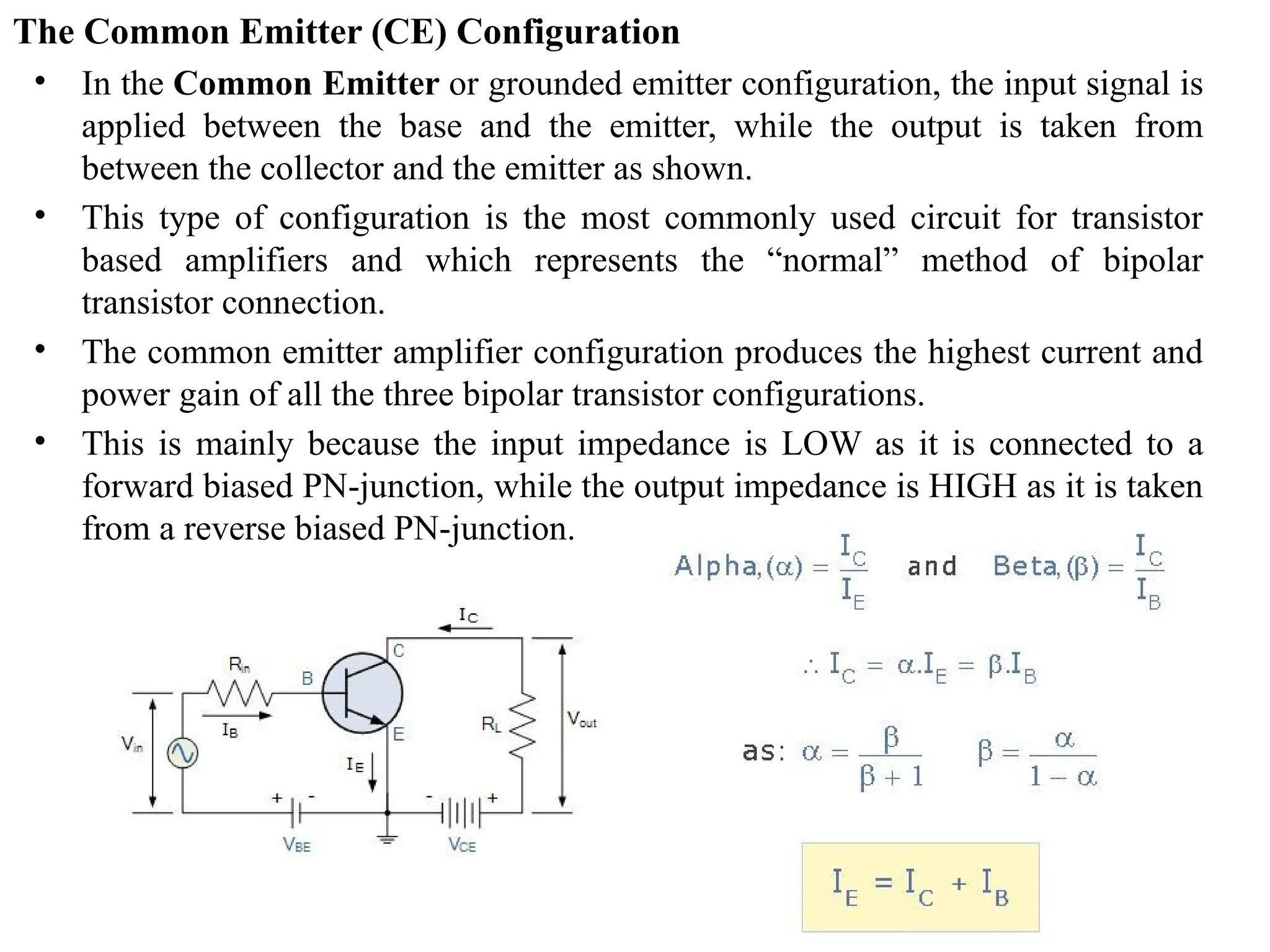
The Common Emitter(CE) Configuration
• In the Common Emitter or grounded emitter configuration, the input signal is
applied between the base and the emitter, while the output is taken from
between the collector and the emitter as shown.
• This type of configuration is the most commonly used circuit for transistor
based amplifiers and which represents the “normal” method of bipolar
transistor connection.
• The common emitter amplifier configuration produces the highest current and
power gain of all the three bipolar transistor configurations.
• This is mainly because the input impedance is LOW as it is connected to a
forward biased PN-junction, while the output impedance is HIGH as it is taken
from a reverse biased PN-junction.
32.
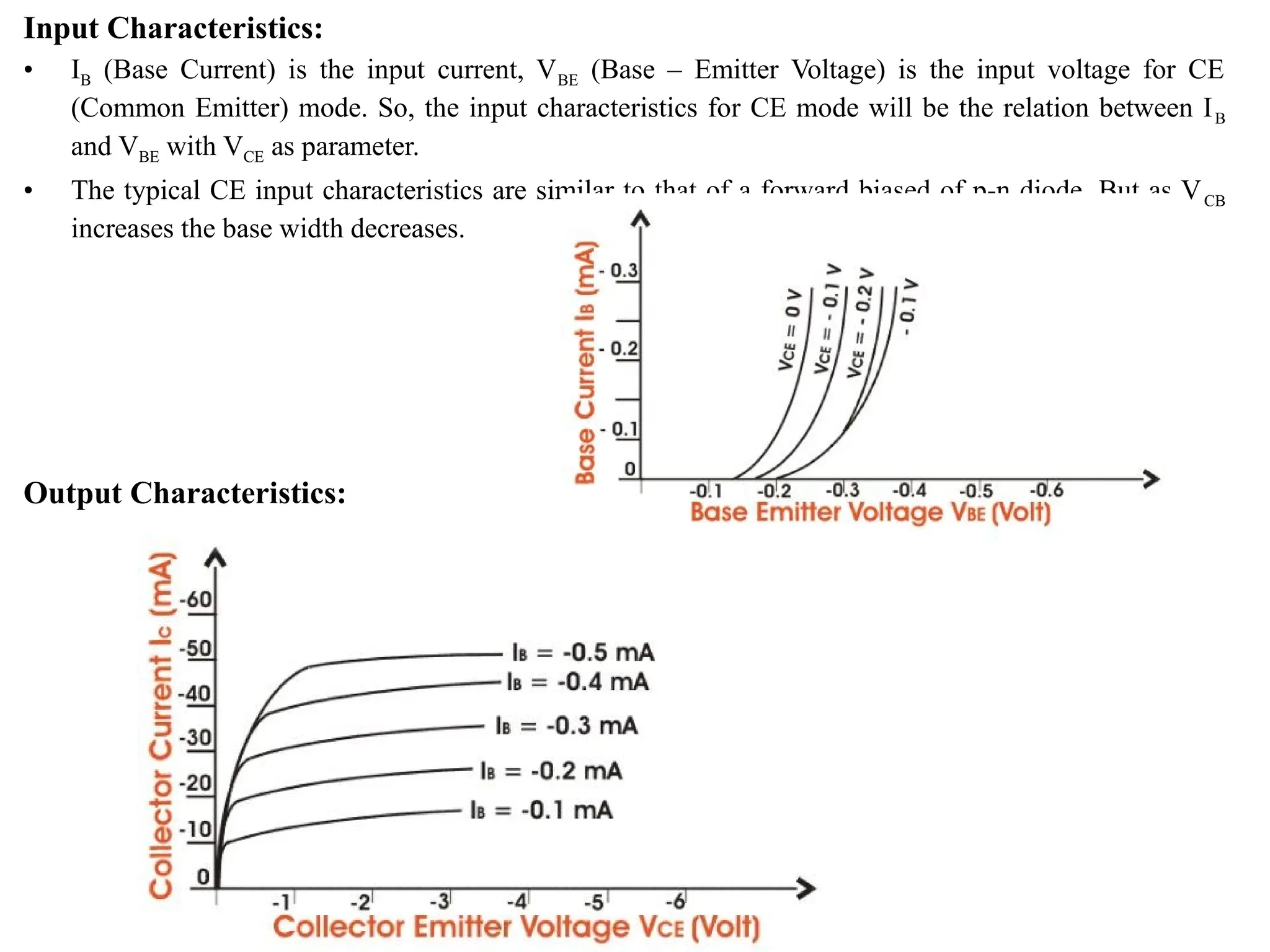
Input Characteristics:
• IB(Base Current) is the input current, VBE (Base – Emitter Voltage) is the input voltage for CE
(Common Emitter) mode. So, the input characteristics for CE mode will be the relation between IB
and VBE with VCE as parameter.
• The typical CE input characteristics are similar to that of a forward biased of p-n diode. But as VCB
increases the base width decreases.
Output Characteristics:
33.
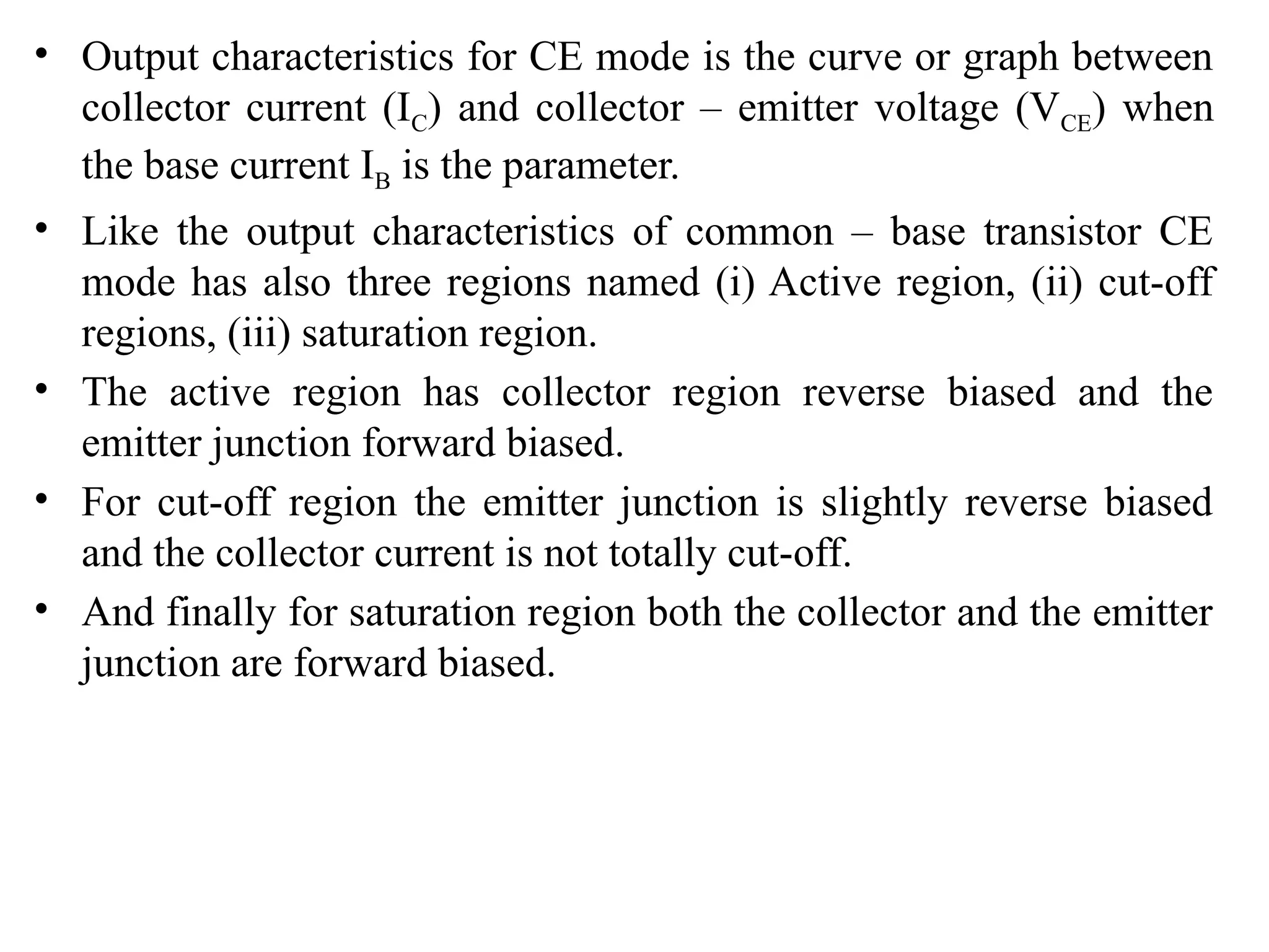
• Output characteristicsfor CE mode is the curve or graph between
collector current (IC) and collector – emitter voltage (VCE) when
the base current IB is the parameter.
• Like the output characteristics of common – base transistor CE
mode has also three regions named (i) Active region, (ii) cut-off
regions, (iii) saturation region.
• The active region has collector region reverse biased and the
emitter junction forward biased.
• For cut-off region the emitter junction is slightly reverse biased
and the collector current is not totally cut-off.
• And finally for saturation region both the collector and the emitter
junction are forward biased.
34.
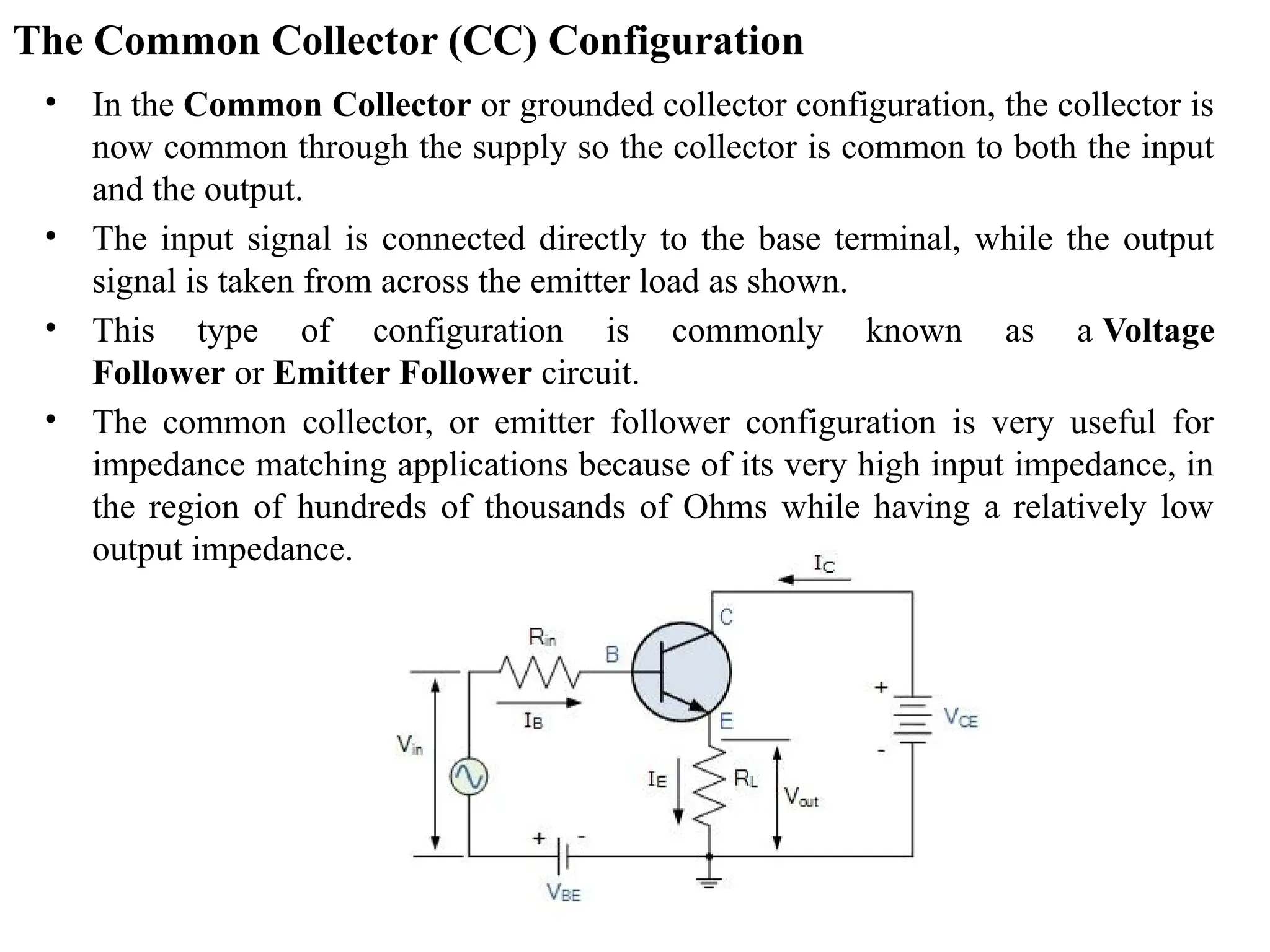
The Common Collector(CC) Configuration
• In the Common Collector or grounded collector configuration, the collector is
now common through the supply so the collector is common to both the input
and the output.
• The input signal is connected directly to the base terminal, while the output
signal is taken from across the emitter load as shown.
• This type of configuration is commonly known as a Voltage
Follower or Emitter Follower circuit.
• The common collector, or emitter follower configuration is very useful for
impedance matching applications because of its very high input impedance, in
the region of hundreds of thousands of Ohms while having a relatively low
output impedance.
35.
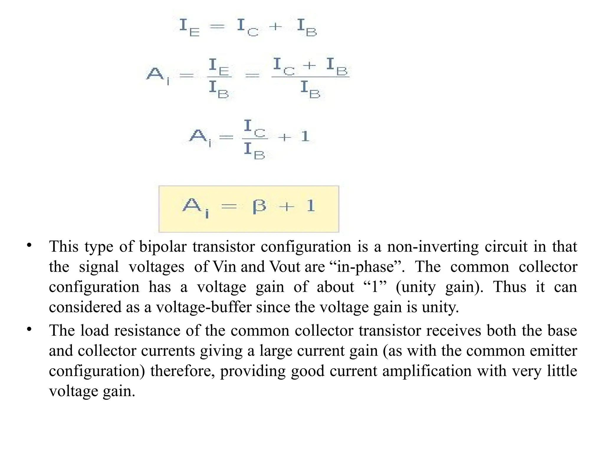
• This typeof bipolar transistor configuration is a non-inverting circuit in that
the signal voltages of Vin and Vout are “in-phase”. The common collector
configuration has a voltage gain of about “1” (unity gain). Thus it can
considered as a voltage-buffer since the voltage gain is unity.
• The load resistance of the common collector transistor receives both the base
and collector currents giving a large current gain (as with the common emitter
configuration) therefore, providing good current amplification with very little
voltage gain.
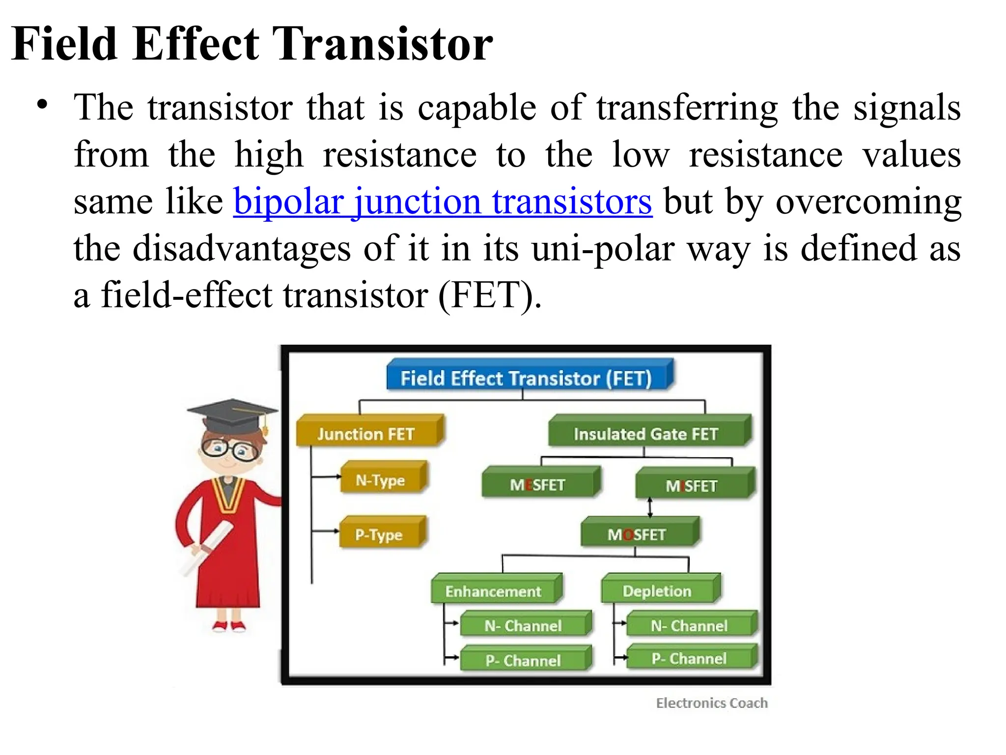
Field Effect Transistor
•The transistor that is capable of transferring the signals
from the high resistance to the low resistance values
same like bipolar junction transistors but by overcoming
the disadvantages of it in its uni-polar way is defined as
a field-effect transistor (FET).
38.
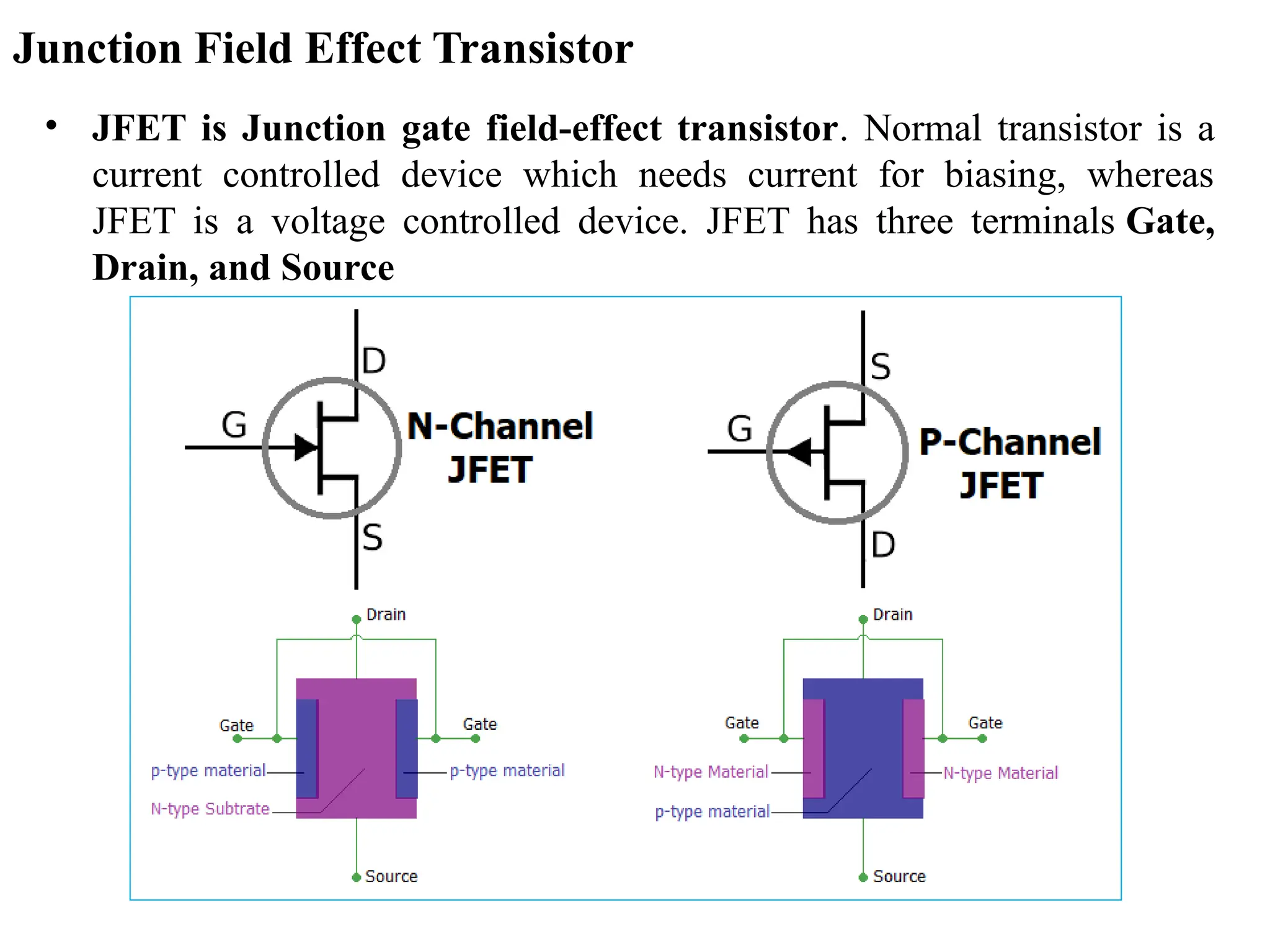
Junction Field EffectTransistor
• JFET is Junction gate field-effect transistor. Normal transistor is a
current controlled device which needs current for biasing, whereas
JFET is a voltage controlled device. JFET has three terminals Gate,
Drain, and Source
39.
• The arrowdenotes the types of JFET.
• The arrow showing to the gate denotes that the JFET is N-channel and on the
other hand the arrow from the gate denotes P-channel JFET.
• This arrow also indicates the polarity of P-N junction, which is formed
between the channel and the gate.
• The current flowing through the Drain and Source is dependable on the
voltage applied to the Gate terminal.
• For the N channel JFET, the Gate voltage is negative and for the P channel
JFET the Gate voltage is positive.
• The N-Channel JFET consists of P-type material in N-type substrate whereas
N-type materials are used in the p-type substrate to form a P channel JFET.
• JFET is constructed using the long channel of semiconductor material.
• Depending on the construction process, if the JFET contains a great number
of positive charge carriers (refers as holes) is a P-type JFET, and if it has a
large number of negative charge carriers (refers as electrons) is called N-type
JFET.
• In the long channel of semiconductor material, Ohmic contacts at each end
are created to form the Source and Drain connections.
• A P-N junction is formed in one or both side of the channel.
40.
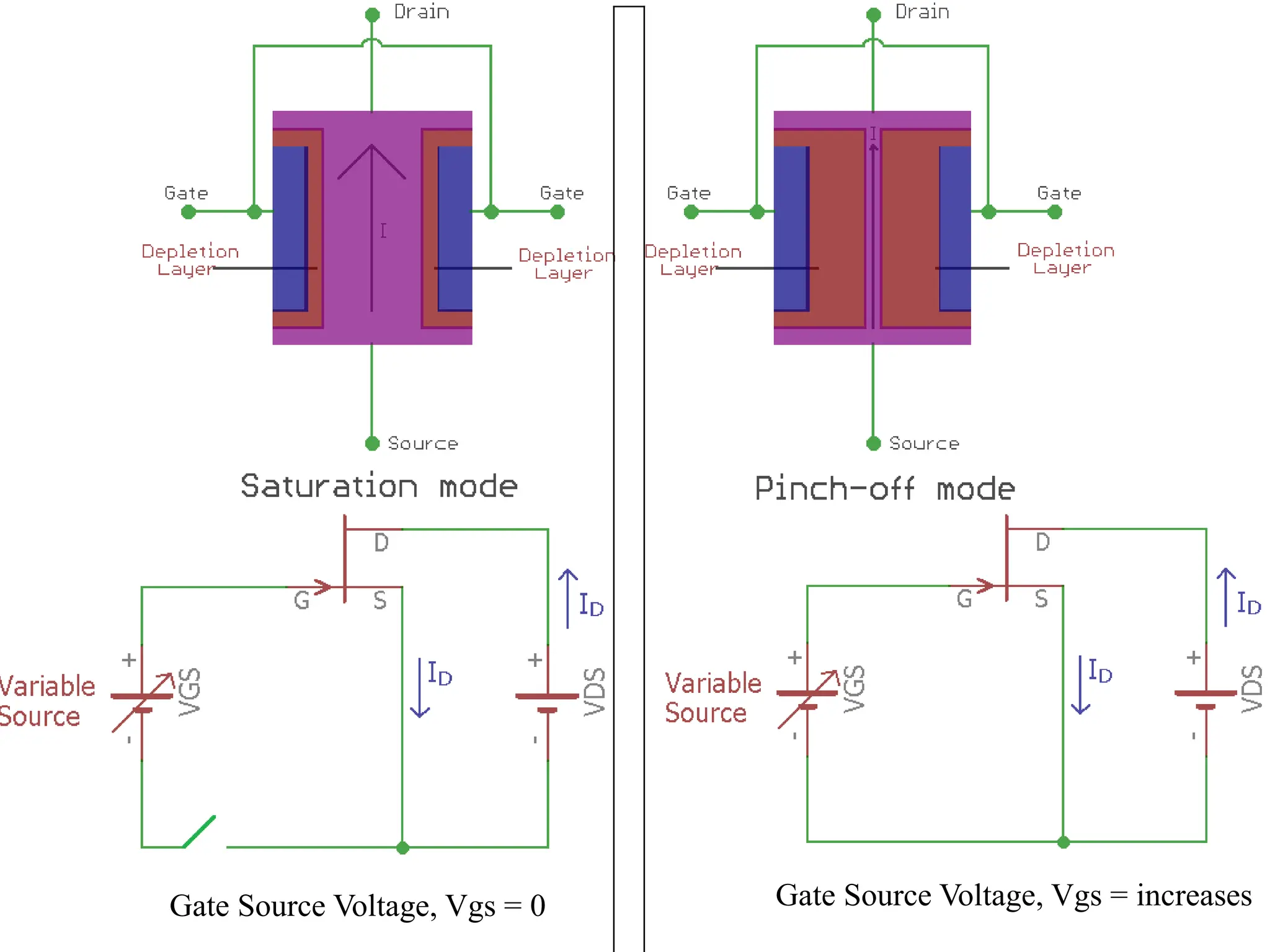
Working:
• One bestexample to understand the working of a JFET is to imagine the garden hose
pipe.
• Suppose a garden hose is providing a water flow through it.
• If we squeeze the hose the water flow will be less and at a certain point if we squeeze it
completely there will be zero water flow.
• JFET works exactly in that way. If we interchange the hose with a JFET and the water
flow with a current and then construct the current-carrying channel, we could control the
current flow.
• When there is no voltage across gate and source, the channel becomes a smooth path
which is wide open for electrons to flow.
• But the reverse thing happens when a voltage is applied between gate and source in
reverse polarity, that makes the P-N junction reversed biased and makes the channel
narrower by increasing the depletion layer and could put the JFET in cut-off or pinch off
region.
• In the below image we can see the saturation mode and pinch off mode and we will be
able to understand the depletion layer became wider and the current flow becomes
less.
• If we want to switch off a JFET we need to provide a negative gate to source voltage
denoted as VGS for an N-type JFET. For a P-type JFET, we need to provide positive VGS.
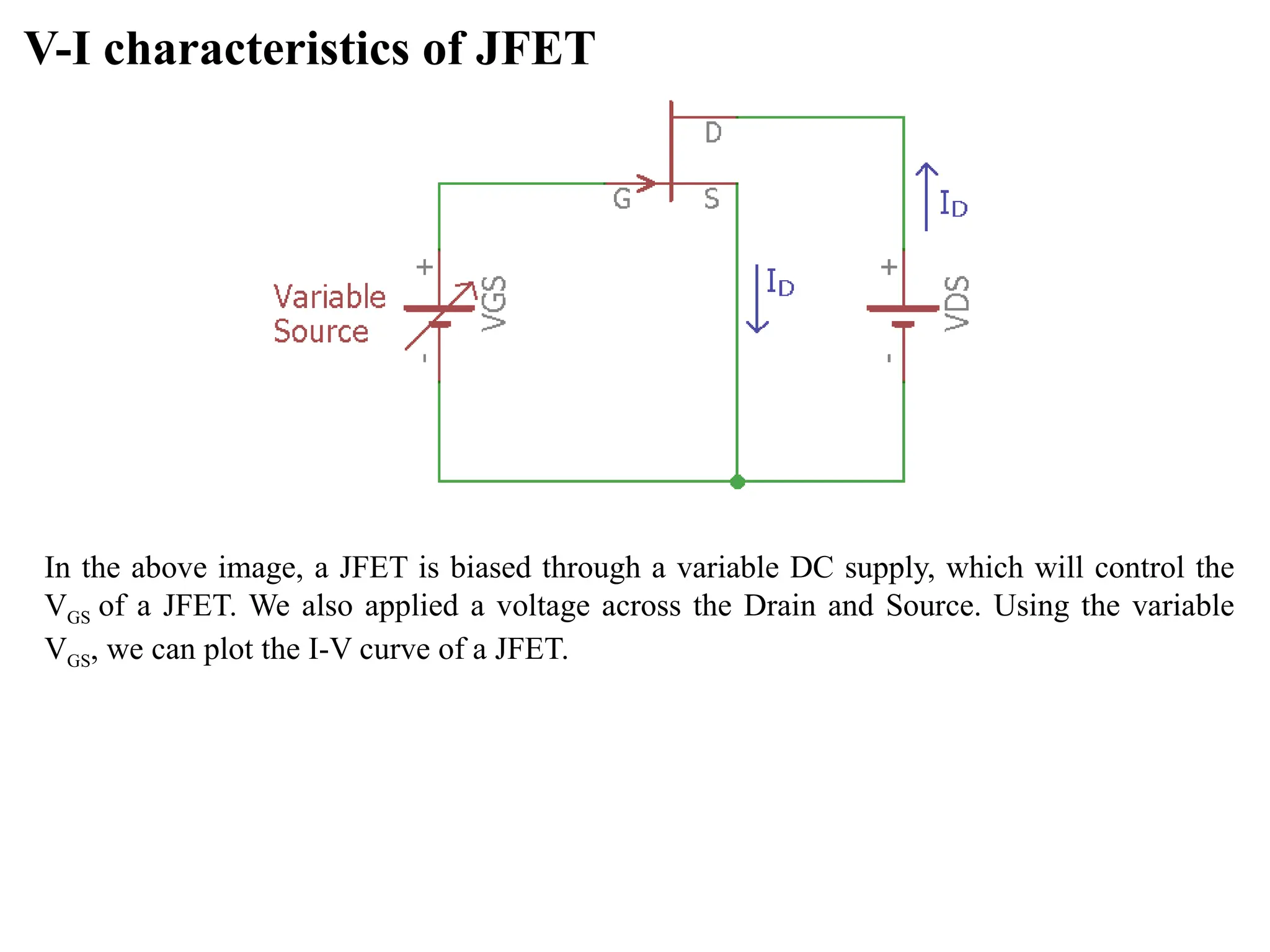
V-I characteristics ofJFET
In the above image, a JFET is biased through a variable DC supply, which will control the
VGS of a JFET. We also applied a voltage across the Drain and Source. Using the variable
VGS, we can plot the I-V curve of a JFET.
43.
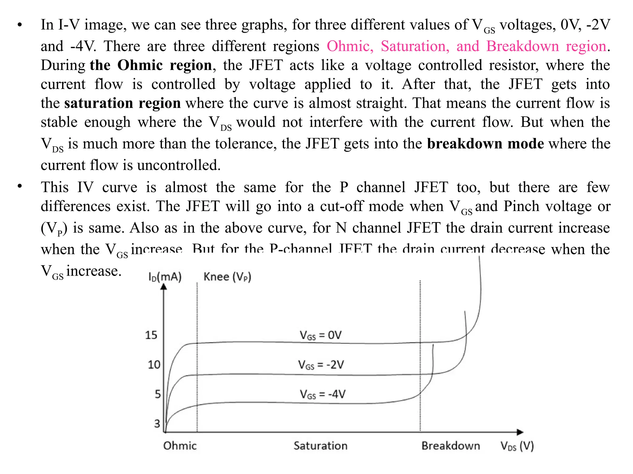
• In I-Vimage, we can see three graphs, for three different values of VGS voltages, 0V, -2V
and -4V. There are three different regions Ohmic, Saturation, and Breakdown region.
During the Ohmic region, the JFET acts like a voltage controlled resistor, where the
current flow is controlled by voltage applied to it. After that, the JFET gets into
the saturation region where the curve is almost straight. That means the current flow is
stable enough where the VDS would not interfere with the current flow. But when the
VDS is much more than the tolerance, the JFET gets into the breakdown mode where the
current flow is uncontrolled.
• This IV curve is almost the same for the P channel JFET too, but there are few
differences exist. The JFET will go into a cut-off mode when VGS and Pinch voltage or
(VP) is same. Also as in the above curve, for N channel JFET the drain current increase
when the VGS increase. But for the P-channel JFET the drain current decrease when the
VGS increase.
44.
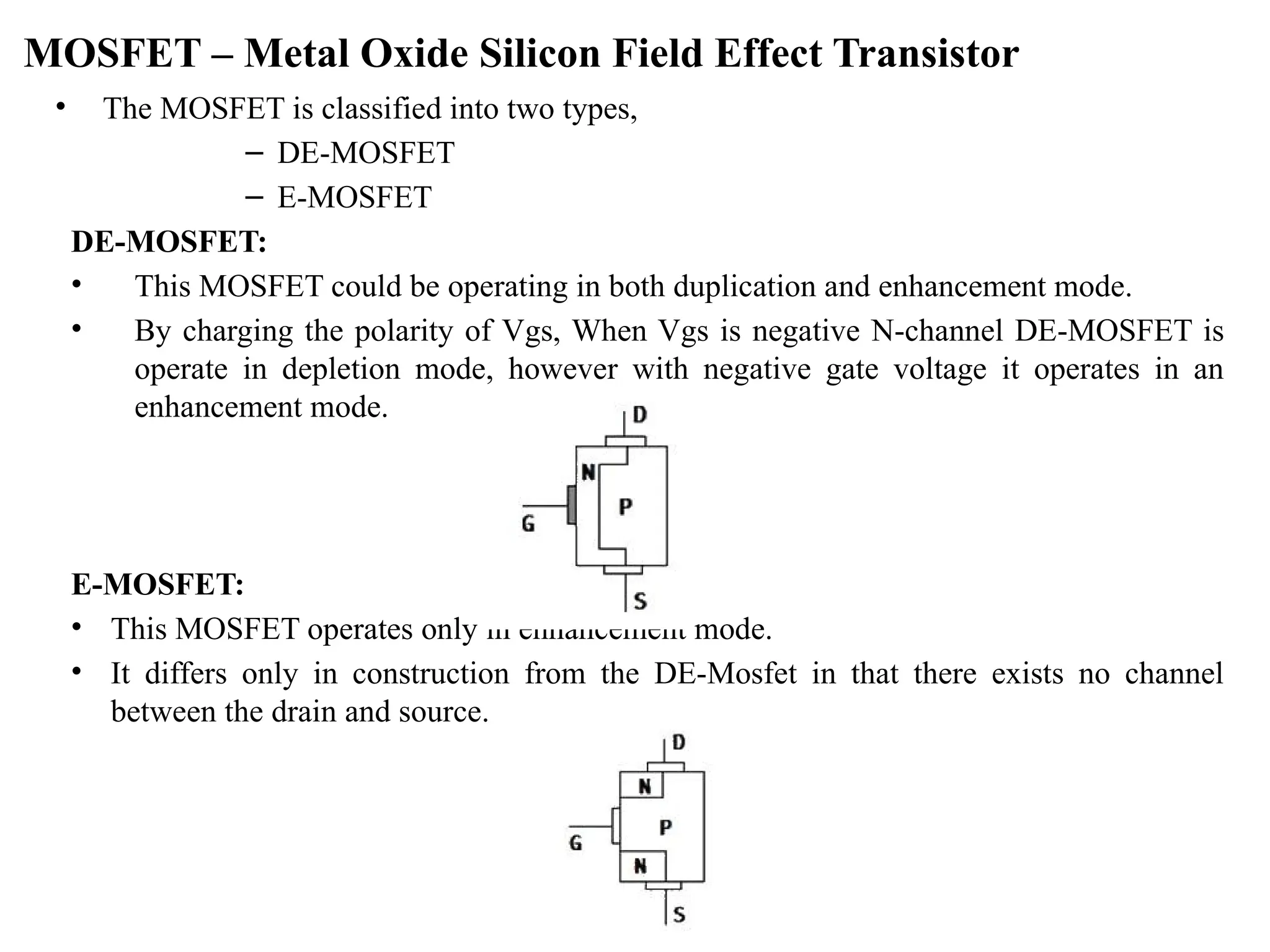
MOSFET – MetalOxide Silicon Field Effect Transistor
• The MOSFET is classified into two types,
– DE-MOSFET
– E-MOSFET
DE-MOSFET:
• This MOSFET could be operating in both duplication and enhancement mode.
• By charging the polarity of Vgs, When Vgs is negative N-channel DE-MOSFET is
operate in depletion mode, however with negative gate voltage it operates in an
enhancement mode.
E-MOSFET:
• This MOSFET operates only in enhancement mode.
• It differs only in construction from the DE-Mosfet in that there exists no channel
between the drain and source.
45.
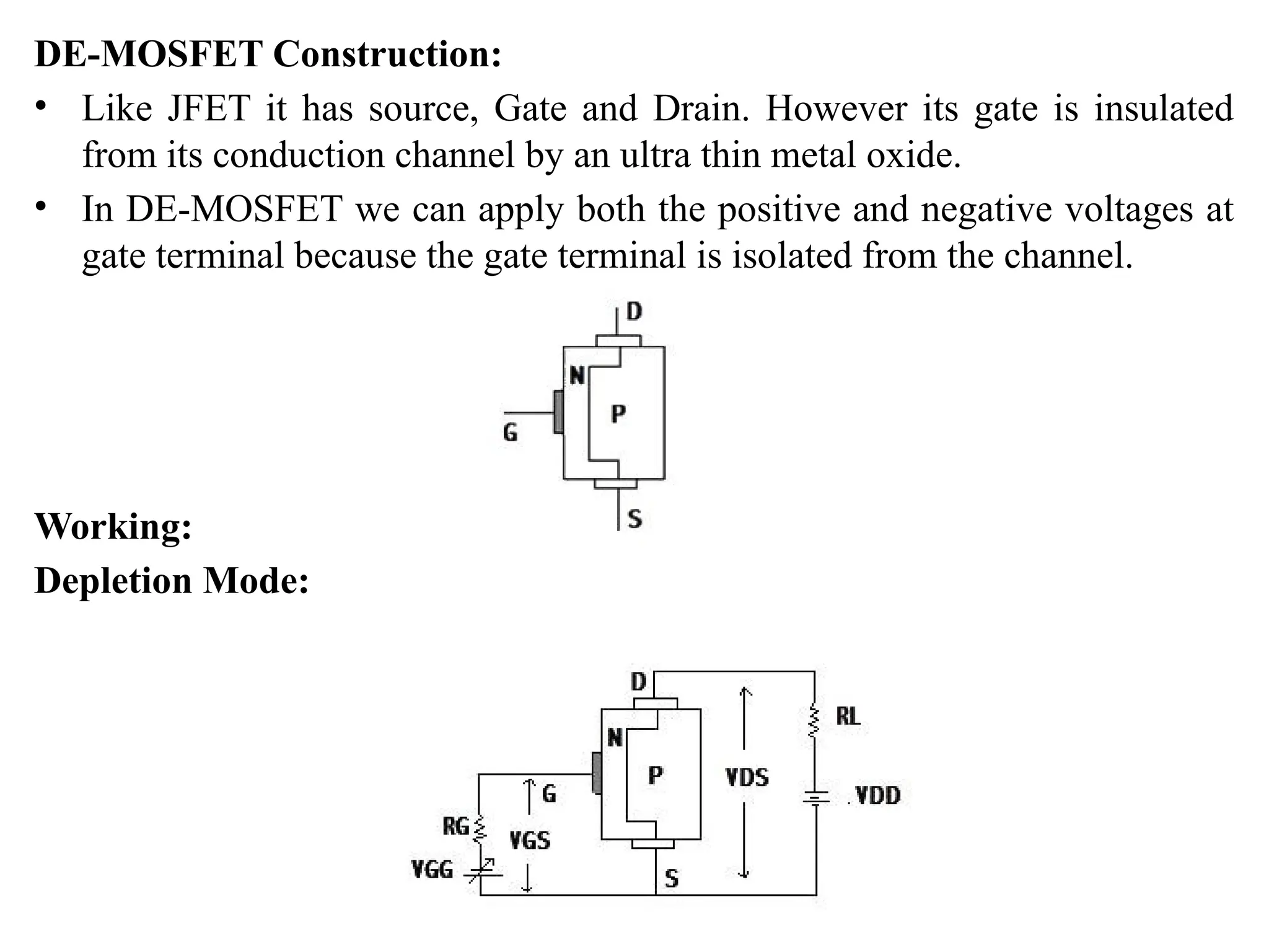
DE-MOSFET Construction:
• LikeJFET it has source, Gate and Drain. However its gate is insulated
from its conduction channel by an ultra thin metal oxide.
• In DE-MOSFET we can apply both the positive and negative voltages at
gate terminal because the gate terminal is isolated from the channel.
Working:
Depletion Mode:
46.
• When Vgs=0electrons can flow freely from source to drain through the conduction
channel, when a negative voltage is applied at gate terminal, it depletes the N-
channel and its electron by inducing positive charge in it.
• When we apply the negative voltage on the gate, the electron reduction take place in
channel which increase the conduction.
• In fact too much negative gate voltage cutoff the channel, thus with negative gate
voltage a DE-MOSFET behaves like a JFET, for this reason negative gate operation
of DE-MOSFET is called depletion mode operation.
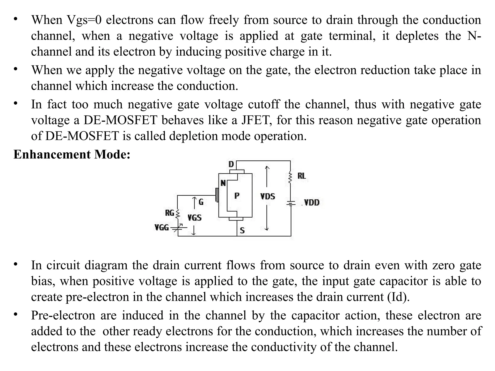
Enhancement Mode:
• In circuit diagram the drain current flows from source to drain even with zero gate
bias, when positive voltage is applied to the gate, the input gate capacitor is able to
create pre-electron in the channel which increases the drain current (Id).
• Pre-electron are induced in the channel by the capacitor action, these electron are
added to the other ready electrons for the conduction, which increases the number of
electrons and these electrons increase the conductivity of the channel.
47.
• As positivegate voltage increases the number of induced electrons
is increased which increase the conductivity of the channel from
source to drain, this way the current is also increased.
• The positive gate operation of the DE-MOSFET is known as
enhancement mode.
Application of MOSFET:
• As input amplifier in oscilloscope voltmeter, and other measuring
and testing equipment because they have high input resistance.
• It is used in logic circuits for fast switching
• It is also used in TV receiver.
• It is used in computer circuits.
• In high frequency amplifiers.
48.
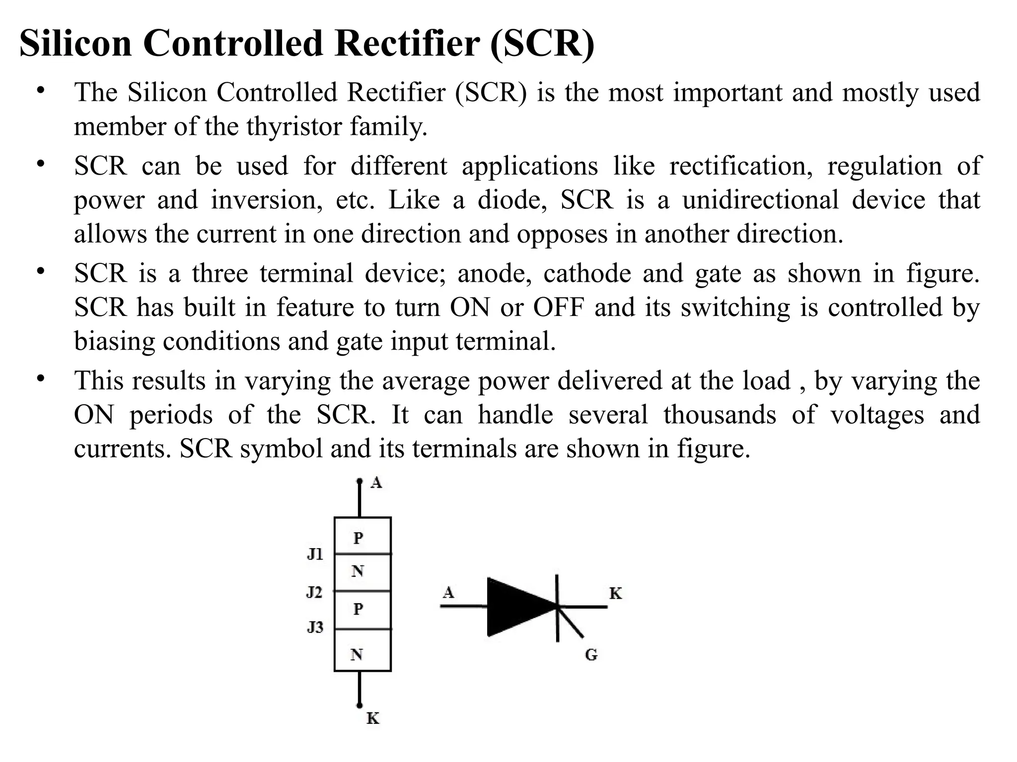
Silicon Controlled Rectifier(SCR)
• The Silicon Controlled Rectifier (SCR) is the most important and mostly used
member of the thyristor family.
• SCR can be used for different applications like rectification, regulation of
power and inversion, etc. Like a diode, SCR is a unidirectional device that
allows the current in one direction and opposes in another direction.
• SCR is a three terminal device; anode, cathode and gate as shown in figure.
SCR has built in feature to turn ON or OFF and its switching is controlled by
biasing conditions and gate input terminal.
• This results in varying the average power delivered at the load , by varying the
ON periods of the SCR. It can handle several thousands of voltages and
currents. SCR symbol and its terminals are shown in figure.
49.
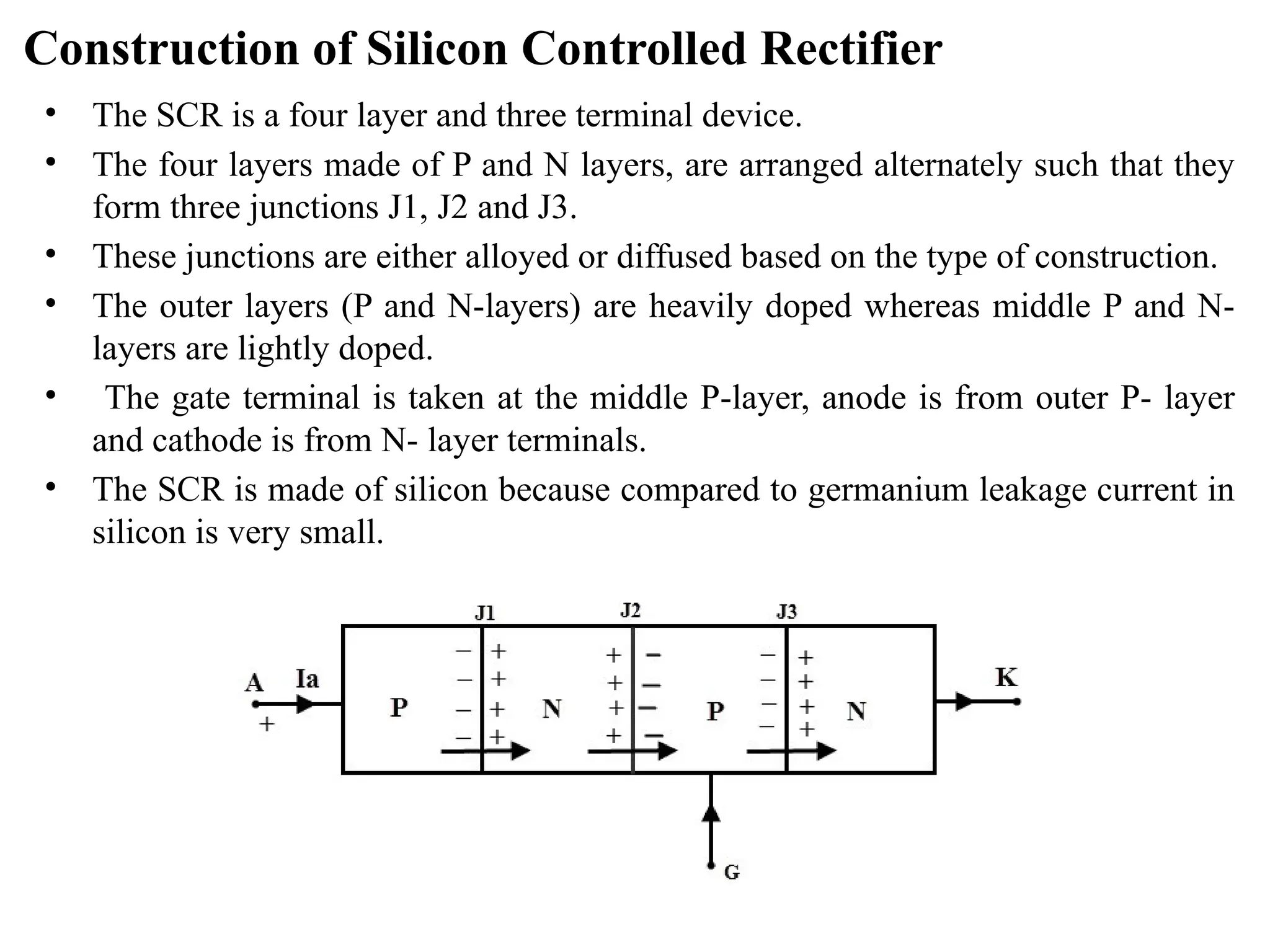
Construction of SiliconControlled Rectifier
• The SCR is a four layer and three terminal device.
• The four layers made of P and N layers, are arranged alternately such that they
form three junctions J1, J2 and J3.
• These junctions are either alloyed or diffused based on the type of construction.
• The outer layers (P and N-layers) are heavily doped whereas middle P and N-
layers are lightly doped.
• The gate terminal is taken at the middle P-layer, anode is from outer P- layer
and cathode is from N- layer terminals.
• The SCR is made of silicon because compared to germanium leakage current in
silicon is very small.
50.
Working or Modesof Operation of SCR
• Depending on the biasing given to the SCR, the operation of SCR is divided into three
modes. They are
• Forward blocking Mode
• Forward Conduction Mode and
• Reverse Blocking Mode
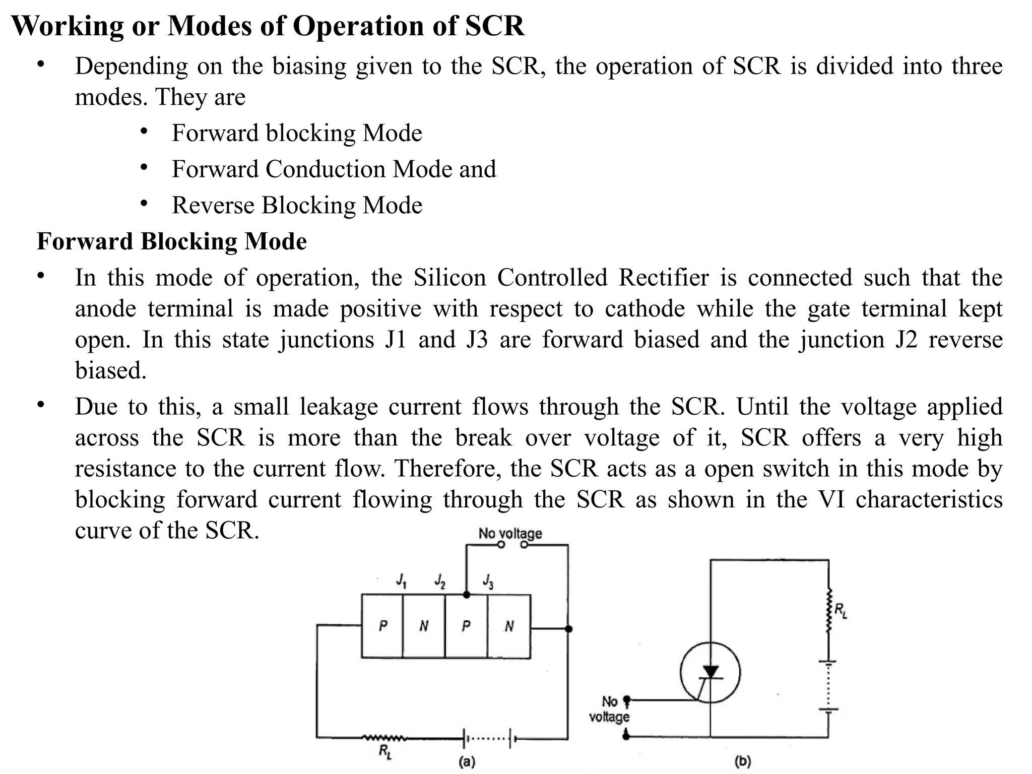
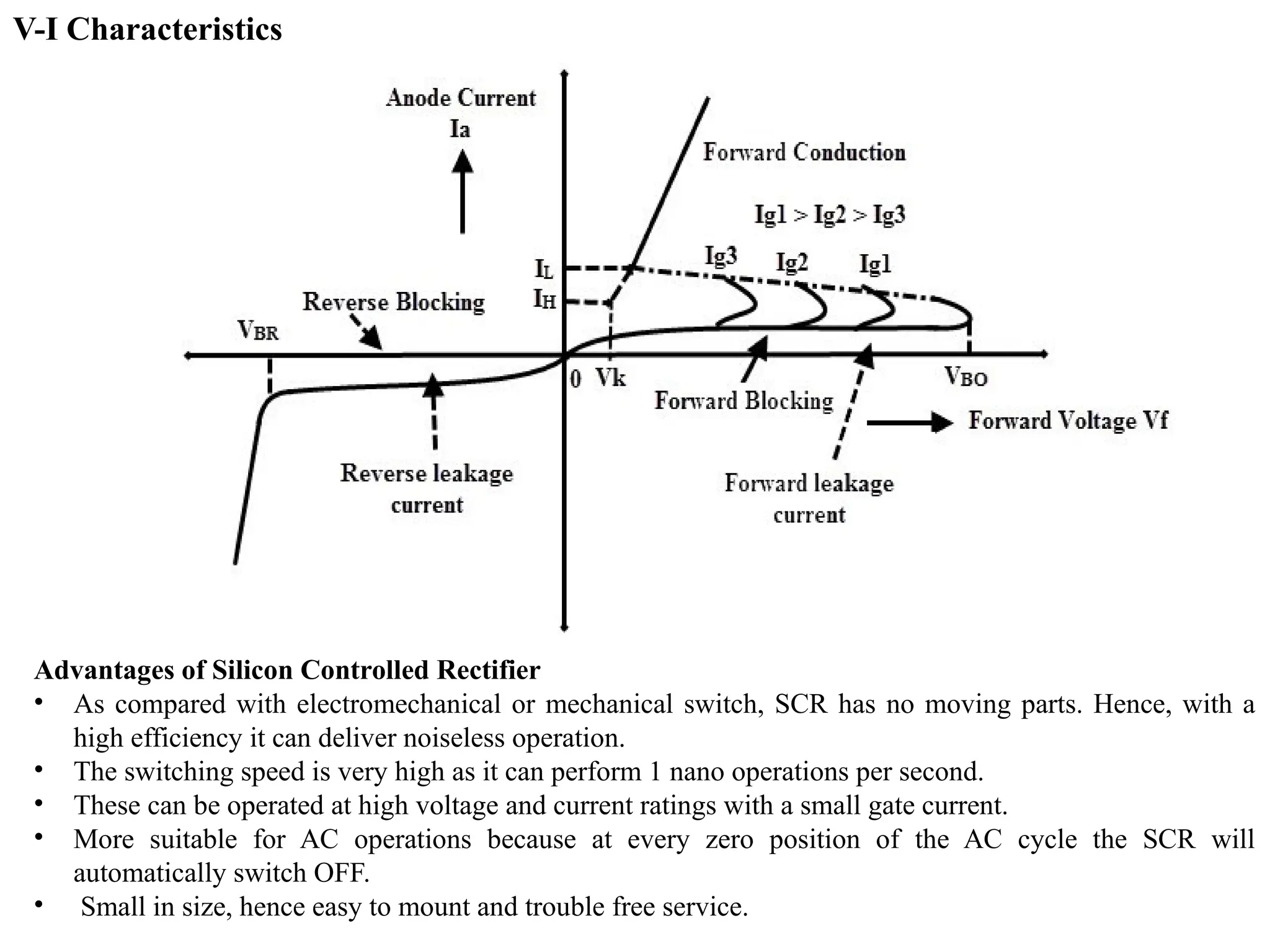
Forward Blocking Mode
• In this mode of operation, the Silicon Controlled Rectifier is connected such that the
anode terminal is made positive with respect to cathode while the gate terminal kept
open. In this state junctions J1 and J3 are forward biased and the junction J2 reverse
biased.
• Due to this, a small leakage current flows through the SCR. Until the voltage applied
across the SCR is more than the break over voltage of it, SCR offers a very high
resistance to the current flow. Therefore, the SCR acts as a open switch in this mode by
blocking forward current flowing through the SCR as shown in the VI characteristics
curve of the SCR.
51.
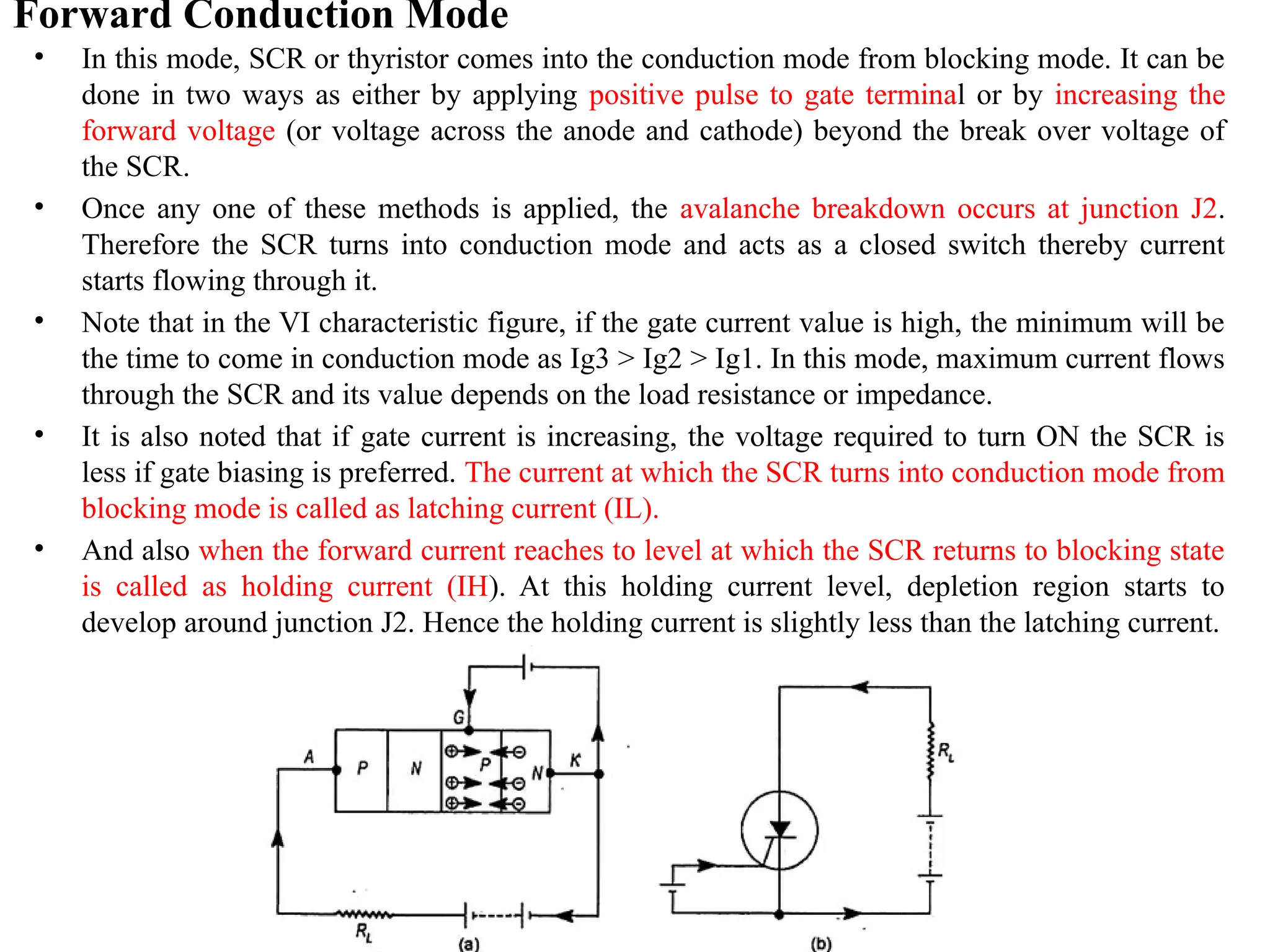
Forward Conduction Mode
•In this mode, SCR or thyristor comes into the conduction mode from blocking mode. It can be
done in two ways as either by applying positive pulse to gate terminal or by increasing the
forward voltage (or voltage across the anode and cathode) beyond the break over voltage of
the SCR.
• Once any one of these methods is applied, the avalanche breakdown occurs at junction J2.
Therefore the SCR turns into conduction mode and acts as a closed switch thereby current
starts flowing through it.
• Note that in the VI characteristic figure, if the gate current value is high, the minimum will be
the time to come in conduction mode as Ig3 > Ig2 > Ig1. In this mode, maximum current flows
through the SCR and its value depends on the load resistance or impedance.
• It is also noted that if gate current is increasing, the voltage required to turn ON the SCR is
less if gate biasing is preferred. The current at which the SCR turns into conduction mode from
blocking mode is called as latching current (IL).
• And also when the forward current reaches to level at which the SCR returns to blocking state
is called as holding current (IH). At this holding current level, depletion region starts to
develop around junction J2. Hence the holding current is slightly less than the latching current.
52.
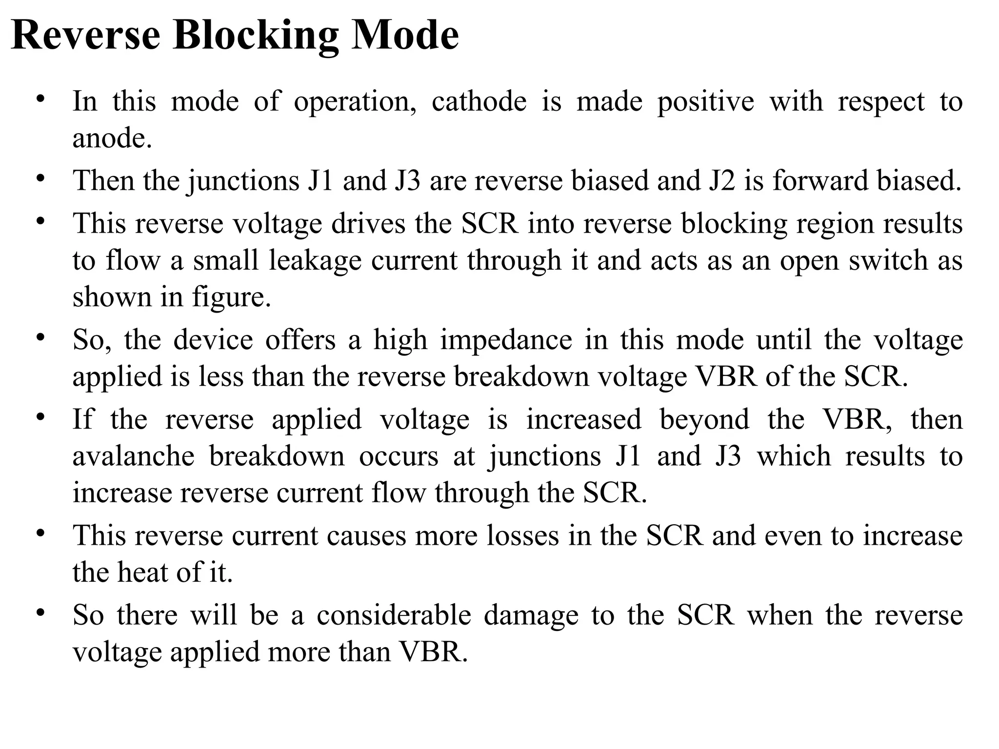
Reverse Blocking Mode
•In this mode of operation, cathode is made positive with respect to
anode.
• Then the junctions J1 and J3 are reverse biased and J2 is forward biased.
• This reverse voltage drives the SCR into reverse blocking region results
to flow a small leakage current through it and acts as an open switch as
shown in figure.
• So, the device offers a high impedance in this mode until the voltage
applied is less than the reverse breakdown voltage VBR of the SCR.
• If the reverse applied voltage is increased beyond the VBR, then
avalanche breakdown occurs at junctions J1 and J3 which results to
increase reverse current flow through the SCR.
• This reverse current causes more losses in the SCR and even to increase
the heat of it.
• So there will be a considerable damage to the SCR when the reverse
voltage applied more than VBR.
53.
V-I Characteristics
Advantages ofSilicon Controlled Rectifier
• As compared with electromechanical or mechanical switch, SCR has no moving parts. Hence, with a
high efficiency it can deliver noiseless operation.
• The switching speed is very high as it can perform 1 nano operations per second.
• These can be operated at high voltage and current ratings with a small gate current.
• More suitable for AC operations because at every zero position of the AC cycle the SCR will
automatically switch OFF.
• Small in size, hence easy to mount and trouble free service.
54.
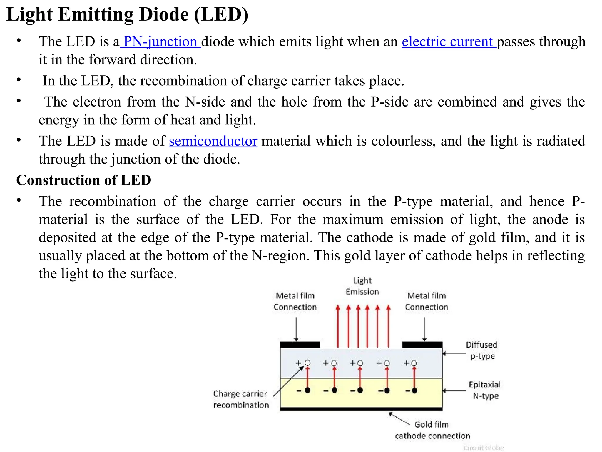
Light Emitting Diode(LED)
• The LED is a PN-junction diode which emits light when an electric current passes through
it in the forward direction.
• In the LED, the recombination of charge carrier takes place.
• The electron from the N-side and the hole from the P-side are combined and gives the
energy in the form of heat and light.
• The LED is made of semiconductor material which is colourless, and the light is radiated
through the junction of the diode.
Construction of LED
• The recombination of the charge carrier occurs in the P-type material, and hence P-
material is the surface of the LED. For the maximum emission of light, the anode is
deposited at the edge of the P-type material. The cathode is made of gold film, and it is
usually placed at the bottom of the N-region. This gold layer of cathode helps in reflecting
the light to the surface.
55.
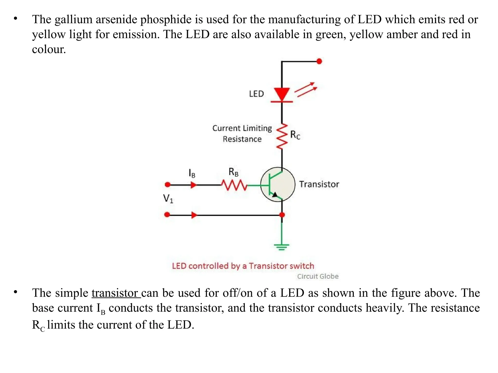
• The galliumarsenide phosphide is used for the manufacturing of LED which emits red or
yellow light for emission. The LED are also available in green, yellow amber and red in
colour.
• The simple transistor can be used for off/on of a LED as shown in the figure above. The
base current IB conducts the transistor, and the transistor conducts heavily. The resistance
RC limits the current of the LED.
56.
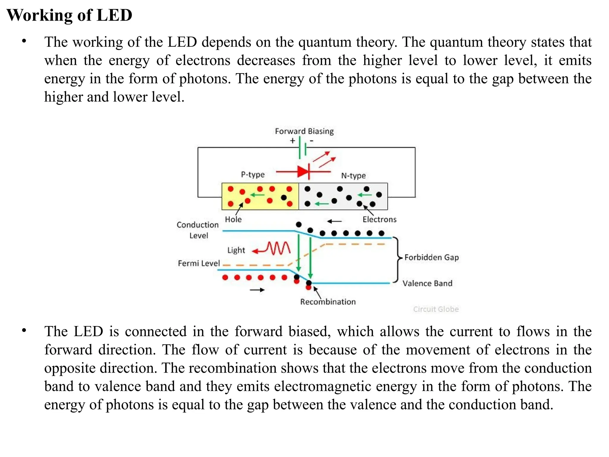
Working of LED
•The working of the LED depends on the quantum theory. The quantum theory states that
when the energy of electrons decreases from the higher level to lower level, it emits
energy in the form of photons. The energy of the photons is equal to the gap between the
higher and lower level.
• The LED is connected in the forward biased, which allows the current to flows in the
forward direction. The flow of current is because of the movement of electrons in the
opposite direction. The recombination shows that the electrons move from the conduction
band to valence band and they emits electromagnetic energy in the form of photons. The
energy of photons is equal to the gap between the valence and the conduction band.
57.
Advantages of LED
•The LED are smaller in sizes, and they can be stacked together
to form numeric and alphanumeric display in the high-density
matrix.
• The intensity of the light output of the LED depends on the
current flows through it. The intensity of their light can be
controlled smoothly.
• The LED are available which emits light in the different colours
like red, yellow, green and amber.
• The on and off time or switching time of the LED is less than of
1 nanoseconds. Because of this, the LED are used for the
dynamic operation.
Disadvantages of LED
• The LED consume more power as compared to LCD, and their
cost is high. Also, it is not used for making the large display.
58.
Uninterruptible Power Supply(UPS)
• An Uninterruptible Power Supply (UPS) is defined as a piece of
electrical equipment which can be used as an immediate power source to
the connected load when there is any failure in the main input power
source.
• When compared to other immediate power supply system, UPS have the
advantage of immediate protection against the input power interruptions.
• It has very short on-battery run time; however this time is enough to
safely shut down the connected apparatus (computers,
telecommunication equipment etc) or to switch on a standby power
source.
• UPS can be used as a protective device for some hardware which can
cause serious damage or loss with a sudden power disruption.
• Uninterruptible power source, Battery backup and Flywheel back up are
the other names often used for UPS.
• The available size of UPS units ranges from 200 VA which is used for a
solo computer to several large units up to 46 MVA.
59.
Types of UPS
•Generally, the UPS system is categorized into On-line UPS, Off- line UPS and
Line interactive UPS.
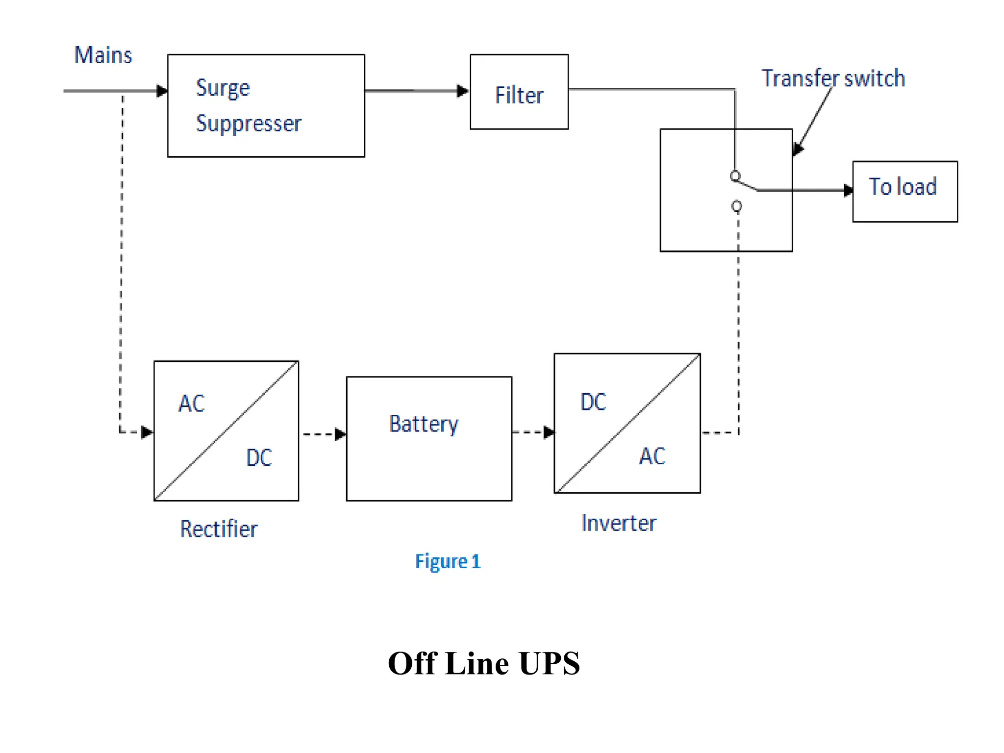
Off-line UPS
• This UPS is also called as Standby UPS system which can give only the most basic
features.
• Here, the primary source is the filtered AC mains (shown in solid path in figure 1).
• When the power breakage occurs, the transfer switch will select the backup source
(shown in dashed path in figure 1).
• Thus we can clearly see that the stand by system will start working only when
there is any failure in mains.
• In this system, the AC voltage is first rectified and stored in the storage battery
connected to the rectifier.
• When power breakage occurs, this DC voltage is converted to AC voltage by
means of a power inverter, and is transferred to the load connected to it.
• This is the least expensive UPS system and it provides surge protection in addition
to back up. The transfer time can be about 25 milliseconds which can be related to
the time taken by the UPS system to detect the utility voltage that is lost. The
block diagram is shown below
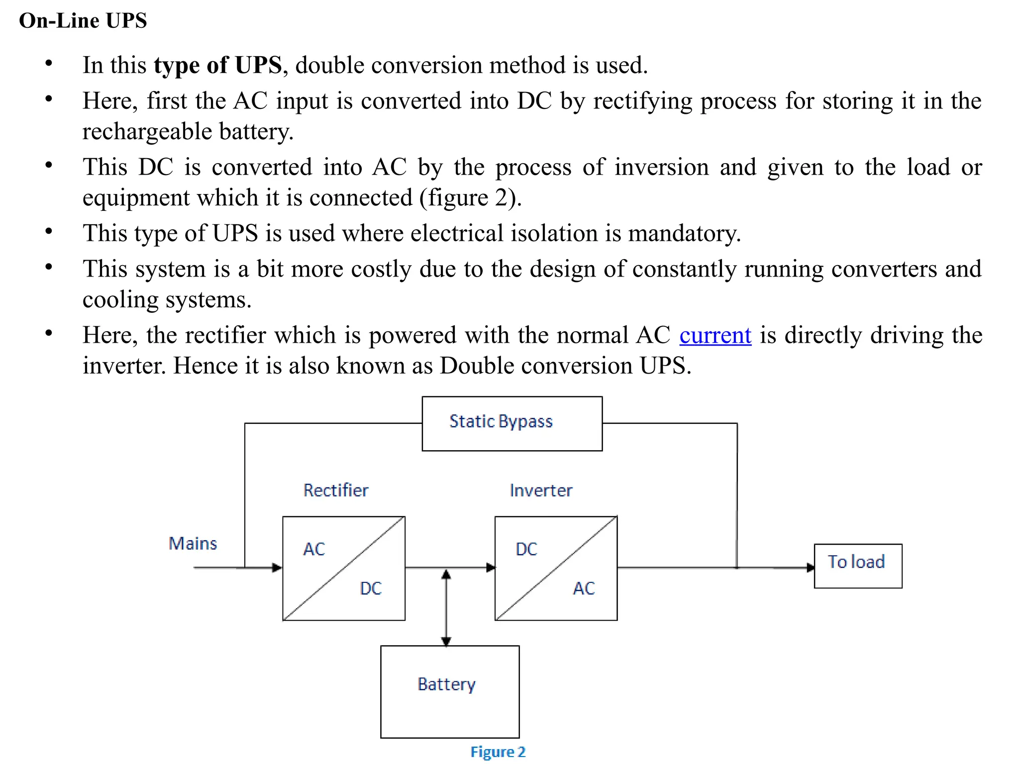
On-Line UPS
• Inthis type of UPS, double conversion method is used.
• Here, first the AC input is converted into DC by rectifying process for storing it in the
rechargeable battery.
• This DC is converted into AC by the process of inversion and given to the load or
equipment which it is connected (figure 2).
• This type of UPS is used where electrical isolation is mandatory.
• This system is a bit more costly due to the design of constantly running converters and
cooling systems.
• Here, the rectifier which is powered with the normal AC current is directly driving the
inverter. Hence it is also known as Double conversion UPS.
62.
• When thereis any power failure, the rectifier have no role in the circuit and
the steady power stored in the batteries which is connected to the inverter is
given to the load by means of transfer switch.
• Once the power is restored, the rectifier begins to charge the batteries.
• To prevent the batteries from overheating due to the high power rectifier, the
charging current is limited.
• During a main power breakdown, this UPS system operates with zero
transfer time.
• The reason is that the backup source acts as a primary source and not the
main AC input.
• But the presence of inrush current and large load step current can result in a
transfer time of about 4-6 milliseconds in this system.
UPS Applications
• Data Centers
• Industries
• Telecommunications
• Hospitals
• Banks and insurance
• Some special projects (events)
63.
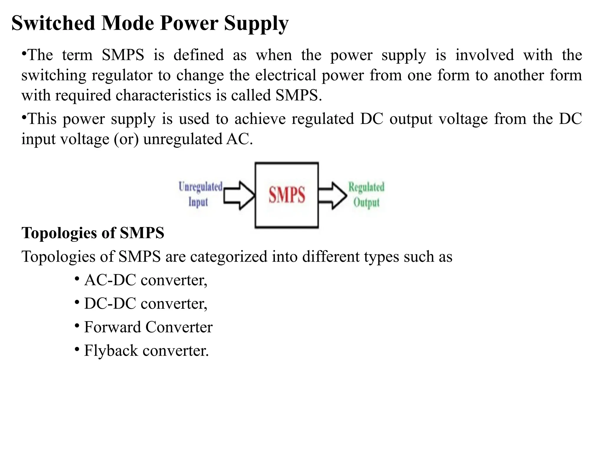
Switched Mode PowerSupply
•The term SMPS is defined as when the power supply is involved with the
switching regulator to change the electrical power from one form to another form
with required characteristics is called SMPS.
•This power supply is used to achieve regulated DC output voltage from the DC
input voltage (or) unregulated AC.
Topologies of SMPS
Topologies of SMPS are categorized into different types such as
• AC-DC converter,
• DC-DC converter,
• Forward Converter
• Flyback converter.
64.
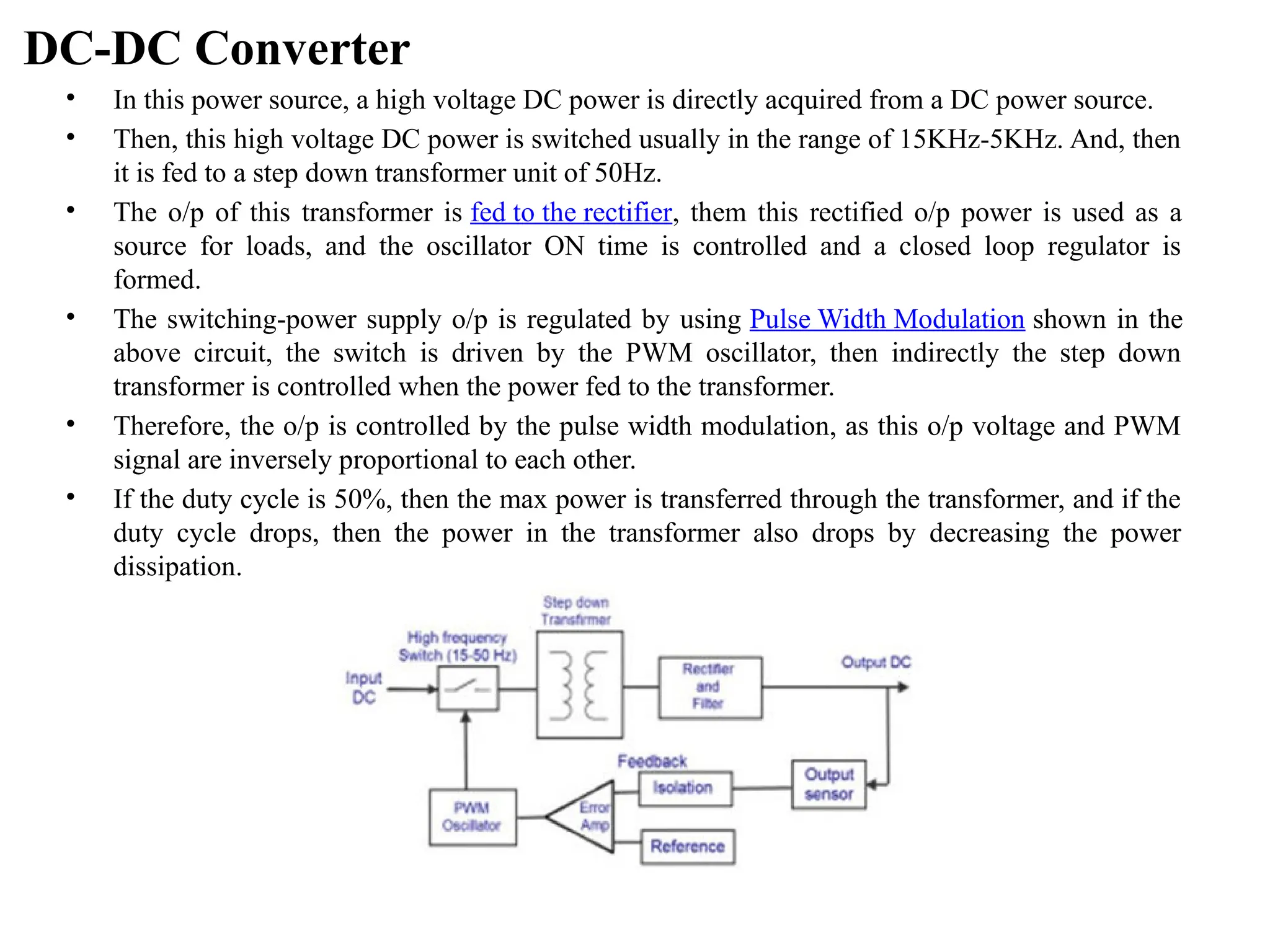
DC-DC Converter
• Inthis power source, a high voltage DC power is directly acquired from a DC power source.
• Then, this high voltage DC power is switched usually in the range of 15KHz-5KHz. And, then
it is fed to a step down transformer unit of 50Hz.
• The o/p of this transformer is fed to the rectifier, them this rectified o/p power is used as a
source for loads, and the oscillator ON time is controlled and a closed loop regulator is
formed.
• The switching-power supply o/p is regulated by using Pulse Width Modulation shown in the
above circuit, the switch is driven by the PWM oscillator, then indirectly the step down
transformer is controlled when the power fed to the transformer.
• Therefore, the o/p is controlled by the pulse width modulation, as this o/p voltage and PWM
signal are inversely proportional to each other.
• If the duty cycle is 50%, then the max power is transferred through the transformer, and if the
duty cycle drops, then the power in the transformer also drops by decreasing the power
dissipation.
65.
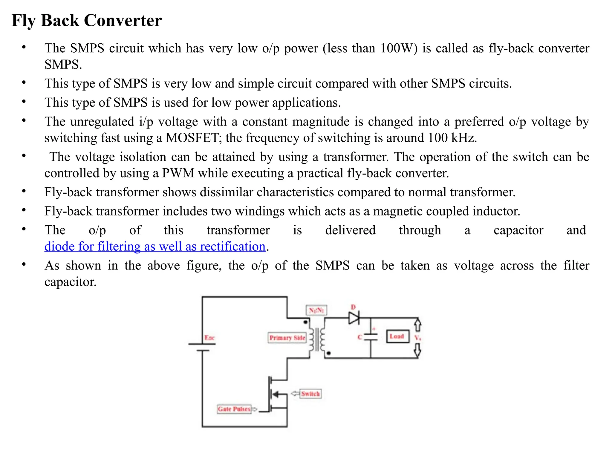
Fly Back Converter
•The SMPS circuit which has very low o/p power (less than 100W) is called as fly-back converter
SMPS.
• This type of SMPS is very low and simple circuit compared with other SMPS circuits.
• This type of SMPS is used for low power applications.
• The unregulated i/p voltage with a constant magnitude is changed into a preferred o/p voltage by
switching fast using a MOSFET; the frequency of switching is around 100 kHz.
• The voltage isolation can be attained by using a transformer. The operation of the switch can be
controlled by using a PWM while executing a practical fly-back converter.
• Fly-back transformer shows dissimilar characteristics compared to normal transformer.
• Fly-back transformer includes two windings which acts as a magnetic coupled inductor.
• The o/p of this transformer is delivered through a capacitor and
diode for filtering as well as rectification.
• As shown in the above figure, the o/p of the SMPS can be taken as voltage across the filter
capacitor.