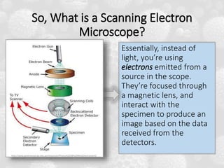
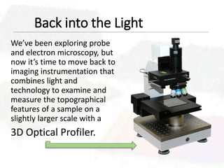
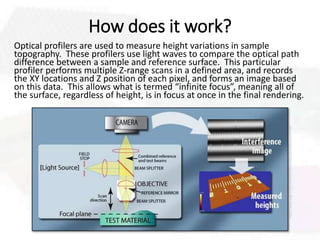
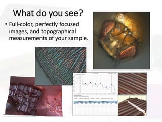
Getting a Closer Look:
An Introduction to
Nanotechnology Microscopy
By Kristina R. Boberg, NVCC
Image: http://jshs-tn.utk.edu/files/2012/10/Eye.jpg
Why do we use Microscopes?
• Sometimes we want to see
structures, surface details,
or even movement that
would be invisible to the
unaided eye.
• When dissecting, or
looking at a small sample,
we might just want a
magnified view.
• Or we want to see
specimens and organisms
at the tissue, cell, or
molecular level.
http://micro-scopic.tumblr.com/post/5551291228/anabaena
Scoping out the Competition
Until now, you’ve mostly
been using this type of
microscope,
but, as great as this scope
is, it has limitations. Now
you will learn about two
more types of microscopes
that will expand your
horizons, and allow you to
see beyond what light can
show you!
http://www.microscope.com
It’s all about
Resolution
Theoretically, an imaging
source (like a microscope)
should be able to resolve an
object the size of half the
wavelength of the imaging
energy.
So, if the object that you are
observing is smaller than half
the wavelength that you are
using, you won’t be able to
accurately resolve your
sample.
Structures that are close
together or that overlap
cannot resolve unless
the wavelength is short
enough.
http://www.ammrf.org.au/myscope/images/tem/resolution-wavelength.png
Will it Resolve?
http://www.nobelprize.org/educational/physics/microscopes/powerline/images/pl.gif
Move Away from the Light!
Light Microscope
• Wavelengths of Visible
light vary from 400-
700nm
• Light diffraction limits
resolution to 200-250nm
• Magnification limited to
around 1500x
Electron Microscope
• The wavelength of
electrons in an SEM is
5keV, or 0.017nm
• Resolution clarity to 1nm
• Magnification up to
500,000x
Versus
Essentially, instead of
light, you’re using
electrons emitted from a
source in the scope.
They’re focused through
a magnetic lens, and
interact with the
specimen to produce an
image based on the data
received from the
detectors.
So, What is a Scanning Electron
Microscope?
http://www.greenwood.wa.edu.au/resources/Physics%203B%20WestOne/content/
004_em_fields_force/images/pic066.jpg
How it WorksThe primary, or incident
beam scans the sample.
Some electrons “bounce”
off of the atoms in the
sample: those are
Backscattered electrons.
Some electrons are knocked
out of their energy levels by
the incident beam, and
these are Secondary
electrons—these are the
primary sources if specimen
information.
When a new electron jumps
energy levels to fill the hole
left by the incident beam,
energy is released as an X-
ray emission. http://www.ammrf.org.au/myscope/images/sem/volumes08.png
Surface of
Sample
What Can I Scan?
Since specimens are imaged in a
high-vacuum environment, there
are guidelines for what can be
scanned:
• The specimen has to be desiccated or
frozen (for cryogenic scanning).
• The specimen can not break apart or
outgas in the vacuum column.
• Ideally, it has to be conductive and
grounded (can be coated with a thin
layer of gold).
• It has to fit on the sample stub, and be
able to be mounted securely.
• Biological samples must be chemically
fixed, dried, and coated.
http://www.tedpella.com/SEMmod_html/16690.jpg
http://upload.wikimedia.org
http://isbbio1.pbworks.com/f/sem_8Group2.gif
This is What You Get
Large, clear images with
incredible detail.
K.Boberg,NVCC
K.Boberg,NVCC
But what if you want to look at something
that is even smaller, and perhaps still alive, or
is in liquid? Bacteria, living cells, proteins…
even DNA, perhaps?
(Sounds cool, right?
It is.)
You could use one
of these.
It’s an Atomic
Force Microscope.
What is Atomic Force Microscopy?
• AFM uses a physical probe to scan the sample,
instead of light or an electron beam.
• Nanoscale resolution—bonds between atoms
have been visualized on AFM, along with
viruses, DNA, and proteins.
• Samples don’t need to be in a vacuum, and do
not need to be conductive or desiccated
• Resolution more than 1000 times better than
the optical diffraction limit.
How does it Work?
A cantilever tip is put in contact with a
surface. An ionic repulsive force from
the surface, when applied to the tip,
bends the cantilever upwards.
The amount of bending is measured
by a laser spot reflected on to a
detector, and can be used to calculate
the ionic force.
Scanning the tip across the surface
allows the vertical movement of the
tip to follow the surface profile and is
recorded as the surface topography.
Here is a short video on how it works.
http://www.home.agilent.com/upload/cmc_
upload/ck/zz-other/images/AFM_schematic.gif
What You Can See*
* but only with optimum conditions and materials,
minimal vibration, a new cantilever, and with well-
prepared samples.
A living cell, Gold
Colloid, and DNA are
shown here.
Samples like these
can be viewed with
clarity and ease on
an AFM…
Back into the Light
We’ve been exploring probe
and electron microscopy, but
now it’s time to move back to
imaging instrumentation that
combines light and
technology to examine and
measure the topographical
features of a sample on a
slightly larger scale with a
3D Optical Profiler.
Optical Metrology Using the 3-D
Optical Profiler
Used for micrometer-scale
characterization, since the
wavelengths of light are
the limiting factor.
Provides a 3-D rendering of
the surface, to measure
the topographical features
of your sample.
Great for quality assurance
and measurements.
http://cwitechsales.com/Precision_Metrology.html
How does it work?
Optical profilers are used to measure height variations in sample
topography. These profilers use light waves to compare the optical path
difference between a sample and reference surface. This particular
profiler performs multiple Z-range scans in a defined area, and records
the XY locations and Z position of each pixel, and forms an image based
on this data. This allows what is termed “infinite focus”, meaning all of
the surface, regardless of height, is in focus at once in the final rendering.
http://www.zygo.com/?/met/profilers/opticalprofilersabout.htm
What samples can you use?
You can use anything that will fit under the objective!
Wet, dry, living or inorganic—the 3D Optical Profiler can
image it.
Flatter items are
preferable, to get the
most surface area in one
image, but insects,
plants, bacterial cultures,
and inorganic samples
can be measured and
characterized in full-
color detail.
http://www.zeta-inst.com/products/true-color-3D-optical-profiler
What do you see?
• Full-color, perfectly focused
images, and topographical
measurements of your sample.
http://www.nanoscience.com/products/optical-profilometry/optical-metrology-platform/
With Great (Magnifying) Power…
comes great responsibility.
These imaging instruments are very powerful, but
require a very delicate touch, constant care,
meticulous sample preparation, and frequent
calibration, which can be time consuming and
costly. That is why they are not as common as the
microscopes normally found in a classroom.
However, when you do have access to them, they
are an invaluable source of information and
scientific data as nanotechnology becomes more
important in the world of science and technology.
Thank you!
Now that you have all of this new information,
think of ways the instruments described and
demonstrated today can be incorporated into
your studies here at NOVA, and how they might
influence your future.
If you have any further questions, contact:
• Dr. Ia Gomez at igomez@nvcc.edu, or
• Kristina Boberg at kboberg@nvcc.edu.
Microscopy and Nanotechnology
Resources
• https://www.jic.ac.uk/microscopy/scale.html
• https://www.jic.ac.uk/microscopy/intro_LM.html
• https://www.jic.ac.uk/microscopy/intro_EM.html
• http://home.nas.net/~dbc/cic_hamilton/emicro.html
• http://nanotechweb.org/
• http://nano4me.org
• http://www.understandingnano.com/resources.html
• http://www.nanosurf.com/?content=04&gclid=CN7E24SyvsACFVQV7Aod
M3wAMQ

SEM, AFM, and 3D Optical Profiler Introduction

  • 1.
    Getting a CloserLook: An Introduction to Nanotechnology Microscopy By Kristina R. Boberg, NVCC Image: http://jshs-tn.utk.edu/files/2012/10/Eye.jpg
  • 2.
    Why do weuse Microscopes? • Sometimes we want to see structures, surface details, or even movement that would be invisible to the unaided eye. • When dissecting, or looking at a small sample, we might just want a magnified view. • Or we want to see specimens and organisms at the tissue, cell, or molecular level. http://micro-scopic.tumblr.com/post/5551291228/anabaena
  • 3.
    Scoping out theCompetition Until now, you’ve mostly been using this type of microscope, but, as great as this scope is, it has limitations. Now you will learn about two more types of microscopes that will expand your horizons, and allow you to see beyond what light can show you! http://www.microscope.com
  • 4.
    It’s all about Resolution Theoretically,an imaging source (like a microscope) should be able to resolve an object the size of half the wavelength of the imaging energy. So, if the object that you are observing is smaller than half the wavelength that you are using, you won’t be able to accurately resolve your sample. Structures that are close together or that overlap cannot resolve unless the wavelength is short enough. http://www.ammrf.org.au/myscope/images/tem/resolution-wavelength.png
  • 5.
  • 6.
    Move Away fromthe Light! Light Microscope • Wavelengths of Visible light vary from 400- 700nm • Light diffraction limits resolution to 200-250nm • Magnification limited to around 1500x Electron Microscope • The wavelength of electrons in an SEM is 5keV, or 0.017nm • Resolution clarity to 1nm • Magnification up to 500,000x Versus
  • 7.
    Essentially, instead of light,you’re using electrons emitted from a source in the scope. They’re focused through a magnetic lens, and interact with the specimen to produce an image based on the data received from the detectors. So, What is a Scanning Electron Microscope? http://www.greenwood.wa.edu.au/resources/Physics%203B%20WestOne/content/ 004_em_fields_force/images/pic066.jpg
  • 8.
    How it WorksTheprimary, or incident beam scans the sample. Some electrons “bounce” off of the atoms in the sample: those are Backscattered electrons. Some electrons are knocked out of their energy levels by the incident beam, and these are Secondary electrons—these are the primary sources if specimen information. When a new electron jumps energy levels to fill the hole left by the incident beam, energy is released as an X- ray emission. http://www.ammrf.org.au/myscope/images/sem/volumes08.png Surface of Sample
  • 9.
    What Can IScan? Since specimens are imaged in a high-vacuum environment, there are guidelines for what can be scanned: • The specimen has to be desiccated or frozen (for cryogenic scanning). • The specimen can not break apart or outgas in the vacuum column. • Ideally, it has to be conductive and grounded (can be coated with a thin layer of gold). • It has to fit on the sample stub, and be able to be mounted securely. • Biological samples must be chemically fixed, dried, and coated. http://www.tedpella.com/SEMmod_html/16690.jpg http://upload.wikimedia.org http://isbbio1.pbworks.com/f/sem_8Group2.gif
  • 10.
    This is WhatYou Get Large, clear images with incredible detail. K.Boberg,NVCC K.Boberg,NVCC
  • 11.
    But what ifyou want to look at something that is even smaller, and perhaps still alive, or is in liquid? Bacteria, living cells, proteins… even DNA, perhaps? (Sounds cool, right? It is.) You could use one of these. It’s an Atomic Force Microscope.
  • 12.
    What is AtomicForce Microscopy? • AFM uses a physical probe to scan the sample, instead of light or an electron beam. • Nanoscale resolution—bonds between atoms have been visualized on AFM, along with viruses, DNA, and proteins. • Samples don’t need to be in a vacuum, and do not need to be conductive or desiccated • Resolution more than 1000 times better than the optical diffraction limit.
  • 13.
    How does itWork? A cantilever tip is put in contact with a surface. An ionic repulsive force from the surface, when applied to the tip, bends the cantilever upwards. The amount of bending is measured by a laser spot reflected on to a detector, and can be used to calculate the ionic force. Scanning the tip across the surface allows the vertical movement of the tip to follow the surface profile and is recorded as the surface topography. Here is a short video on how it works. http://www.home.agilent.com/upload/cmc_ upload/ck/zz-other/images/AFM_schematic.gif
  • 14.
    What You CanSee* * but only with optimum conditions and materials, minimal vibration, a new cantilever, and with well- prepared samples. A living cell, Gold Colloid, and DNA are shown here. Samples like these can be viewed with clarity and ease on an AFM…
  • 15.
    Back into theLight We’ve been exploring probe and electron microscopy, but now it’s time to move back to imaging instrumentation that combines light and technology to examine and measure the topographical features of a sample on a slightly larger scale with a 3D Optical Profiler.
  • 16.
    Optical Metrology Usingthe 3-D Optical Profiler Used for micrometer-scale characterization, since the wavelengths of light are the limiting factor. Provides a 3-D rendering of the surface, to measure the topographical features of your sample. Great for quality assurance and measurements. http://cwitechsales.com/Precision_Metrology.html
  • 17.
    How does itwork? Optical profilers are used to measure height variations in sample topography. These profilers use light waves to compare the optical path difference between a sample and reference surface. This particular profiler performs multiple Z-range scans in a defined area, and records the XY locations and Z position of each pixel, and forms an image based on this data. This allows what is termed “infinite focus”, meaning all of the surface, regardless of height, is in focus at once in the final rendering. http://www.zygo.com/?/met/profilers/opticalprofilersabout.htm
  • 18.
    What samples canyou use? You can use anything that will fit under the objective! Wet, dry, living or inorganic—the 3D Optical Profiler can image it. Flatter items are preferable, to get the most surface area in one image, but insects, plants, bacterial cultures, and inorganic samples can be measured and characterized in full- color detail. http://www.zeta-inst.com/products/true-color-3D-optical-profiler
  • 19.
    What do yousee? • Full-color, perfectly focused images, and topographical measurements of your sample. http://www.nanoscience.com/products/optical-profilometry/optical-metrology-platform/
  • 20.
    With Great (Magnifying)Power… comes great responsibility. These imaging instruments are very powerful, but require a very delicate touch, constant care, meticulous sample preparation, and frequent calibration, which can be time consuming and costly. That is why they are not as common as the microscopes normally found in a classroom. However, when you do have access to them, they are an invaluable source of information and scientific data as nanotechnology becomes more important in the world of science and technology.
  • 21.
    Thank you! Now thatyou have all of this new information, think of ways the instruments described and demonstrated today can be incorporated into your studies here at NOVA, and how they might influence your future. If you have any further questions, contact: • Dr. Ia Gomez at igomez@nvcc.edu, or • Kristina Boberg at kboberg@nvcc.edu.
  • 22.
    Microscopy and Nanotechnology Resources •https://www.jic.ac.uk/microscopy/scale.html • https://www.jic.ac.uk/microscopy/intro_LM.html • https://www.jic.ac.uk/microscopy/intro_EM.html • http://home.nas.net/~dbc/cic_hamilton/emicro.html • http://nanotechweb.org/ • http://nano4me.org • http://www.understandingnano.com/resources.html • http://www.nanosurf.com/?content=04&gclid=CN7E24SyvsACFVQV7Aod M3wAMQ