Downloaded 446 times


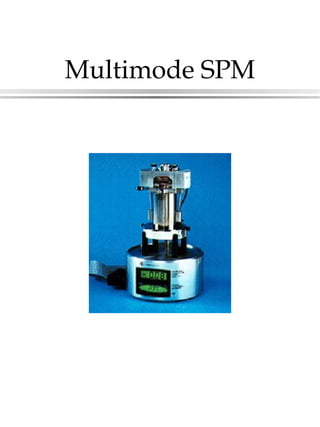
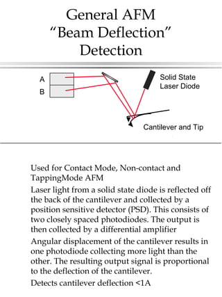
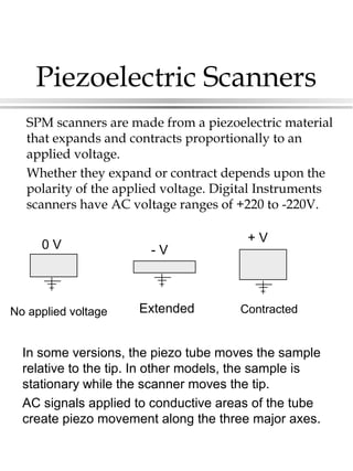


Atomic force microscopy (AFM) is a type of scanning probe microscopy that uses a sharp probe to scan over a sample surface. It operates by measuring the forces between the probe and sample using a laser beam and photodetector to measure the probe's deflection. There are three main imaging modes: contact mode, non-contact mode, and tapping mode. AFM provides topographic, mechanical, and other property information with nanoscale resolution and is widely used in materials science and biology.


