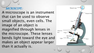
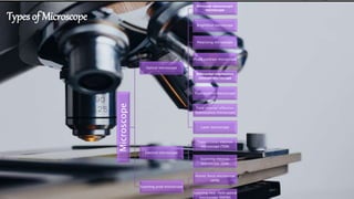
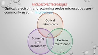
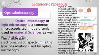
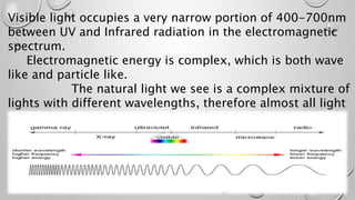
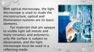
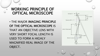
MICROSCOPY:
The science of Investigating small objects
Using such an instrument Is called microscopy.
The word "microscopy" comes from Greek
roots: mikros, small + skopeo, to view = to view small
(objects).
Microscopy is the technical field Of using
microscope to view objects and areas Of objects that
can’t be Seen with naked eye.In most materials the constituent grains are
of microscopic dimensions, having diameters that may
be on the order of microns (A micron sometimes called a
micrometer, is 10-6m) and their details must be
MICROSCOPE:
A microscope is an instrument
that can be used to observe
small objects, even cells. The
image of an object is
magnified through lenses in
the microscope. These lenses
bends light toward the eye and
makes an object appear larger
than it actually is.
Microscope
Optical microscope
Binocular stereoscopic
microscope
Brightfield microscope
Polarizing microscope
Phase contrast microscope
Differential interference
contrast microscope
Fluorescence microscope
Total internal reflection
fluorescence microscope
Laser microscope
Electron microscope
Transmission electron
microscope (TEM)
Scanning electron
microscope (SEM)
Scanning prob microscope
Atomic force microscope
(AFM)
Scanning near-field optical
microscope (SNOM)
Types of Microscope
MICROSCOPIC TECHNIQUES
Optical
microscopy
Electron
microscope
Scanning
prob
microscopy
Optical, electron, and scanning probe microscopes are
commonly used in microscopy.
MICROSCOPIC TECHNIQUES
Opticalmicroscopy
Figure 4.13 (a)
Polished and etched
grains as they might
appear when viewed
with an optical
microscope. (b) Section
taken through these
grains showing how the
etching characteristics
and resulting surface
texture vary from grain
to grain because of
differences in
crystallographic
orientation. (c)
Photomicrograph of a
polycrystalline brass
specimen. 60-
.
(Photomicrograph
courtesy of J. E. Burke,
General Electric Co.)
The visible part of
electromagnetic spectrum is the
type of radiation used by optical
microscopy.
Optical microscopy or
light microscopy is a common
microscopic technique oftenly
used in material Sciences as well
in life sciences.
Visible light occupies a very narrow portion of 400-700nm
between UV and Infrared radiation in the electromagnetic
spectrum.
Electromagnetic energy is complex, which is both wave
like and particle like.
The natural light we see is a complex mixture of
lights with different wavelengths, therefore almost all light
sources provide a mixture of wavelengths of light.
With optical microscopy, the light
microscope is used to study the
microstructure; optical and
illumination systems are its basic
elements.
. For materials that are opaque
to visible light (all metals and
many ceramics and polymers),
only the surface is subject to
observation, and the light
microscope must be used in a
reflecting mode.
• THE MAJOR IMAGING PRINCIPLE
OF THE OPTICAL MICROSCOPE IS
THAT AN OBJECTIVE LENS WITH
VERY SHORT FOCAL LENGTH IS
USED TO FORM A HIGHLY
MAGNIFIED REAL IMAGE OF THE
OBJECT.
WORKING PRINCIPLE OF
OPTICAL MICROSCOPE
SAMPLE PREPARATION
When preparing samples for microscopy, it is important
to produce something that is representative of the whole
specimen. It is not always possible to achieve this with a
single sample. Indeed, it is always good practice to mount
samples from a material under study in more than one
orientation. The variation in material properties will
affect how the preparation should be handled, for
example very soft or ductile materials may be difficult to
polish mechanically.
Cutting
•It important to be alert to the fact that preparation of a
specimen may change the microstructure of the material,
for example through heating, chemical attack, or
mechanical damage. The amount of damage depends on
the method by which the specimen is cut and the
material itself.
Cutting with abrasives may cause a large amount of
damage, whilst the use of a low-speed diamond saw can
Metal
working
Wood
working
Chemical-
mechanical
polishing
Flame
polishing
Vapour
polishing
Ultra-fine
abrasive
paste
polishing
Polishing
Polishing is the process of creating smooth and shiny
surface by rubbing it or using a chemical action leaving a
surface with a significant specular reflection.
The process of polishing with abrasive starts with coarse
ones and graduates to fine one.
Types
Etching
•Etching is used to reveal the
microstructure of the metal through
selective chemical attack. It also
removes the thin, highly deformed layer
introduced during grinding and
polishing.
•The rate of etching is affected by
crystallographic orientation, the phase
Electron microscopy (EM) is a technique for
obtaining high resolution images of material and non-
material (biological) specimens.
It is a versatile tool with a range of
methodologies to characterize the microstructural
features of a sample from 100pm to 100μm length
scales.
The high resolution of EM images results from the
use of electrons (which have very short wavelengths) as
the source of illuminating radiation. EM images provide
key information on the structural basis of materials.
Electron
Microscopy
TYPES OF ELECTRON MICROSCOPY
ElectronMicroscopy
Transmission Electron
Microscopy (TEM)
Bright Field (BF)
Dark Field (DF)
Electron Diffraction (ED)
Energy Filtered Transmission
Electron Microscopy (EFTEM)
High-Resolution Transmission
Electron Microscop (HRTEM)
Scanning Electron
Microscopy (SEM)
Bright Field (BF)
Dark Field (DF)
High-Angle Annular Dark
Field (HAADF)
TRANSMITTEDELECTRONMICROSCOPY TEM
The transmission electron microscope is a
very powerful tool for material science. A high energy
beam of electrons is shone through a very thin sample,
and the interactions between the electrons and the
atoms can be used to observe features such as the
crystal structure and features in the structure like
dislocations and grain boundaries. Chemical analysis
can also be performed. TEM can be used to study the
growth of layers, their composition and defects in
semiconductors. High resolution can be used to analyze
the quality, shape, size and density of quantum wells,
WORKING PRINCIPLE OF TEM
The TEM operates on the same
basic principles as the light
microscope but uses electrons
instead of light. Because the
wavelength of electrons is much
smaller than that of light, the
optimal resolution attainable for
TEM images is many orders of
magnitude better than that from a
light microscope. Thus, TEMs can
reveal the finest details of internal
SCANNING ELECTRONMICROSCOPE (SEM)
Scanning Electron Microscope is a type of Electron
microscope that produces image of a sample by scanning
it with a beam of electrons.
Magnifications ranging from 10 to in excess of
50,000 times are possible, as are also very great depths of
field.
WORKING PRINCIPLE OF SEM
Accelerated electrons in a SEM
carry significant amount of
kinetic energy, and this energy
is dissipated as a variety of
signals produce by electron-
sample interactions when the
incident electrons are
declarated in solid sample.
These signals include
secondary electrons that
TEMVS SEM
1. TEM is based on transmitted electrons while SEM is
based on scattered electrons.
2. TEM focuses on the internal composition whereas SEM
provides information about the sample‘s surface and
its composition.
Therefore TEM can show many characteristics of the
sample, such as morphology, crystalization, stress or
even magnetic domains. On the other hand, SEM shows
only the morphology of the sample.
3. TEM has much higher resolution than SEM.
4. TEM is used for imaging of dislocations, tiny
precipitates, grain boundaries and other defect structures
5. In TEM, pictures are shown on flourescent screen
whereas in SEM, picture is shown on monitor.
6. TEM provides a two-dimensional picture whereas SEM
also provides a three-dimensional picture.
Scanningprob
microscopy
Scanning prob microscopy SPM is the name of a group
of microscopy techniques in which a physical probe (tip)
scans the sample. The interaction between the probe and
the sample is measured as a function of their relative
position.
SPM techniques are very versatile, and many types of
measurement can be performed depending on the kind
of interaction between the probe and the specimen.
SPM techniques include Scanning Tunnelling
Microscopy (STM), Atomic Force Microscopy (AFM),
Scanning Force Microscopy (SFM) and a multitude of
Some of the features that differentiate the SPM
from other microscopic techniques are as follows:
• Examination on the nanometer scale is possible
inasmuch as magnifications
As high as 109× are possible; much better
resolutions are attainable than with other
microscopic techniques.
• Three-dimensional magnified images are
generated that provide topographical information
about features of interest.
FEATURES
• Some SPMs may be operated in a
variety of environments (e.g.,
vacuum, air, liquid); thus, a
particular specimen may be
examined in its most suitable
environment.
THANKS

Microscopy and Microscopic techniques

  • 1.
    MICROSCOPY: The science ofInvestigating small objects Using such an instrument Is called microscopy. The word "microscopy" comes from Greek roots: mikros, small + skopeo, to view = to view small (objects). Microscopy is the technical field Of using microscope to view objects and areas Of objects that can’t be Seen with naked eye.In most materials the constituent grains are of microscopic dimensions, having diameters that may be on the order of microns (A micron sometimes called a micrometer, is 10-6m) and their details must be
  • 2.
    MICROSCOPE: A microscope isan instrument that can be used to observe small objects, even cells. The image of an object is magnified through lenses in the microscope. These lenses bends light toward the eye and makes an object appear larger than it actually is.
  • 3.
    Microscope Optical microscope Binocular stereoscopic microscope Brightfieldmicroscope Polarizing microscope Phase contrast microscope Differential interference contrast microscope Fluorescence microscope Total internal reflection fluorescence microscope Laser microscope Electron microscope Transmission electron microscope (TEM) Scanning electron microscope (SEM) Scanning prob microscope Atomic force microscope (AFM) Scanning near-field optical microscope (SNOM) Types of Microscope
  • 4.
  • 5.
    MICROSCOPIC TECHNIQUES Opticalmicroscopy Figure 4.13(a) Polished and etched grains as they might appear when viewed with an optical microscope. (b) Section taken through these grains showing how the etching characteristics and resulting surface texture vary from grain to grain because of differences in crystallographic orientation. (c) Photomicrograph of a polycrystalline brass specimen. 60- . (Photomicrograph courtesy of J. E. Burke, General Electric Co.) The visible part of electromagnetic spectrum is the type of radiation used by optical microscopy. Optical microscopy or light microscopy is a common microscopic technique oftenly used in material Sciences as well in life sciences.
  • 6.
    Visible light occupiesa very narrow portion of 400-700nm between UV and Infrared radiation in the electromagnetic spectrum. Electromagnetic energy is complex, which is both wave like and particle like. The natural light we see is a complex mixture of lights with different wavelengths, therefore almost all light sources provide a mixture of wavelengths of light.
  • 7.
    With optical microscopy,the light microscope is used to study the microstructure; optical and illumination systems are its basic elements. . For materials that are opaque to visible light (all metals and many ceramics and polymers), only the surface is subject to observation, and the light microscope must be used in a reflecting mode.
  • 8.
    • THE MAJORIMAGING PRINCIPLE OF THE OPTICAL MICROSCOPE IS THAT AN OBJECTIVE LENS WITH VERY SHORT FOCAL LENGTH IS USED TO FORM A HIGHLY MAGNIFIED REAL IMAGE OF THE OBJECT. WORKING PRINCIPLE OF OPTICAL MICROSCOPE
  • 9.
    SAMPLE PREPARATION When preparingsamples for microscopy, it is important to produce something that is representative of the whole specimen. It is not always possible to achieve this with a single sample. Indeed, it is always good practice to mount samples from a material under study in more than one orientation. The variation in material properties will affect how the preparation should be handled, for example very soft or ductile materials may be difficult to polish mechanically.
  • 10.
    Cutting •It important tobe alert to the fact that preparation of a specimen may change the microstructure of the material, for example through heating, chemical attack, or mechanical damage. The amount of damage depends on the method by which the specimen is cut and the material itself. Cutting with abrasives may cause a large amount of damage, whilst the use of a low-speed diamond saw can
  • 11.
    Metal working Wood working Chemical- mechanical polishing Flame polishing Vapour polishing Ultra-fine abrasive paste polishing Polishing Polishing is theprocess of creating smooth and shiny surface by rubbing it or using a chemical action leaving a surface with a significant specular reflection. The process of polishing with abrasive starts with coarse ones and graduates to fine one. Types
  • 12.
    Etching •Etching is usedto reveal the microstructure of the metal through selective chemical attack. It also removes the thin, highly deformed layer introduced during grinding and polishing. •The rate of etching is affected by crystallographic orientation, the phase
  • 13.
    Electron microscopy (EM)is a technique for obtaining high resolution images of material and non- material (biological) specimens. It is a versatile tool with a range of methodologies to characterize the microstructural features of a sample from 100pm to 100μm length scales. The high resolution of EM images results from the use of electrons (which have very short wavelengths) as the source of illuminating radiation. EM images provide key information on the structural basis of materials. Electron Microscopy
  • 14.
    TYPES OF ELECTRONMICROSCOPY ElectronMicroscopy Transmission Electron Microscopy (TEM) Bright Field (BF) Dark Field (DF) Electron Diffraction (ED) Energy Filtered Transmission Electron Microscopy (EFTEM) High-Resolution Transmission Electron Microscop (HRTEM) Scanning Electron Microscopy (SEM) Bright Field (BF) Dark Field (DF) High-Angle Annular Dark Field (HAADF)
  • 15.
    TRANSMITTEDELECTRONMICROSCOPY TEM The transmissionelectron microscope is a very powerful tool for material science. A high energy beam of electrons is shone through a very thin sample, and the interactions between the electrons and the atoms can be used to observe features such as the crystal structure and features in the structure like dislocations and grain boundaries. Chemical analysis can also be performed. TEM can be used to study the growth of layers, their composition and defects in semiconductors. High resolution can be used to analyze the quality, shape, size and density of quantum wells,
  • 16.
    WORKING PRINCIPLE OFTEM The TEM operates on the same basic principles as the light microscope but uses electrons instead of light. Because the wavelength of electrons is much smaller than that of light, the optimal resolution attainable for TEM images is many orders of magnitude better than that from a light microscope. Thus, TEMs can reveal the finest details of internal
  • 17.
    SCANNING ELECTRONMICROSCOPE (SEM) ScanningElectron Microscope is a type of Electron microscope that produces image of a sample by scanning it with a beam of electrons. Magnifications ranging from 10 to in excess of 50,000 times are possible, as are also very great depths of field.
  • 18.
    WORKING PRINCIPLE OFSEM Accelerated electrons in a SEM carry significant amount of kinetic energy, and this energy is dissipated as a variety of signals produce by electron- sample interactions when the incident electrons are declarated in solid sample. These signals include secondary electrons that
  • 19.
    TEMVS SEM 1. TEMis based on transmitted electrons while SEM is based on scattered electrons. 2. TEM focuses on the internal composition whereas SEM provides information about the sample‘s surface and its composition. Therefore TEM can show many characteristics of the sample, such as morphology, crystalization, stress or even magnetic domains. On the other hand, SEM shows only the morphology of the sample. 3. TEM has much higher resolution than SEM. 4. TEM is used for imaging of dislocations, tiny precipitates, grain boundaries and other defect structures
  • 20.
    5. In TEM,pictures are shown on flourescent screen whereas in SEM, picture is shown on monitor. 6. TEM provides a two-dimensional picture whereas SEM also provides a three-dimensional picture.
  • 21.
    Scanningprob microscopy Scanning prob microscopySPM is the name of a group of microscopy techniques in which a physical probe (tip) scans the sample. The interaction between the probe and the sample is measured as a function of their relative position. SPM techniques are very versatile, and many types of measurement can be performed depending on the kind of interaction between the probe and the specimen. SPM techniques include Scanning Tunnelling Microscopy (STM), Atomic Force Microscopy (AFM), Scanning Force Microscopy (SFM) and a multitude of
  • 22.
    Some of thefeatures that differentiate the SPM from other microscopic techniques are as follows: • Examination on the nanometer scale is possible inasmuch as magnifications As high as 109× are possible; much better resolutions are attainable than with other microscopic techniques. • Three-dimensional magnified images are generated that provide topographical information about features of interest. FEATURES
  • 23.
    • Some SPMsmay be operated in a variety of environments (e.g., vacuum, air, liquid); thus, a particular specimen may be examined in its most suitable environment.
  • 24.