Scanning electron microscope (SEM)
•Download as PPTX, PDF•
0 likes•262 views

Novel approach for surface scanning

Recommended
More Related Content
What's hot
What's hot (20)
Similar to Scanning electron microscope (SEM)
Similar to Scanning electron microscope (SEM) (20)
Recently uploaded
Recently uploaded (20)
Scanning electron microscope (SEM)
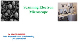
- 1. Scanning Electron Microscope by : MAHESH BIRADAR Dept. of genetics and plant breeding UAS DHARWAD
- 2. History • The first scanning electron microscope with higher magnification were developed by - Manfred vonArdenne 1937. • First SEM developed for bulk samples - Zworykin et al. in 1942 • First commercial SEM developed - Cambridge Scientific Instrument Company as “Stereoscan” in 1965. Manfred vonArdenne
- 3. Scanning Electron Microscope (SEM) • Produces images of a sample by scanning it with a focused beam of electrons in a raster scan pattern. • Electrons interact with atoms and produces various signals that contain information about the sample's surface topography and composition. • Resolution • Depends on the size of the electron spot, which in turn depends on the magnetic electron-optical system which produces the scanning beam. • Is not high enough to image individual atoms, as is possible in the TEM … so that, it is 1-20 nm
- 4. M. von Ardenne's first SEM Schematic representation of SEM
- 5. PRINCIPLE Basic principle : A beam of eˉ is generated by a suitable source ( tungsten filament or a field emission gun). Electron beam is then accelerated through a high voltage (e.g. 20 kV). Passed through a system of apertures and electromagnetic lenses to produce a thin beam of eˉ.
- 6. Then the beam scans the surface of the specimen. Electrons are emitted from the specimen by the action of scanning beam. Collected by a suitable positioned detector.
- 7. +ve -ve
- 9. Electron Gun W hairpin LaB6 crystal FEG
- 10. 2.LENSES Condenser lens –determines the number ofelectrons in the beam which hit the sample by reducing the diameter of the electron beam. Objective lenses -changes the position of thepoint at which the electron are focused on thesample.
- 11. 3. SCANNING COILS Are used to raster/scan the e-beam across the sample surface Thee-beam can be scanned in a rectangular raster across the surface of the sample bymeans of a series of “scan coils” situated above the objective lens. 4. SAMPLE CHAMBER Aplace where the sample was mountedon.
- 12. X-ray photon
- 14. 5. DETECTORS detect the secondary and backscattered electrons. Have + charges
- 17. 6. VACUUM CHAMBER Used to protect the electronic beam from interference with air. control the number of electrons which reach the sample. control the final convergence angle of the electron beam onto the sample 7.Aperture
- 18. HOW THE IMAGE WILLCREATED?
- 19. Beam spot image at different stage of heating
- 20. Topographical Contrast Topographic contrast arises because SE generation depend on the angle of incidence between the beam and sample. Bright Dark
- 21. SAMPLE PREPARATION • Appropriate sized samples will be prepared to fit in to SEM • Mounted rigidly on a specimen holder - specimen stub • For imaging in the SEM, specimens must be 1. Electrically conductive 2. Electrically grounded 1. Cleaning the surface of the specimen 2. Stabilizing the specimen 3. Rinsing the specimen 4. Dehydrating the specimen 5. Drying the specimen 6. Mounting the specimen 7. Coating the specimen
- 22. 1.Cleaning the surface of the specimen • Surface contains many unwanted deposits, such as dust, mud, soil etc 2. Stabilizing the specimen Hard, dry materials such as wood, bone, feathers, dried insects, or shells can be examined with little further treatment, but living cells and tissues and whole, soft- bodied organisms usually require chemical fixation to preserve and stabilize their structure. Stabilization is typically done with fixatives. 3. Rinsing the specimen Sample must be rinsed -- remove excessive fixatives. Fixation -- performed by incubation in a solution of a buffered chemical fixative, such as glutaraldehyde, sometimes in combination with formaldehyde and other fixatives. Fixatives that can be used are:- Aldehydes, Osmium tetroxide, Tanic acid, Thiocarbohydrazides
- 23. 4. Dehydrating the specimen Water must be removed Air-drying causes collapse and shrinkage, this is commonly achieved by replacement of water in the cells with organic solvents such as ethanol or acetone. Dehydration -- performed with a graded series of ethanol or acetone. 5. Drying the specime Specimen should be completely dry Otherwise the sample will be destroyed 6. Mounting the specimen Specimen has to be mounted on the holder Mounted rigidly on a specimen holder called aspecimen stub Dry specimen -- mounted on a specimen stub using an adhesive such as epoxy resin or electrically conductive double-sided adhesive tape.
- 24. Charge-up
- 26. Sample coating is intended to prevent charge-up phenomenon by allowing the charge on the specimen surface go to ground through the coated conductive film. This charge up phenomenon can be prevented by the coating the non-conductor sample with metal (conductor).
- 27. • Coating the specimen • Toincreasetheconductivityofspecimenandtopreventthehighvoltage charge on the specimen Coated with thin layer i.e., 20nm-30nm of conductive metal. All metals are conductive and require no preparation before being used. Coating the specimen Non-metals need to be made conductive, which is done by usinga device called a "sputter coater.” Conductive materials Gold, Gold-palladium Alloy, Platinum, Osmium, Iridium, Tungsten, Chromium and Graphite
- 28. A spider coated with gold
- 29. ADVANTAGES Wide array of applications. 3D & topographical imaging. Versatile information gathered from different detectors. Works faster ( completing SEI, BSE & EDS). Most SEM samples require minimal preparation action. DISADVANTAGES Expensive, large & must be housed in an area free of electric, magnetic and vibration interference. • Maintenance involves keeping a steady voltage, currents to electromagnetic coils and circulation of cool water. • Special training is required to operate an SEM as well as prepare samples. • SEMs are limited to solid, inorganic samples small enough to fit inside the vacuum chamber that can handle moderate vacuum pressure.
- 31. SE Images - Topographic Contrast 1m Defect in a semiconductor device The debris shown here is an oxide fiber got stuck at a semiconductor device detected by SEM Molybdenum trioxide crystals
- 32. SCANNING ELECTRON MICROSCOPIC IMAGE OF THE TONGUE
- 33. Scanning electron micrographs of the early human embryo
- 34. Pollen and Stamens Wool fibers
- 36. THANK YOU…