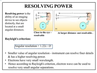
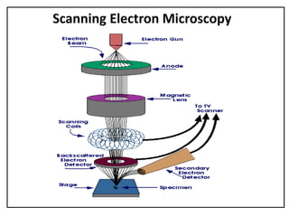
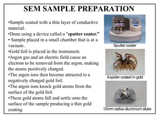
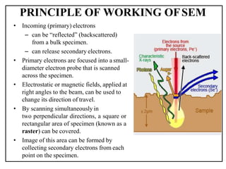
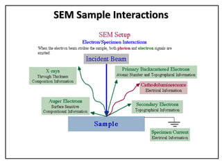
Presented by:
Muhammad Ali Mohsin 2023-MS-MME-1
Presented To:
Prof. Muhammad Asif Rafiq Sb.
INTRODUCTION OF SEM
• Electron Microscopes are scientific instruments that use a beam of
highly energetic electrons to examine objects on a very fine scale.
• This examination can yield information about the topography ,
morphology, composition and crystallographic information.
Mainly 2 types:
• Transmission Electron Microscope (TEM) - allows one the
study of the inner structures.
• Scanning Electron Microscope (SEM) - used to visualize the
surface of objects.
A scanning electron microscope (SEM) is a type of electron
microscope that produces images of a sample by scanning the surface
with a focused beam of electrons.
The electrons interact with atoms in the sample, producing various
signals that contain information about the surface topography and
composition of the sample.
The electron beam is scanned in a raster scan pattern, and the position
of the beam is combined with the intensity of the detected signal to
produce an image.
In the most common SEM mode, secondary electrons emitted by atoms
excited by the electron beam are detected using a secondary electron
detector. The number of secondary electrons that can be detected, and
thus the signal intensity, depends, among other things, on specimen
topography.
 SEM can achieve resolution better than 1 nanometer.
RESOLVING POWER
Close to the eye –
resolvable
At larger distance -not resolvable .
Rayleigh's criterion:
Angular resolution = 1.22λ / D
• Smaller value of angular resolution - instrument can resolve finer details
& has a higher resolving power.
• Electrons have very small wavelength.
• Hence according to Rayleigh's criterion, electron wave can be used to
resolve very small angular separations.
:
Resolving power is the
ability of an imaging
device to see objects
distinctly, that are
located at a small
angular distances.
Topography
Texture/surface of a sample
Morphology
Size, shape, order of particles
Composition
Elemental composition of sample
Crystalline Structure
Arrangement present within sample
What can you see with an SEM?
SEM Micrographs
Crystalline Latex Particles Polymer Hydrogel Surface
Scanning Electron Microscopy (SEM)
Instrumentation:
Essential components of all SEMs include the following:
•Electron Source ("Gun")
•Electron Lenses
•Sample Stage
•Detectors for all signals of interest
•Display / Data output devices
•Infrastructure Requirements:
•Power Supply
•Vacuum System
•Cooling system
•Vibration-free floor
•Room free of ambient magnetic and electric fields
SEMs always have at least one detector (usually a secondary electron
detector), and most have additional detectors.
SEM SAMPLE PREPARATION
Aspider coated in gold
13mm radius aluminium stubs
•Sample coated with a thin layer of conductive
material.
•Done using a device called a "sputter coater.”
• Sample placed in a small chamber that is at a
vacuum .
•Gold foil is placed in the instrument.
•Argon gas and an electric field cause an
electron to be removed from the argon, making
the atoms positively charged.
•The argon ions then become attracted to a
negatively charged gold foil.
•The argon ions knock gold atoms from the
surface of the gold foil.
•These gold atoms fall and settle onto the
surface of the sample producing a thin gold
coating.
Sputtercoater
SEM WORKING
• The electron gun produces an electron beam when tungsten wire is
heated by current.
• This beam is accelerated by the anode.
• The beam travels through electromagnetic fields and lenses, which
focus the beam down toward the sample.
• A mechanism of deflection coils enables to guide the beam so that
it scans the surface of the sample in a rectangular frame.
• When the beam touches the surface of the sample, it produces:
– Secondary electrons (SE)
– Back scattered electrons (BSE)
– X - Rays...
• The emitted SE is collected by SED and convert it into signal that is
sent to a screen which produces final image.
• Additional detectors collect these X-rays, BSE and produce
corresponding images.
• A secondary electron detector attracts the scattered electrons
and, depending on the number of electrons that reach the
detector, registers different levels of brightness on a monitor.
• By reducing the size of the area scanned by the scan coils, the SEM
changes the magnification of the image.
PRINCIPLE OF WORKING OFSEM
• Incoming (primary) electrons
– can be “reflected” (backscattered)
from a bulk specimen.
– can release secondary electrons.
• Primary electrons are focused into a small-
diameter electron probe that is scanned
across the specimen.
• Electrostatic or magnetic fields, applied at
right angles to the beam, can be used to
change its direction of travel.
• By scanning simultaneously in
two perpendicular directions, a square or
rectangular area of specimen (known as a
raster) can be covered.
• Image of this area can be formed by
collecting secondary electrons from each
point on the specimen.
SEM Sample Interactions
• Electron gun consisting of
cathode and anode.
• The condenser lens
controls the amount of
electrons travelling down
the column
• The objective lens focuses
the beam into a spot on the
sample.
• Deflection coil helps to
deflect the electron beam.
• SED attracts the secondary
electrons.
• Additional sensors detect
backscattered electrons
and X-rays.
Advantages
• It gives detailed 3D and topographical imaging and the versatile
information garnered from different detectors.
• This instrument works very fast.
• Modern SEMs allow for the generation of data in digital form.
• Most SEM samples require minimal preparation actions.
Disadvantages
• SEMs are expensive and large.
• Special training is required to operate an SEM.
• The preparation of samples can result in artifacts.
• SEMs are limited to solid samples.
• SEMs carry a small risk of radiation exposure associated with the
electrons that scatter from beneath the sample surface.
ADVANTAGES & DISADVANTAGES OF SEM
RECENT DEVELOPMENTS
• Three famous physicists, Harald H. Rose , Knut W. Urban and
Maximillian Haider have received the Wolf-prize in physics 2011
for the realization of aberration-corrected electron microscopy.
• Aberrations are intrinsic imperfections of electron lenses.
• Those aberrations are reduced by installing in a microscope a set of
specially designed auxiliary "lenses" which are called aberration
correctors.
• They designed a novel aberration corrector thereby improving
resolution of transmission electron microscope.
CONCLUSION
• Since its invention, electron microscope has been a valuable tool in
the development of scientific theory
• It has contributed greatly to biology, medicine and material
sciences.
• This wide spread use because they permit the observation of
materials on a nanometer (nm) to micrometer (μm) scale.
• Although SEMs and TEMs are large, expensive pieces of
equipments, they remain popular among researchers due to the high-
resolution and detailed images they produce.

scanning electron microscope for analysis

  • 2.
    Presented by: Muhammad AliMohsin 2023-MS-MME-1 Presented To: Prof. Muhammad Asif Rafiq Sb.
  • 3.
    INTRODUCTION OF SEM •Electron Microscopes are scientific instruments that use a beam of highly energetic electrons to examine objects on a very fine scale. • This examination can yield information about the topography , morphology, composition and crystallographic information. Mainly 2 types: • Transmission Electron Microscope (TEM) - allows one the study of the inner structures. • Scanning Electron Microscope (SEM) - used to visualize the surface of objects.
  • 4.
    A scanning electronmicroscope (SEM) is a type of electron microscope that produces images of a sample by scanning the surface with a focused beam of electrons. The electrons interact with atoms in the sample, producing various signals that contain information about the surface topography and composition of the sample. The electron beam is scanned in a raster scan pattern, and the position of the beam is combined with the intensity of the detected signal to produce an image. In the most common SEM mode, secondary electrons emitted by atoms excited by the electron beam are detected using a secondary electron detector. The number of secondary electrons that can be detected, and thus the signal intensity, depends, among other things, on specimen topography.  SEM can achieve resolution better than 1 nanometer.
  • 5.
    RESOLVING POWER Close tothe eye – resolvable At larger distance -not resolvable . Rayleigh's criterion: Angular resolution = 1.22λ / D • Smaller value of angular resolution - instrument can resolve finer details & has a higher resolving power. • Electrons have very small wavelength. • Hence according to Rayleigh's criterion, electron wave can be used to resolve very small angular separations. : Resolving power is the ability of an imaging device to see objects distinctly, that are located at a small angular distances.
  • 6.
    Topography Texture/surface of asample Morphology Size, shape, order of particles Composition Elemental composition of sample Crystalline Structure Arrangement present within sample What can you see with an SEM?
  • 7.
    SEM Micrographs Crystalline LatexParticles Polymer Hydrogel Surface
  • 8.
    Scanning Electron Microscopy(SEM) Instrumentation: Essential components of all SEMs include the following: •Electron Source ("Gun") •Electron Lenses •Sample Stage •Detectors for all signals of interest •Display / Data output devices •Infrastructure Requirements: •Power Supply •Vacuum System •Cooling system •Vibration-free floor •Room free of ambient magnetic and electric fields SEMs always have at least one detector (usually a secondary electron detector), and most have additional detectors.
  • 10.
    SEM SAMPLE PREPARATION Aspidercoated in gold 13mm radius aluminium stubs •Sample coated with a thin layer of conductive material. •Done using a device called a "sputter coater.” • Sample placed in a small chamber that is at a vacuum . •Gold foil is placed in the instrument. •Argon gas and an electric field cause an electron to be removed from the argon, making the atoms positively charged. •The argon ions then become attracted to a negatively charged gold foil. •The argon ions knock gold atoms from the surface of the gold foil. •These gold atoms fall and settle onto the surface of the sample producing a thin gold coating. Sputtercoater
  • 11.
    SEM WORKING • Theelectron gun produces an electron beam when tungsten wire is heated by current. • This beam is accelerated by the anode. • The beam travels through electromagnetic fields and lenses, which focus the beam down toward the sample. • A mechanism of deflection coils enables to guide the beam so that it scans the surface of the sample in a rectangular frame. • When the beam touches the surface of the sample, it produces: – Secondary electrons (SE) – Back scattered electrons (BSE) – X - Rays... • The emitted SE is collected by SED and convert it into signal that is sent to a screen which produces final image. • Additional detectors collect these X-rays, BSE and produce corresponding images.
  • 12.
    • A secondaryelectron detector attracts the scattered electrons and, depending on the number of electrons that reach the detector, registers different levels of brightness on a monitor. • By reducing the size of the area scanned by the scan coils, the SEM changes the magnification of the image.
  • 13.
    PRINCIPLE OF WORKINGOFSEM • Incoming (primary) electrons – can be “reflected” (backscattered) from a bulk specimen. – can release secondary electrons. • Primary electrons are focused into a small- diameter electron probe that is scanned across the specimen. • Electrostatic or magnetic fields, applied at right angles to the beam, can be used to change its direction of travel. • By scanning simultaneously in two perpendicular directions, a square or rectangular area of specimen (known as a raster) can be covered. • Image of this area can be formed by collecting secondary electrons from each point on the specimen.
  • 14.
  • 15.
    • Electron gunconsisting of cathode and anode. • The condenser lens controls the amount of electrons travelling down the column • The objective lens focuses the beam into a spot on the sample. • Deflection coil helps to deflect the electron beam. • SED attracts the secondary electrons. • Additional sensors detect backscattered electrons and X-rays.
  • 17.
    Advantages • It givesdetailed 3D and topographical imaging and the versatile information garnered from different detectors. • This instrument works very fast. • Modern SEMs allow for the generation of data in digital form. • Most SEM samples require minimal preparation actions. Disadvantages • SEMs are expensive and large. • Special training is required to operate an SEM. • The preparation of samples can result in artifacts. • SEMs are limited to solid samples. • SEMs carry a small risk of radiation exposure associated with the electrons that scatter from beneath the sample surface. ADVANTAGES & DISADVANTAGES OF SEM
  • 18.
    RECENT DEVELOPMENTS • Threefamous physicists, Harald H. Rose , Knut W. Urban and Maximillian Haider have received the Wolf-prize in physics 2011 for the realization of aberration-corrected electron microscopy. • Aberrations are intrinsic imperfections of electron lenses. • Those aberrations are reduced by installing in a microscope a set of specially designed auxiliary "lenses" which are called aberration correctors. • They designed a novel aberration corrector thereby improving resolution of transmission electron microscope.
  • 19.
    CONCLUSION • Since itsinvention, electron microscope has been a valuable tool in the development of scientific theory • It has contributed greatly to biology, medicine and material sciences. • This wide spread use because they permit the observation of materials on a nanometer (nm) to micrometer (μm) scale. • Although SEMs and TEMs are large, expensive pieces of equipments, they remain popular among researchers due to the high- resolution and detailed images they produce.