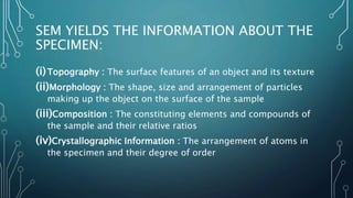
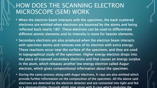
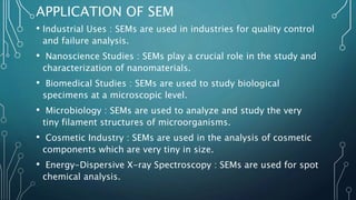
SEMINAR ON SCANNING
ELECTRON MICROSCOPE
(SEM)
KONGU ENGINEERING COLLEGE
BY:
NAVANEETHAN K V [23MER024]
SRISABARI S [23MER048]
DATE: 05.01.2024
INTRODUCTION
• The first Scanning Electron Microscope was initially made by
Mafred von Ardenne in 1937 with an aim to surpass the
transmission electron Microscope.
• He also aimed at reducing the problems of chromatic
aberrations images produced by the Transmission electron
Microscopes.
• SEM provides high-resolution , three-dimensional image.
Introduction
SCANNING ELECTRON MICROSCOPE
(SEM) :
The Scanning Electron Microscope (SEM) uses a low-energy
electron beam to scan microorganisms. It was developed due to
the limited resolution of light microscopes, as electron
microscopes have shorter wavelengths, enabling better
resolution.
PRINCIPLE OF SCANNING ELECTRON
MICROSCOPE (SEM):
• The Scanning Electron Microscope (SEM) uses kinetic energy to
generate signals from secondary and backscattered electrons.
These electrons, emitted from the specimen, help create
images. Secondary electrons reveal the specimen's morphology
and topography, while backscattered electrons highlight
elemental composition contrasts.
PARTS OF A SCANNING ELECTRON
MICROSCOPE (SEM):
• Electron Source
• Lenses
• Scanning Coil
• Detector
• CRT(Cathode Ray Tube) - A special vacuum tube that creates an image
• Power supply
• Vacuum system
SEM YIELDS THE INFORMATION ABOUT THE
SPECIMEN:
(i)Topography : The surface features of an object and its texture
(ii)Morphology : The shape, size and arrangement of particles
making up the object on the surface of the sample
(iii)Composition : The constituting elements and compounds of
the sample and their relative ratios
(iv)Crystallographic Information : The arrangement of atoms in
the specimen and their degree of order
HOW DOES THE SCANNING ELECTRON
MICROSCOPE (SEM) WORK
• When the electron beam interacts with the specimen, the back scattered
electrons are emitted when electrons are bounced by the atoms and being
reflected back nearly 180°. These electrons can be used to differentiate
different atomic elements and its intensity is more for heavier elements.
• Secondary electrons are also produced when the electron beam interacts
with specimen atoms and removes one of its electron with extra energy.
These reactions occur near the surface of the specimen, and they are used
in topographical study of the specimen. Higher energy electron drops into
the place of exposed secondary electrons and that causes an energy surplus
in the atom, which releases another low energy electron called Augur
electron, which gives compositional information about the specimen.
• During the same process along with Augur electrons, X-rays are also emitted which
provide further information on the composition of the specimen. All the above said
electrons are detected by the electron detector and are converted into light and fed
DIAGRAM OF SCANNING ELECTRON
MICROSCOPE(SEM)
APPLICATION OF SEM
• Industrial Uses : SEMs are used in industries for quality control
and failure analysis.
• Nanoscience Studies : SEMs play a crucial role in the study and
characterization of nanomaterials.
• Biomedical Studies : SEMs are used to study biological
specimens at a microscopic level.
• Microbiology : SEMs are used to analyze and study the very
tiny filament structures of microorganisms.
• Cosmetic Industry : SEMs are used in the analysis of cosmetic
components which are very tiny in size.
• Energy-Dispersive X-ray Spectroscopy : SEMs are used for spot
chemical analysis.
MERITS AND DEMERITS:
• Merits:
1. Three-dimensional image of the object is obtained.
2. Object image has large depth of focus.
3. It can be used to examine specimen of large thickness.
4. Image can be viewed directly on the screen.
5. 3,00,000 times greater than that of the size of the object
magnification can be obtained.
• Demerits:
The resolution of the image is limited to 10-20 nm, hence it is very
poor.
THANK
YOU

Scanning Electron Microscope (SEM).pptx

  • 1.
    SEMINAR ON SCANNING ELECTRONMICROSCOPE (SEM) KONGU ENGINEERING COLLEGE BY: NAVANEETHAN K V [23MER024] SRISABARI S [23MER048] DATE: 05.01.2024
  • 2.
    INTRODUCTION • The firstScanning Electron Microscope was initially made by Mafred von Ardenne in 1937 with an aim to surpass the transmission electron Microscope. • He also aimed at reducing the problems of chromatic aberrations images produced by the Transmission electron Microscopes. • SEM provides high-resolution , three-dimensional image. Introduction
  • 3.
    SCANNING ELECTRON MICROSCOPE (SEM): The Scanning Electron Microscope (SEM) uses a low-energy electron beam to scan microorganisms. It was developed due to the limited resolution of light microscopes, as electron microscopes have shorter wavelengths, enabling better resolution.
  • 4.
    PRINCIPLE OF SCANNINGELECTRON MICROSCOPE (SEM): • The Scanning Electron Microscope (SEM) uses kinetic energy to generate signals from secondary and backscattered electrons. These electrons, emitted from the specimen, help create images. Secondary electrons reveal the specimen's morphology and topography, while backscattered electrons highlight elemental composition contrasts.
  • 5.
    PARTS OF ASCANNING ELECTRON MICROSCOPE (SEM): • Electron Source • Lenses • Scanning Coil • Detector • CRT(Cathode Ray Tube) - A special vacuum tube that creates an image • Power supply • Vacuum system
  • 6.
    SEM YIELDS THEINFORMATION ABOUT THE SPECIMEN: (i)Topography : The surface features of an object and its texture (ii)Morphology : The shape, size and arrangement of particles making up the object on the surface of the sample (iii)Composition : The constituting elements and compounds of the sample and their relative ratios (iv)Crystallographic Information : The arrangement of atoms in the specimen and their degree of order
  • 7.
    HOW DOES THESCANNING ELECTRON MICROSCOPE (SEM) WORK • When the electron beam interacts with the specimen, the back scattered electrons are emitted when electrons are bounced by the atoms and being reflected back nearly 180°. These electrons can be used to differentiate different atomic elements and its intensity is more for heavier elements. • Secondary electrons are also produced when the electron beam interacts with specimen atoms and removes one of its electron with extra energy. These reactions occur near the surface of the specimen, and they are used in topographical study of the specimen. Higher energy electron drops into the place of exposed secondary electrons and that causes an energy surplus in the atom, which releases another low energy electron called Augur electron, which gives compositional information about the specimen. • During the same process along with Augur electrons, X-rays are also emitted which provide further information on the composition of the specimen. All the above said electrons are detected by the electron detector and are converted into light and fed
  • 8.
    DIAGRAM OF SCANNINGELECTRON MICROSCOPE(SEM)
  • 9.
    APPLICATION OF SEM •Industrial Uses : SEMs are used in industries for quality control and failure analysis. • Nanoscience Studies : SEMs play a crucial role in the study and characterization of nanomaterials. • Biomedical Studies : SEMs are used to study biological specimens at a microscopic level. • Microbiology : SEMs are used to analyze and study the very tiny filament structures of microorganisms. • Cosmetic Industry : SEMs are used in the analysis of cosmetic components which are very tiny in size. • Energy-Dispersive X-ray Spectroscopy : SEMs are used for spot chemical analysis.
  • 10.
    MERITS AND DEMERITS: •Merits: 1. Three-dimensional image of the object is obtained. 2. Object image has large depth of focus. 3. It can be used to examine specimen of large thickness. 4. Image can be viewed directly on the screen. 5. 3,00,000 times greater than that of the size of the object magnification can be obtained. • Demerits: The resolution of the image is limited to 10-20 nm, hence it is very poor.
  • 11.