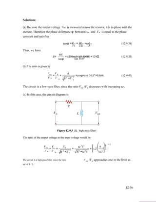
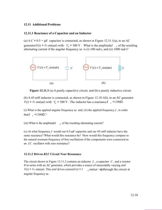
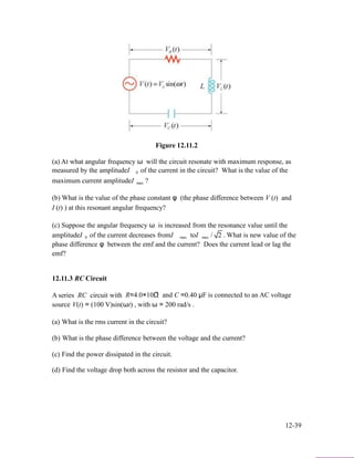
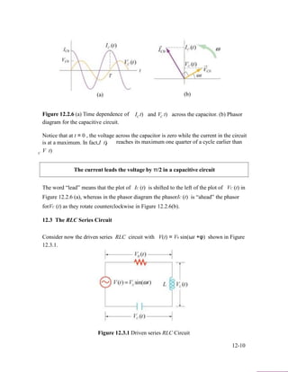
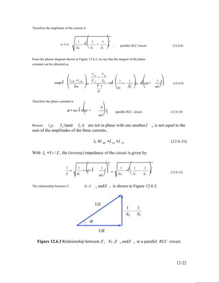
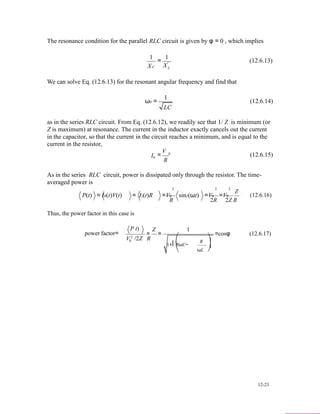
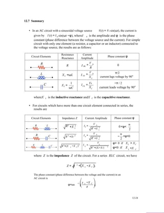
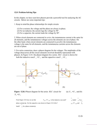
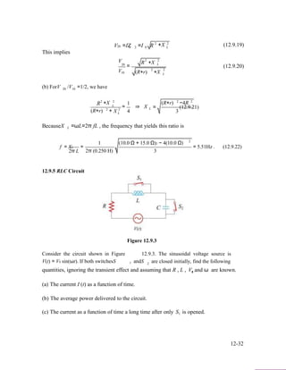
This document section describes alternating current (AC) circuits containing a single circuit element: resistor, inductor, or capacitor, connected to an AC voltage source. For a resistive circuit, the current and voltage are in phase. For an inductive circuit, the current lags the voltage by 90 degrees. For a capacitive circuit, the current leads the voltage by 90 degrees. The document defines important concepts such as reactance, impedance, and phasor diagrams for analyzing AC circuits.


![(d) The capacitance C if bothS andS are opened for a long time, with the current and1 2
voltage in phase.
(e) The impedance of the circuit when both S and S are opened.1 2
(f) The maximum energy stored in the capacitor during oscillations.
(g) The maximum energy stored in the inductor during oscillations.
(h) The phase difference between the current and the voltage if the frequency of V (t) is
doubled.
(i) The frequency at which the inductive reactanceX
reactanceX
L is equal to half the capacitive
C
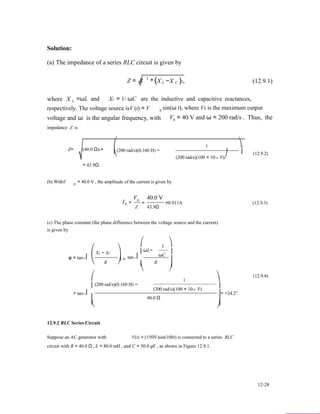
Solutions:
(a) When both switchesS andS are closed, the current only goes through the generator1 2
and the resistor, so the total impedance of the circuit is R and the current is
IR (t) =V0 sin(ωt) . (12.9.23)
R
(b) The average power is given by
P(t) = IR(t)V(t)
2 2
=V0 sin2 (ωt) =V0 (12.9.24)
R 2R
(c) If only S is opened, after a long time the current will pass through the generator, the1
resistor and the inductor. For this RL circuit, the impedance becomes
Z=
R
and the phase constant φ is
2
1
+X
=
2
L R2
1
+ω2
, (12.9.25)
2
L
φ=tan −1 ⎛ωL⎞
⎜ ⎟ (12.9.26)
Thus, the current as a function of time is
I(t) = I0 sin(ωt −φ) =
⎝R
V0
⎠
sin[ωt − tan−1(ω L / R)]. (12.9.27)
R2 +ω2 L2
12-33](https://image.slidesharecdn.com/rlccircuit-170508180421/85/R-L-C-circuit-34-320.jpg)