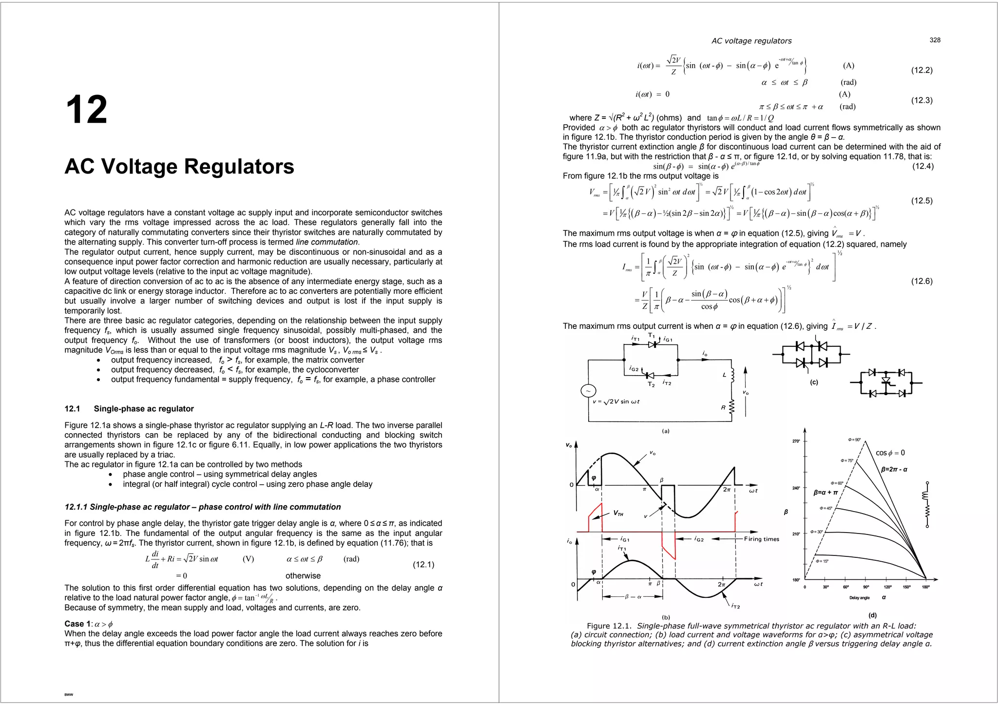
AC voltage regulators vary the RMS voltage across an AC load by using semiconductor switches to control the phase angle of the AC supply voltage impressed on the load. There are three categories depending on the relationship between the input and output frequencies: output frequency can be increased, decreased, or equal to the supply frequency. Regulation is achieved by phase angle control where the thyristor firing delay angle is varied between 0 and π radians. The output voltage, current, and power vary as functions of the firing delay angle. Harmonic reduction may be required since the output current is discontinuous and non-sinusoidal at low output voltages.
![351 Power Electronics
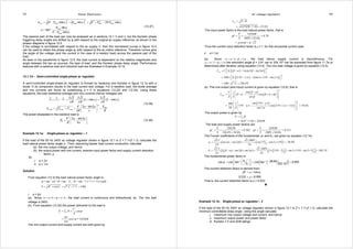
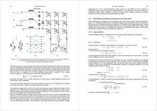
12.3 Single-phase ac chopper regulator – commutable switches
An ac step-down chopper is shown in figure 12.9a. The switches T1 and T3 (shown as reverse blocking
IGBTs) impress the ac supply across the load while T2 and T4 provide load current freewheel paths
when the main switches T1 and T3 are turned off. In order to prevent the supply being shorted, switches
T1 and T4 can not be on simultaneously when the ac supply is in a positive half cycle, while T2 and T3
can not both be on during a negative half cycle of the ac supply. Zero voltage information is necessary.
If the rms supply voltage is V and the on-state duty cycle of T1 and T3 is δ, then rms output voltage Vo is
o V = δV (12.63)
When the sinusoidal supply is modulated by a high frequency rectangular-wave carrier ωs (2πfs), which
is the switching frequency, the ac output is at the same frequency as the supply fo but the fundamental
magnitude is proportional to the rectangular wave duty cycle δ, as shown in figure 12.9b. Being based
on a modulation technique, the output harmonics involve the fundamental at the supply frequency fo and
components related to the high frequency rectangular carrier waveform fs. The output voltage is given by
{ ( ) ( ) } .
.
Σ (12.64)
δ ω δ ω ω ω ω
1
2
2 sin sin sin sin o o o c o c
n
V
V V t n n t n t
n
∀
= + + − −
The carrier (switching frequency) components can be filtered by using an output L-C filter, as shown in
figure 12.9a, which has a cut-off frequency of f½ complying with fo f½ fs.
12.4 Three-phase ac regulator
12.4.1 Fully-controlled three-phase ac regulator with wye load and isolated neutral
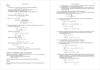
The power to a three-phase star or delta-connected load may be controlled by the ac regulator shown in
figure 12.10a with a star-connected load shown. The circuit is commonly used to soft start three-phase
induction motors. If a neutral connection is made, load current can flow provided at least one thyristor is
conducting. At high power levels, neutral connection is to be avoided, because of load triplen currents
that may flow through the phase inputs and the neutral. With a balanced delta connected load, no triplen
or even harmonic currents occur.
If the regulator devices in figure 12.10a, without the neutral connected, were diodes, each would
conduct for ½π in the order T1 to T6 at ⅓π radians apart. As thyristors, conduction is from α to ½π.
Purely resistive load
In the fully controlled ac regulator of figure 12.10a without a neutral connection, at least two devices
must conduct for power to be delivered to the load. The thyristor trigger sequence is as follows. If
thyristor T1 is triggered at α, then for a symmetrical three-phase load voltage, the other trigger angles are
T3 at α + ⅔π and T5 at α + 4π/3. For the antiparallel devices, T4 (which is in antiparallel with T1) is
triggered at α + π, T6 at α + 5π/3, and finally T2 at α + 7π/3.
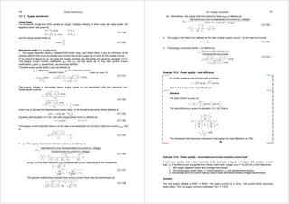
Figure 12.10b shows resistive load, line-to-neutral voltage waveforms (which are symmetrical about zero
volts) for four different phase delay angles, α. Three distinctive conduction periods, plus a non-conduction
period, exist. The waveforms in figure 12.10b are useful in determining the required bounds
of integration. When three regulator thyristors conduct, the voltage (and the current) is of the
formV 3 sinφ ∧ , while when two devices conduct, the voltage (and the current) is of the form
∧
V 2 sin ( φ − 1 6π
)
.
V ∧
is the maximum line voltage,√3 √2V.
i. 0 ≤ α ≤ ⅓π [mode 3/2] – alternating every π between 2 and 3 conducting thyristors,
Full output occurs when α = 0, when the load voltage is the supply voltage and each thyristor
conducts for π. For α ≤ ⅓π, in each half cycle, three alternating devices conduct and one will be
turned off by natural commutation. The output voltage is continuous. Only for ωt ≤ ⅓π can three
sequential devices be on simultaneously.
Examination of the α = ¼π waveform in figure 12.10b shows the voltage waveform is made from
five sinusoidal segments. The rms load voltage per phase (line to neutral), for a resistive load, is
π 1 π α 2
π
+ +
∫ ∫ ( )
∫
+
3 3 3
d d d
φ φ φ φ φ
1 2 1 2 φ +
π
1 2
3 4 3
∧ +
α π π α
=
∫ ∫ rms
π π +
α π
φ φ φ
+ ( )
+
1
6
1 1
3 3
2
3
1 2 φ −
1
π
1 2
4 6
3
2 2
3 3
½
1 sin sin sin
sin sin
+
π πα
V V
d d
3 3 ½
2 41 sin 2 π π = = − α + α rms rms V I R V (12.65)
AC voltage regulators 352
Optional tapped neutral
½(va-vb)
ia
ib
v 2 V sin
t
v 2 V sin
t
v 2 V sin
t
=
.
= −
.
= −
.
a
b
c
½(va-vc)
½(va-vc)
va
½(va-vc) va
T1
T2
T6
T1
T5
T6
T6
T1
T1
T2
T2
T3
T5
T6
T1
T6
T1
T2
T1
T2
T6
T1
T5
T6
T6
T1
T1
T2
(c)
ZL
ZL
ZL
ic
a
b
c
L
O
A
D
( ω
)
( ω 2
π
)
3
( ω 4
π
)
3
Figure 12.10. Three-phase ac full-wave voltage controller: (a) circuit connection with a star load;
(b) phase a, line-to-load neutral voltage waveforms for four firing delay angles; and (c) delta load.
The Fourier coefficients of the fundamental frequency are
( ) ( ) 1 1
4
3
3 3
cos 2 1 sin2 2
a V α b V α π α
= − = + − (12.66)
4 4
π π
Using the five integration terms as in equation (12.65), not squared, gives the average half-wave
(half-cycle) load voltage, hence specifies the average thyristor current requirement with a resistive
load. That is
∫
V I R V t d t
( )
½cycle
o T
½cycle
1
2 2 sin
2
2
2 1 cos
o T
V
V I R
π
α
ω ω
π
α
π
= × =
= × = +
(12.67)
The thyristor maximum average current is when α = 0, that is
2
T
V
I
πR
∧
= .
ii. ⅓π ≤ α ≤ ½π [mode 2/2] – two conducting thyristors
The turning on of one device naturally commutates another conducting device and only two phases
can be conducting, that is, only two thyristors conduct at any time. Two phases experience half the](https://image.slidesharecdn.com/chapter12-1-140915051510-phpapp01/85/Chapter-12-1-microelectronics-13-320.jpg)
![353 Power Electronics
difference of their input phase voltages, while the off thyristor is reverse biased by 3/2 its phase
voltage, (off with zero current). The line-to-neutral load voltage waveforms for α = ⅓π and ½π,
which are continuous, are shown in figures 12.10b.
Examination of the α = ⅓π or α = ½π waveforms in figure 12.10b show the voltage waveform is
comprised from two segments. The rms load voltage per phase, for a resistive load, is
{ ( ) ( ) } 1 2
∧ V V ∫ π + α d ∫ π +
α
= + d
rms 3 π 1 2 φ + 1 π φ 3
1 2
φ −
1
π φ
4 6 4
6
1
3
½
1 sin sin
+
α πα
( ) ½ ½
V = I R = V 3 3
3 3
rms rms ½ + 9 sin 2 α + 8 π 8 π cos 2 α = V ½ + 4 π sin 2 α + π
6
(12.68)
The Fourier co-efficients of the fundamental frequency are
3 3
( ( )) ( 2
+ ( )) 1 1
a V cos 2 α cos 2 α π b V π sin2 α sin2
α π
= − − = − − (12.69)
3 3 3
4 4
π π
The non-fundamental harmonic magnitudes are independent of α, and are given by
3
( ) ( )6
sin 1 for 6 1 1,2,3,..
V = × V × h ± h = k ± k
=
h 1 h
π
π
±
(12.70)
Using the same two integration terms, not squared, gives the average half-wave (half-cycle) load
voltage, hence specifies the average thyristor current with a resistive load. That is
( ) ( ) ½cycle
∫ ∫
V I R V t d t t d t
½cycle
1 2
3 1 3 1
= × = + + −
6 1 6
3
1
2 3 2 sin sin
2
3 2
2 sin
3
o T
o T
V
V I R
π α π α
α πα
ω π ω ω π ω
π
π
α
π
+ +
+
= × = +
(12.71)
iii. ½π ≤ α ≤ π [mode 2/0] – either 2 or no conducting thyristors
Two devices must be triggered in order to establish load current and only two devices conduct at
anytime. Line-to-neutral zero voltage periods occur and each device must be retriggered ⅓π after
the initial trigger pulse. These zero output periods (discontinuous load voltage) which develop for α
≥ ½π can be seen in figure 12.10b and are due to a previously on device commutating at ωt = π
then re-conducting at α +⅓π. Except for regulator start up, the second firing pulse is not necessary
if α ≤ ½π.
Examination of the α = ¾π waveform in figure 12.10b shows the voltage waveform is made from
two discontinuous voltage segments. The rms load voltage per phase, for a resistive load, is
{ ( ) ( ) } 5 7
= + rms ∫ ∫ V V d d
π π
1 sin sin
6 φ + π θ 6
π φ −
π φ
1 1
6 1 6
3
½
1 2 1 2
4 4
α πα
∧
+
( ) ½ ½ 5 3 3 3 3 5 3 3 1
4 2π 8π sin 2 8π cos 2 4 2π 4π sin 2 3 = = − α + α + α = − α + α + π rms rms V I R V V (12.72)
The Fourier co-efficients of the fundamental frequency are
3 3
( 1 cos2 ( 1 )) ( 5 2 sin2
( 1
)) 1 3 1
3 3
a V α π b V π α α π
= − + − = − − − (12.73)
4 4
π π
Using the same two integration terms, not squared, gives the average half-wave (half-cycle) load
voltage, hence specifies the average thyristor current with a resistive load. That is
½cycle 3 2
V
( ( )) V I R α π
o 2 T 1 cos 6
= × = + + (12.74)
π
iv. π ≤ α ≤ π [mode 0] – no conducting thyristors
The interphase voltage falls to zero at α = π, hence for α ≥ π the output becomes zero.
In each case the phase current and line to line voltage are related by V = 3 I R and the peak
Lrms rms voltage is V l = 2 V = 6 V . For a resistive load, load power 3 I 2 R for all load types, and V = I R
. L rms rms rms Both the line input and load current harmonics occur at 6n±1 times the fundamental.
Inductive-resistive load
Once inductance is incorporated into the load, current can only flow if the phase angle is at least equal
to the load phase angle, given by φ = tan − 1 ω L
.Due to the possibility of continuation of the load current
R
because of the stored inductive load energy, only two thyristor operational modes occur. The initial
mode at φ ≤ α operates with three then two conducting thyristors mode [3/2], then as the control angle
increases, operation in a mode [2/0] occurs with either two devices conducting or all three off, until α =
AC voltage regulators 354
π. The transitions between 3 and 2 thyristors conducting and between the two modes involves
solutions to transcendental equations, and the rms output voltage, whence currents, depend on the
solution to these equations.
Purely inductive load
For a purely inductive load the natural ac power factor angle is ½π, where the current lags the voltage
by ½π. Therefore control for such a load starts from α = ½π, and since the average inductor voltage
must be zero, conduction is symmetrical about π and ceases at 2π - α. The conduction period is 2(π- α).
Two distinct conduction periods exist.
i. ½π ≤ α ≤ ⅔π [mode 3/2] – either 2 or 3 conducting thyristors
Either two or three phases conduct and five integration terms give the load half cycle average
voltage, whence average thyristor current, as
½cycle 2 2
V
( ) V α α
2cos 3 sin 1 3 o
= − + + (12.75)
π
The thyristor maximum average current is when α=½π.
When only two thyristors conduct, the phase current during the conduction period is given by
= − +
( ) 2 3 3
cos cos
2 2 6
V
i t t
L
π
ω α ω
ω
(12.76)
The load phase rms voltage and current are
( )
½
( ( ) )
½
5 3 3
2 2
5 3 6 9
2 2
= − +
α α
2
sin2
7 cos sin2
V V
rms
rms
V
I
= − + − +
L
π π
α α α α
π π π
ω
(12.77)
The magnitude of the sin term fundamental (a1 = 0) is
( ) 1 1 1
5
3
3
V b V π 2 α sin2
α I ωL
= = − + = (12.78)
2
π
while the remaining harmonics (ah = 0) are given by
3 sin( 1) sin( 1)
h h
V b V
α α
h h 1 1
h h
π
+ −
= = + + −
(12.79)
ii. ⅔π ≤ α ≤ π [mode 2/0] – either 2 or no conducting thyristors
Discontinuous current flows in two phases, in two periods per half cycle and two integration terms
(reduced to one after time shifting) give the load half cycle average voltage, whence average
thyristor current, as
½cycle 2 2
V
( ( )) V α π
o 3 1 cos 6
= + + (12.80)
π
which reduces to zero volts at α = π.
The average thyristor current is given by
5
π α
1 3 3 2
∫
2 cos cos
2 2 6 6
3 2 5
2 cos 2sin
α
2 3 6 6
T
V
I t d t
L
V
L
π π
α ω ω
π ω
π π
π α α α
πω
−
= × + − +
= − + − +
(12.81)
When two thyristors conduct, the phase current during the conduction period is given by
= + − +
( ) 2 3
cos cos
2 6 6
V
i t t
L
π π
ω α ω
ω
(12.82)
The load phase rms voltage and current are
( ( ))
½
5 3 3 1
2 2 3 sin 2
5 3 6 9
= − + − ( + ) + ( + )
½
= − + +
5 cos sin2
2 1 1
6 6
V V
2 2
rms
rms
V
I
L
π π α α π
α α
α π α π
ω π π π
(12.83)](https://image.slidesharecdn.com/chapter12-1-140915051510-phpapp01/85/Chapter-12-1-microelectronics-14-320.jpg)
![355 Power Electronics
The magnitude of the sin term fundamental (a1 = 0) is
α α π
∓
V b V h k
1
0.75
0.5
0.25
0
( 5 ( 1
)) 1 1 3 3
1
V b V π α α π I ωL
= = − − − = (12.84)
h h
Equation
(12.77)
0 30 60 90 120 150
delay angle α
normalised rms voltages, R and L loads
Equation
(12.65)
Equation
(12.68)
Equation
(12.72)
Equation
(12.83)
rms V
V
VR VL
1
0.75
0.5
0.25
0
Equation
(12.75)
0 30 60 90 120 150
delay angle α
normalised ave ½ half cycle voltages, R and L loads
Equation
(12.67)
Equation
(12.71)
Equation
(12.74)
Equation
(12.80)
2√2/π
V½R
V½L
½
o V
V
1
0.75
0.5
0.25
0
0 30 60 90 120 150
delay angle α
normalised output current, with L load
Equation
(12.77)
Equation
(12.83)
IL
I ω
L
L V
1
0.75
0.5
0.25
0
Equation
(12.78)
Equation
(12.73)
0 30 60 90 120 150
delay angle α
normalised fundamental output voltage R L load
Equation
(12.66)
Equation
(12.69)
Equation
(12.84)
1 v
V
VRo
VLo
(a) (b)
(c) (d)
3
2 sin2
2
π
while the remaining harmonics (ah = 0) are given by
( ) ( )( 1 )
3 3 sin 1 sin 1
for 6 1
h h 1 1
h h
π
± −
= = ± + = ±
∓
∓
(12.85)
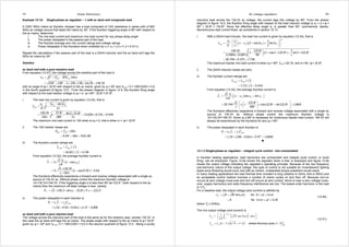
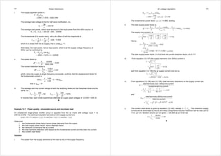
Various normalised voltage and current characteristics for resistive and inductive equations derived are
shown in figure 12.11.
Figure 12.11. Three-phase ac full-wave voltage controller characteristics for purely resistive and
inductive loads: (a) normalised rms output voltages; (b) normalised half-cycle average voltages; (c)
normalised output current for a purely inductive load; and (d) fundamental ac output voltage.
AC voltage regulators 356
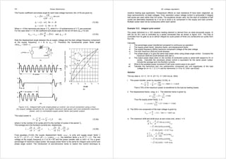
12.4.2 Fully-controlled three-phase ac regulator with wye load and neutral connected
If the load and supply neutral is connected in the three phase thyristor controller with a wye load as
shown dashed in figure 12.10a, then (possibly undesirably) neutral current can flow and each of the
three loads can be controlled independently. Undesirably, the third harmonic and its odd multiples are
algebraically summed and returned to the supply via the neutral connection. At any instant iN = ia + ib + ic.
For a resistive balanced load there are three modes of thyristor conduction.
When 3 thyristors conduct ia + ib + ic =IN = 0, two thyristor conduct ( ) .
I = I = V R ωt .
I
I
1
0.75
0.5
0.25
0
π
α
+ = − −
V
= × −
V
I
= − (12.87)
2 2
π π
α
+ = − − +
3 2 sin 3 2 sin N
I V R t dt V R t dt
∫ ∫
V
I
= × −
V
I
= − (12.89)
V V
= − = (12.90)
0 30 60 90 120 150 180
delay angle
rms and average neutral current
Equation
(12.86)
Equation
(12.87)
Equation
(12.88)
Equation
(12.89)
Equation
(12.91)
Equation
(12.92)
I V t = − R ω − π , and for
rms
neutral
current
average
neutral
current
rms I
V
R
N I
V
R
43
2 sin N
one thyristor . 2 sin
N T
Mode [3/2] 0 ≤ α ≤ ⅓π
Periods of zero neutral current occur when three thyristors conduct and the rms of the discontinuous
neutral current is given by
( ) .
3
3
2
2 4
3
3 2 sin N
I V t dt R
π
ω π
π
∫
( )
½
½
3
sin2 N
R
α α
π
(12.86)
The average neutral current is
( ) 3 2
1 cos N
R
α
π
At α = 0°, no neutral current flows since the load is seen as a balance load supplied by the three-phase
ac supply, without an interposing controller.
Mode [2/1] ⅓π ≤ α ≤ ⅔π
From α to ⅔π two phase conduct and after ⅔π the neutral current is due to one thyristor conducting.
The rms neutral current is given by
( ) . .
2
3 3
2
3
2 4
3
π
α
ω π ω
π π
½
. 2 3 3
1 cos N
R
α
π
(12.88)
Maximum rms neutral current occurs at α = ½π, when IN = V/R.
The average neutral current is
( ) 3 2
3 sin 1 N
R
α
π
The maximum average neutral current, at α = ½π, is
( ) 3 2
N 3 1 0.9886
πR R
Figure 12.12. Three-phase ac full-wave voltage neutral-connected controller with resistive load,
normalised rms neutral current and normalised average neutral current.](https://image.slidesharecdn.com/chapter12-1-140915051510-phpapp01/85/Chapter-12-1-microelectronics-15-320.jpg)
![357 Power Electronics
Mode [1/0] ⅔π ≤ α ≤ π
The neutral current is due to only one thyristor conducting. The rms neutral current is given by
= + (12.92)
= − + = ≤ ≤ rms rms V V IR (12.94)
1.75
1.5
1.25
1
0.75
0.5
0.25
0
Equation
(12.98)
0 30 60 90 120 150 180
delay angle
= × − +
α α
rms line current
Semi-controlled
rms I
V
R
controlled
Equation
(12.95)
Equation
(12.96)
Equation
(12.97)
Equation
(12.99)
= .
2
π
2 3 2 sin
N
I V R t dt
α
ω
π
∫
( )
½
½
3
V
I
sin2 N
R
π α α
π
(12.91)
The average neutral current is
3 2
V
( ) I
1 cos N
R
α
π
The neutral current is greater than the line current until the phase delay angle α 67°. The neutral
current reduces to zero when α = π, since no thyristors conduct.
The normalised neutral current characteristics are shown plotted in figure 12.12.
12.4.3 Fully-controlled three-phase ac regulator with delta load
The load in figure 12.10a can be replaced with the start delta in figure 12.10c. Star and delta load
equivalence applies in terms of the same line voltage, line current, and thyristor voltages, provided the
load is linear. A delta connected load can be considered to be three independent single phase ac
regulators, where the total power (for a balanced load) is three times that of one regulator, that is
. 1 1 1 1 3 cos 3 cos L Power = ×VI φ = VI φ (12.93)
For delta-connected loads where each phase end is accessible, the regulator shown in figure 12.13 can
be employed in order to reduce thyristor current ratings. Each phase forms a separate single-phase ac
controller as considered in section 12.1 but the phase voltage is the line-to-line voltage, √3V. For a
resistive load, the phase rms voltage, hence current, given by equations (12.23) and (12.24) are
increased by √3, viz.:
½ 3 1 sin 2 3 0
2
α π
π π
The line current is related to the sum of two phase currents, each phase shifted by 120º. For a resistive
delta load, three modes of phase angle dependent modes of operation can occur.
Figure 12.13. A delta connected three-phase ac regulator: (a) circuit configuration and (b)
normalised line rms current for controlled and semi-controlled resistive loads.
Mode [3/2] 0 ≤ α ≤ ⅓π
The line current is given by
½ . 4 2
= − α + α (12.95)
R 3 π 3
π 3
1 sin2 LI V
AC voltage regulators 358
Mode [2/1] ⅓π ≤ α ≤ ⅔π
The line current is given by
( )
( ( ))
½
= − + + +
= − + + +
α α α
½
.
.
1
6
1
α α π
. 1
6
3 89
3 89
6
3
1 3sin2 cos2
3
1 2sin 2
LI V
R
V
R
π π
π π
(12.96)
Mode [1/0] ⅔π ≤ α ≤ π
The line current is given by
= . 2 − 2 α + 1
α (12.97)
R 3 3 π 3
π 3
sin2 LI V
The thyristors must be retriggered to ensure the current picks up after α.
Half-controlled
When the delta thyristor arrangement in figure 12.13 is half controlled (T2, T4, T6 replaced by diodes)
there are two mode of thyristor operation, with a resistive load.
Mode [3/2] 0 ≤ α ≤ ⅔π
The line current is given by
½ . 2 1
= − α + α (12.98)
R 3 π 3
π 3
1 sin2 LI V
Mode [2/1] ⅔π ≤ α ≤ π
The line current is given by
( ( )) ½
= . 8 − 1 α − 3
− α − 1
π (12.99)
R 9 2 π 12
π 6
3
1 2sin 2 LI V
12.4.4 Half-controlled three-phase ac regulator
The half-controlled three-phase regulator shown in figure 12.14a requires only a single trigger pulse per
thyristor and the return path is via a diode. Compared with the fully controlled regulator, the half-controlled
regulator is simpler and does not give rise to dc components but does produce more line
harmonics.
Figure 12.14b shows resistive symmetrical load, line-to-neutral voltage waveforms for four different
phase delay angles, α.
Resistive load
Three distinctive conduction periods exist.
i. 0 ≤ α ≤ ½π – [mode3/2]
Before turn-on, one diode and one thyristor conduct in the other two phases. After turn-on two
thyristors and one diode conduct, and the three-phase ac supply is impressed across the load. The
output phase voltage is asymmetrical about zero volts, but with an average voltage of zero.
Examination of the α = ¼π waveform in figure 12.14b shows the voltage waveform is made from
three segments. The rms load voltage per phase (line to neutral) is
3 3 ½
4 8 1 sin 2 0 ½ rms rms V I R V π π = = − α + α ≤α ≤ π (12.100)
The Fourier co-efficients for the fundamental voltage, for a resistive load are
( ) ( ) 1 1
8
3
3 3
cos 2 1 2 sin
a V α b V π α α
= − = − + (12.101)
8 8
π π
Using three integration terms, the average half-wave (half-cycle) load voltage, for both halves,
specifies the average thyristor and diode current requirement with a resistive load. That is
V
( ) ½cycle
V I R I R α α π
= × = × = + (12.102)
1
3
2
2 2 3 cos 0
2 o T Diode
π
The diode and thyristor maximum average current is when α = 0, that is
2
T Diode
V
I I
πR
∧ ∧
= = .](https://image.slidesharecdn.com/chapter12-1-140915051510-phpapp01/85/Chapter-12-1-microelectronics-16-320.jpg)
![359 Power Electronics
After α = ⅓π, only one thyristor conducts at one instant and the return current is a diode.
Examination of the α = π and α = π waveforms in figure 12.14b show the voltage waveform is
made from three segments, although different segments of the supply around ωt=π.
Using three integration terms, the average half-wave (half-cycle) load voltage, for both halves,
specifies the average thyristor and diode current requirement with a resistive load. That is
( ) ½cycle
V I R I R α α α π
= × = × = + + (12.103)
1
3
V
2
2 2 1 2 cos 3 sin
2 o T Diode
π
Figure 12.14. Three-phase half-wave ac voltage regulator: (a) circuit connection with a star load and
(b) phase a, line-to-load neutral voltage waveforms for four firing delay angles.
ii. ½π ≤ α ≤ ⅔π – [mode3/2/0]
Only one thyristor conducts at one instant and the return current is shared at different intervals by
one (⅓π ≤ α ≤ ½π) or two (½π ≤ α ≤ ⅔π) diodes. Examination of the α = π and α = π waveforms in
figure 12.14b show the voltage waveform comprises two segments, although different segments of
the supply around ωt = π. The rms load voltage per phase (line to neutral) is
{ } 2
3
½ 11 3
= = 8 − 2π α ½π ≤α ≤ π rms rms V I R V (12.104)
AC voltage regulators 360
a V b V π 2 α V V 1 π 2
α I R
= − = − → = + − = (12.105)
V I R I R α
= × = × = + + (12.106)
½ ½ 7 3 3 3 3 7 3 3
8 4 16 sin 2 16 cos 2 8 4 8 sin 2 3 π
− + − − + rms rms V I R V V
= = = −
π π π π π α α α α α
π α π
3 3
- cos sin2
4 4
= − 2 = 7 2
3 − − − (12.108)
6 3
a V α π b V π α α π
V I R I R α π
= × = × = + − (12.109)
1
3 3 3
V
≤ ≤
rms 0.75
and fundamental phase 0.5
0.25
0
delay angle voltage
α rms voltage
90 120 150 180 210
rms V
V
1 V
V
fundamental
voltage
Equation
(12.111)
Equation
(12.110)
Equation
(12.112)
Equation
(12.113)
1
0.75
0.5
0.25
0
Equation
(12.99)
0 60 120 180
delay angle α
rms and average phase voltage
Equation
(12.99)
Equation
(12.99)
Equation
(12.99)
Equation
(12.99)
Equation
(12.99)
Equation
(12.99)
V
rms
voltage
rms V
V
½cycle
o V
V
½
average
voltage
(a) (b)
The resistive load fundamental is
( 11 ) ( ( 11 ) 2
) .
1 1 6 1 6 1
4 4 4
π π π
Using two integration terms, the average half-wave (half-cycle) load voltage, for both halves,
specifies the average thyristor and diode current requirement with a resistive load. That is
½cycle 2
2 2 ( 1 3 2 cos
) 2 o T Diode
π
iii. ⅔π ≤ α ≤ 7π/6 – [mode2/0]
Current flows in only one thyristor and one diode and at 7π/6 zero power is delivered to the load.
The output is symmetrical about zero. The output voltage waveform shown for α=¾π in figure
12.14b has one component.
( )
2 7
3 6
(12.107)
with a fundamental given by
2 ( ) ½ ( )
1 1
π π
Using one integration term, the average half-wave (half-cycle) load voltage, for both halves,
specifies the average thyristor and diode current requirement with a resistive load. That is
( ( )) ½cycle 2
2 2 3 1 cos 6 2 o T Diode
π
Figure 12.15. Three-phase half-wave ac voltage regulator characteristics: (a) rms phase and average
half cycle voltages for a resistive load and (b) rms and fundamental voltages for an inductive load.
Purely inductive load
Two distinctive conduction periods exist.
i. ½π ≤ α ≤ π – [mode3/2]
For a purely inductive load (cycle starts at α =½π)
7 3 3
4 2 4 sin2 ½ rms rms V I L V π π = ω = − α + α π ≤α ≤ π (12.110)
56
while for a purely inductive load the fundamental voltage is (a1 = 0)
( ) 1 1 1
7
3
3
b V V π 2 α sin2
α I ωL
= = − + = (12.111)
4
π
ii. π ≤ α ≤ 7
6 π – [mode2/0]
For a purely inductive load, no mode 3/2/0 exist and rms load voltage for mode2/0 is](https://image.slidesharecdn.com/chapter12-1-140915051510-phpapp01/85/Chapter-12-1-microelectronics-17-320.jpg)
![361 Power Electronics
( ( )) .
π π = ω = − α + α − (12.112)
7 3 3
4 2 4 3 sin 2 rms rms V I L V π
with a fundamental given by (a1 = 0)
( ) 1 1 1
= = 7 2
− − − = (12.113)
3 3
3
b V V π 2 α sin2
α π I ωL
4
π
When α π, the load current is dominated by harmonic currents.
Normalised semi-controlled inductive and resistive load characteristics are shown in figure 12.15.
12.4.5 Other thyristor three-phase ac regulators
i. Delta connected fully controlled regulator
For star-connected loads where access exists to a neutral that can be opened, the regulator in figure
12.16a can be used. This circuit produces identical load waveforms to those for the regulator in figure
12.10 regardless of the type of load, except that mean device current ratings are halved (but the line
currents are the same). Only one thyristor needs to be conducting for load current, compared with the
circuit of figure 12.10 where two devices must be triggered. The triggering control is simplified but the
maximum thyristor blocking voltage is increased by 2/√3, from 3V/√2 to √6V.
Three output voltage modes can be shown to occur, depending of the delay control angle.
Mode [2/1] 0 ≤ α ≤ ⅓π
Mode [1] ⅓π ≤ α ≤ ½π
Mode [1/0] ½π ≤ α ≤ π
In figure 12.16a, at α = 0, each thyristor conducts for π, which for a resistive line load, results in a
maximum thyristor average current rating of
3 2 3 3 2
2 2
= L − L
= (12.114)
T
V V
R R
I
π π
A half-controlled version is not viable.
Figure 12.16. Open-star three-phase ac regulators: (a) with six thyristors and (b) with three thyristors.
ii. Three-thyristor delta connected regulator
The number of devices and control requirements for the regulator of figure 12.16a can be simplified by
employing the regulator in figure 12.16b. In figure 12.16b, because of the half-wave configuration, at α =
-⅓π, each thyristor conducts for ⅔π, which for a resistive line load, results in a maximum thyristor
average current rating of
3 2 3 2
2 3 2
= L − L
= (12.115)
T
V V
R R
I
π π
Two thyristors conduct at any time as shown by the six sequential conduction possibilities that complete
one mains ac cycle in figure 12.17.
Three output voltage modes can be shown to occur, depending of the delay control angle.
AC voltage regulators 362
Mode [2/1] -⅓π ≤ α ≤ π
Mode [2/1/0] π ≤ α ≤ ⅓π
Mode [1/0] ⅓π ≤ α ≤ π
The control angle reference has been moved to the phase voltage crossover, the first instant the device
becomes forward biased, hence able to conduct. This is ⅓π earlier than conventional three-phase fully
controlled type circuits.
Another simplification, at the expense of harmonics, is to connect one phase of the load in figure 12.10a
directly to the supply, thereby eliminating a pair of line thyristors.
Table 12.1. Thyristor electrical ratings for four ac controllers
Circuit Thyristor Thyristor Control delay angle range
figure voltage .2V rms current pu Resistive load Inductive load
12.10 3
2
.
1
6 0 ≤α ≤ π ½ 5
2 5
6 π ≤α ≤ π
12.13 .2 ½ 2
3 0 ≤α ≤ π ½π ≤α ≤ π
12.14 3
2
.
1
6 0 ≤α ≤ π ½ 7
2 7
6 π ≤α ≤ π
12.16a .6 1/√2 5
6 0 ≤α ≤ π
12.16b .2 0.766 1 5
3 6 − π ≤α ≤ π ½ 7
6 π ≤α ≤ π
-ib ia -ic ib -ia ic -ib
ia -ia
T4 T4 T4
-ib ib ib
T2 T2 T2
T6 T6
T4 T4 T4
-ib ib -ib
T2 T2 T2
T6
Figure 12.17. Open-star three-phase ac regulators with three thyristors (figure 12.16b):
(a) thyristors currents and (b) six line current possibilities during consecutive 60° segments.
Example 12.4: Star-load three-phase ac regulator – untapped neutral
A 230V (line to neutral) 50Hz three-phase mains ac thyristor chopper has a symmetrical star load
composed of 10Ω resistances. If the thyristor triggering delay angle is α = 90º determine
i. The rms load current and voltage, and maximum rms load current for any phase delay angle
ii. The power dissipated in the load
iii. The thyristor average and rms current ratings and voltage ratings
iv. Power dissipated in the thyristors when modelled by vT = vo + ro×iT =1.2 + 0.01×iT
Repeat the calculations if each phase load is a 20mH.
T6
T6 T6
ia
ic
ia -ia
-ia
-ic ic
-ic -ic ic
ωt](https://image.slidesharecdn.com/chapter12-1-140915051510-phpapp01/85/Chapter-12-1-microelectronics-18-320.jpg)

![373 Power Electronics
Reading list
Bird, B. M., et al., An Introduction to Power Electronics,
John Wiley Sons, 1993.
Dewan, S. B. and Straughen, A., Power Semiconductor Circuits,
John Wiley Sons, New York, 1975.
General Electric Company, SCR Manual,
6th Edition, 1979.
Hart, D.W., Introduction to Power Electronics,
Prentice-Hall, Inc, 1994.
Rombaut, C., et al., Power Electronic Converters – AC/Ac Conversion,
North Oxford Academic Publishers, 1987.
Shepherd, W., Thyristor Control of AC Circuits,
Granada, 1975.
Problems
12.1. Determine the rms load current for the ac regulator in figure 12.14, with a resistive load R.
Consider the delay angle intervals 0 to ½π, ½π to ⅔π, and ⅔π to 7π /6.
12.2. The ac regulator in figure 12.14, with a resistive load R has one thyristor replaced by a diode.
Show that the rms output voltage is
½ 1 2 ½sin2
2 rms V π α α
= ( − + )
π
while the average output voltage is
V V α
= 2 (cos −
1)
o
2 π
12.3. Plot the load power for a resistive load for the fully controlled and half-controlled three-phase ac
regulator, for varying phase delay angle, α. Normalise power with respect to l 2V / R.
12.4. For the tap changer in figure 12.7, with a resistive load, calculate the rms output voltage for a
phase delay angle α. If v2 = 200 V ac and v1 = 240 V ac, calculate the power delivered to a 10
ohm resistive load at delay angles of ¼π, ½π, and ¾π. What is the maximum power that can be
delivered to the load?
12.5. A. 0.01 H inductance is added in series with the load in problem 12.4. Determine the load
voltage and current waveforms at a firing delay angle of ½π. Assuming a 50 Hz supply, what is
the minimum delay angle?
12.6. The thyristor T2 in the single-phase controller in figure 12.1a is replaced by a diode. The supply
is 240 V ac, 50 Hz and the load is 10 Ω resistive. For a delay angle of α = 90°, determine the
i. rms output voltage
ii. supply power factor
iii. mean output voltage
iv. mean input current.
[207.84 V; 0.866 lagging; 54 V; 5.4 A]
12.7. The single-phase ac controller in figure 12.6 operating on the 240 V, 50 Hz mains is used to
control a 10 Ω resistive heating load. If the load is supplied repeatedly for 75 cycles and
disconnected for 25 cycles, determine the
i. rms load voltage,
ii. input power factor, λ, and
iii. the rms thyristor current.
AC voltage regulators 374
12.8. The ac controller in problem 12.3 delivers 2.88 kW. Determine the duty cycle, m/N, and the input
power factor, λ.
12.9. A single-phase ac controller with a 240Vac 50Hz voltage source supplies an R-L load of R=40Ω
and L=50mH. If the thyristor gate delay angle is α = 30°, determine:
i. an expression for the load current
ii. the rms load current
iii. the rms and average current in the thyristors
iv. the power absorbed by the load
v. sketch the load, supply and thyristor voltages and currents.
12.10. A single-phase thyristor ac controller is to delivery 500W to an R-L load of R=25Ω and L=50mH.
If the ac supply voltage is 240V ac at 50Hz, determine
i. thyristor rms and average current
ii. maximum voltages across the thyristors.
12.11. The thyristor T2 in the single-phase controller in figure 12.1a is replaced by a diode. The supply
is 240 V ac, 50 Hz and the load is 10 Ω resistive. Determine the
i. and expression for the rms load voltage in terms of α
ii. the range of rms voltage across the load resistor.](https://image.slidesharecdn.com/chapter12-1-140915051510-phpapp01/85/Chapter-12-1-microelectronics-24-320.jpg)