Downloaded 87 times
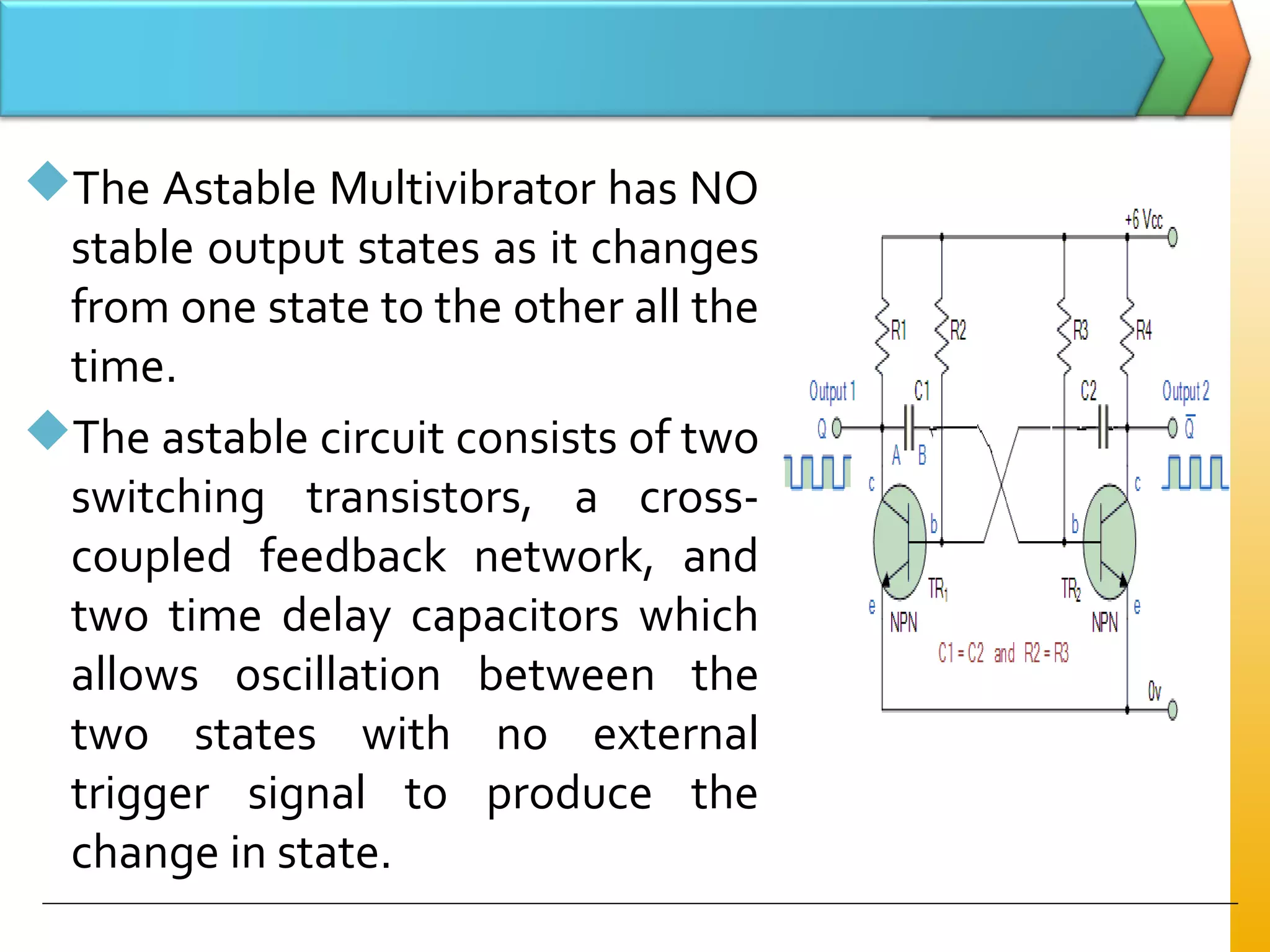

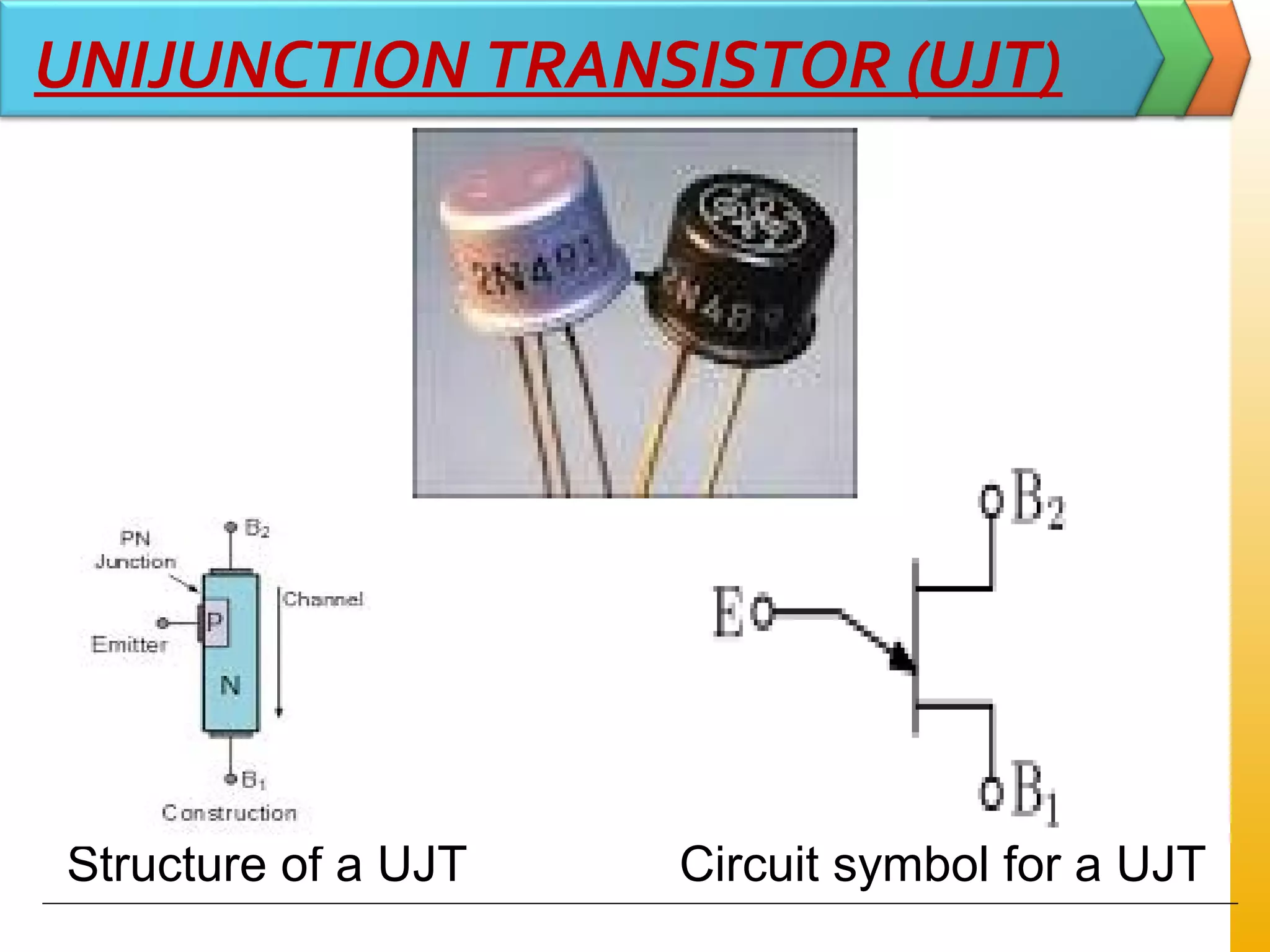

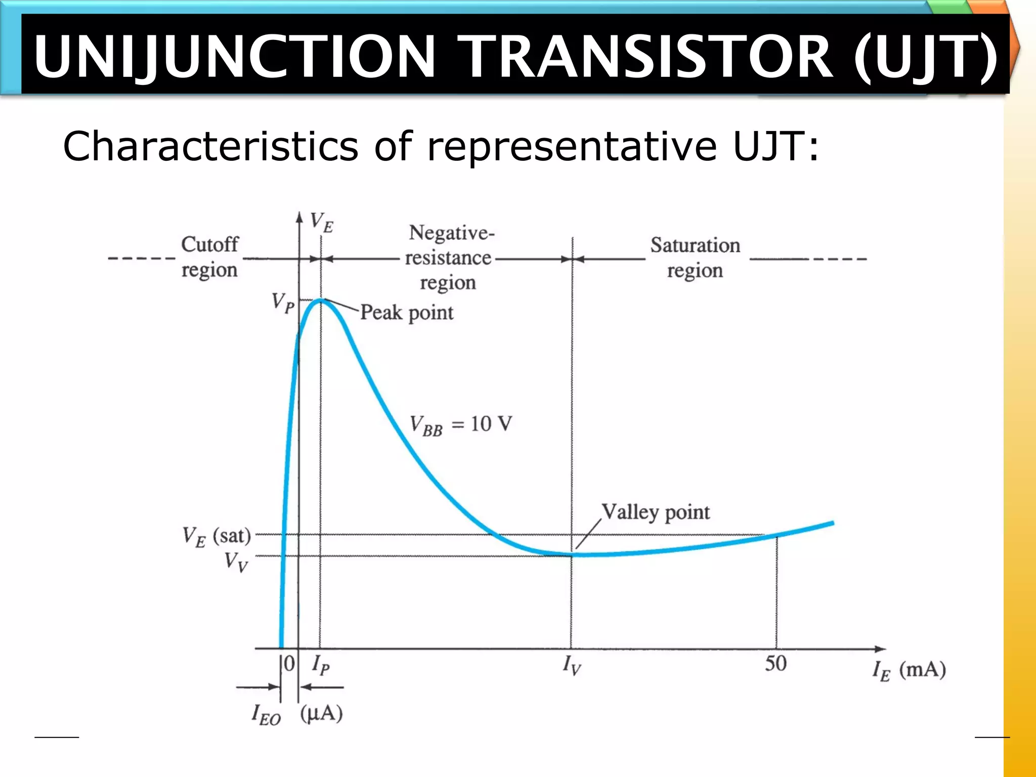

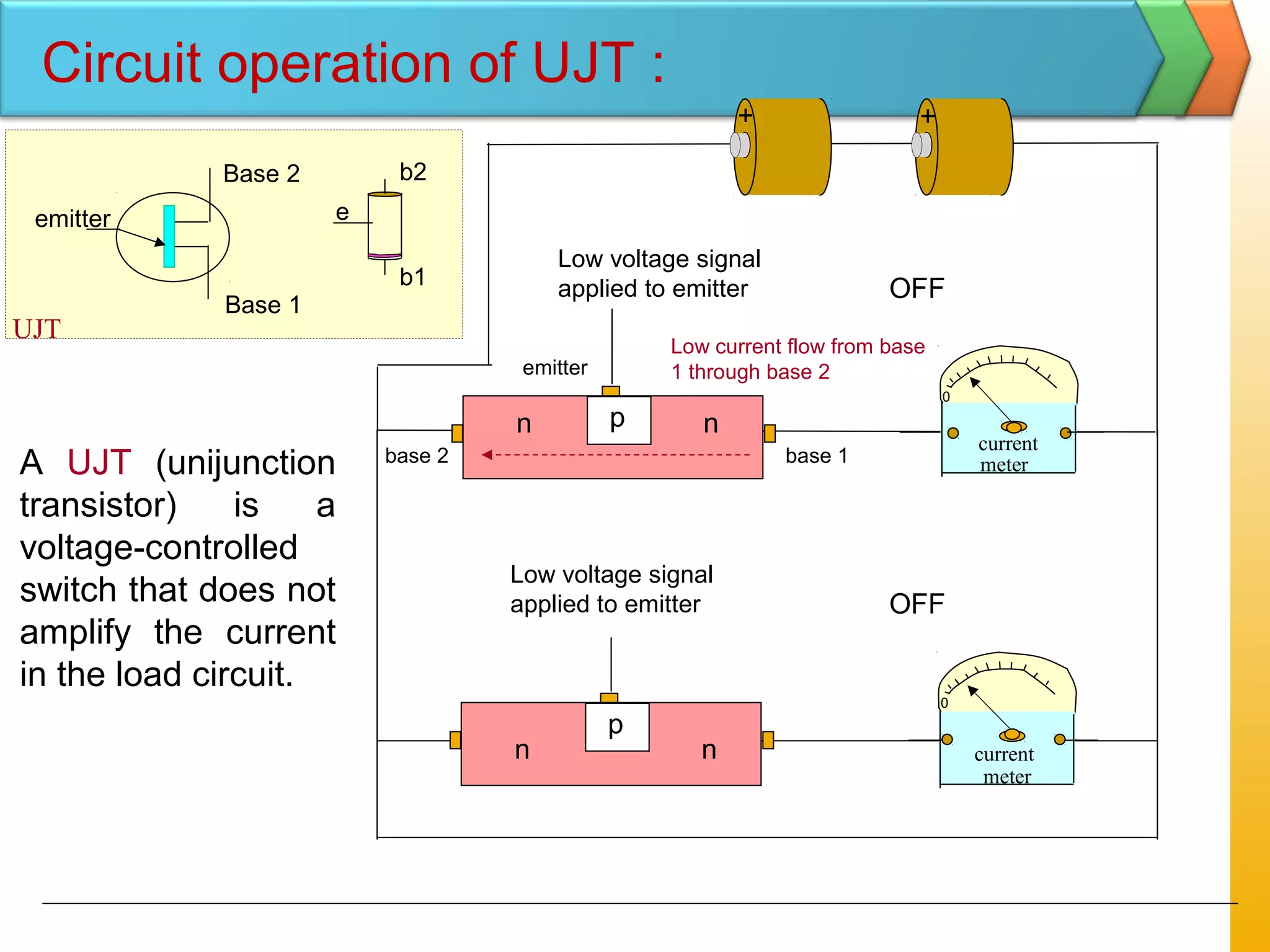
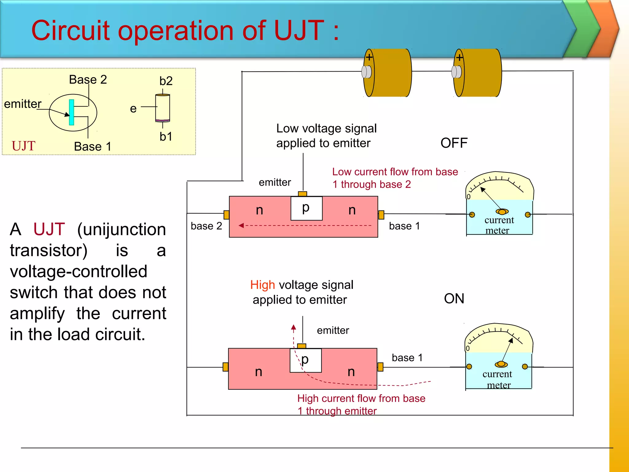
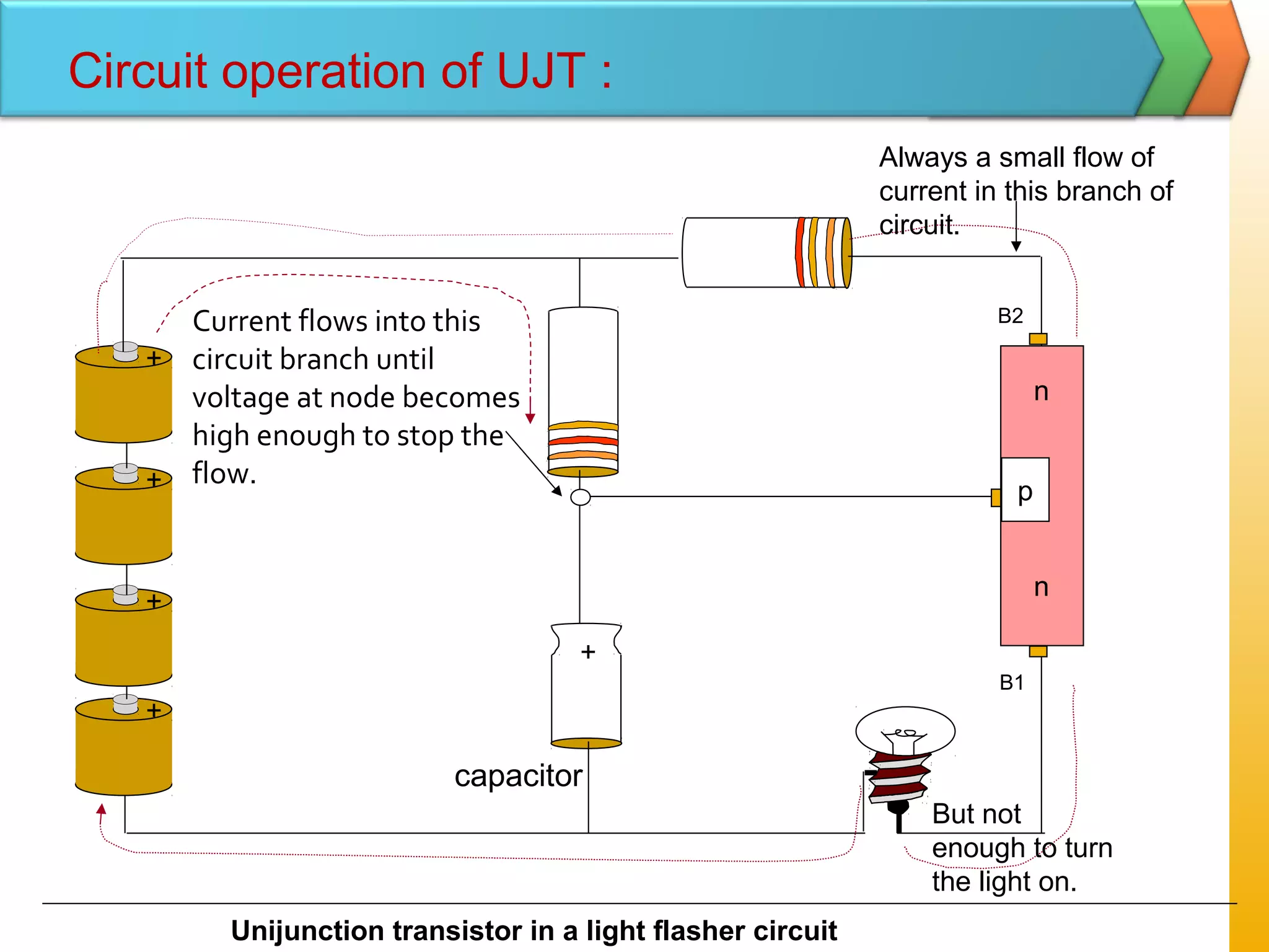
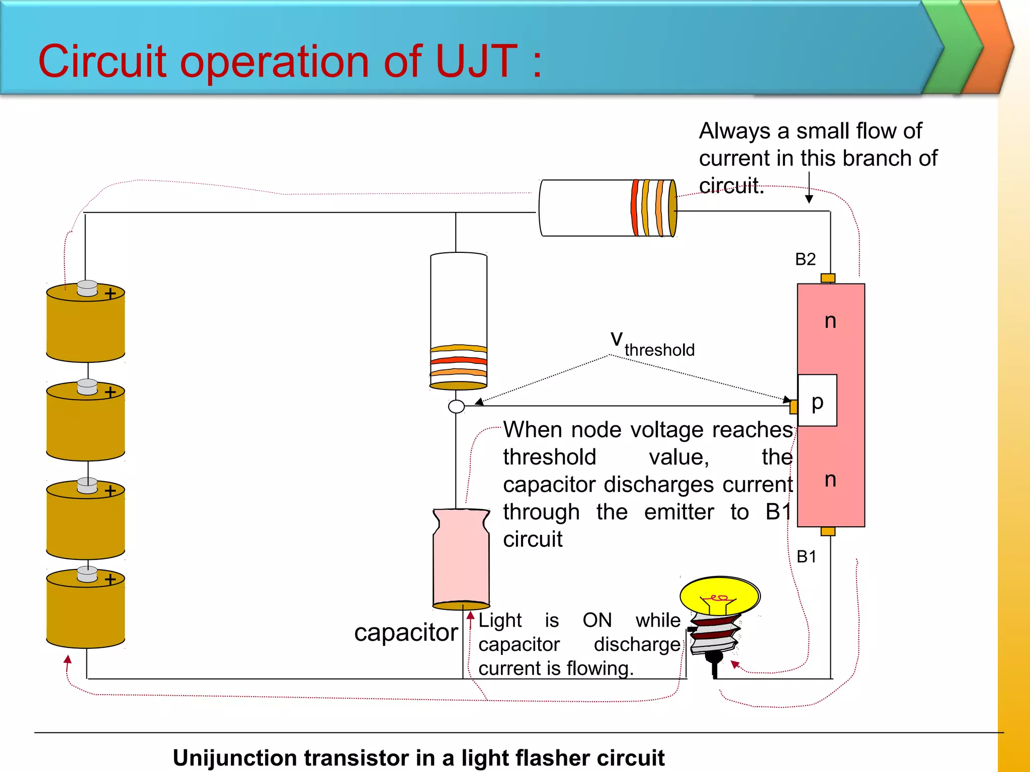
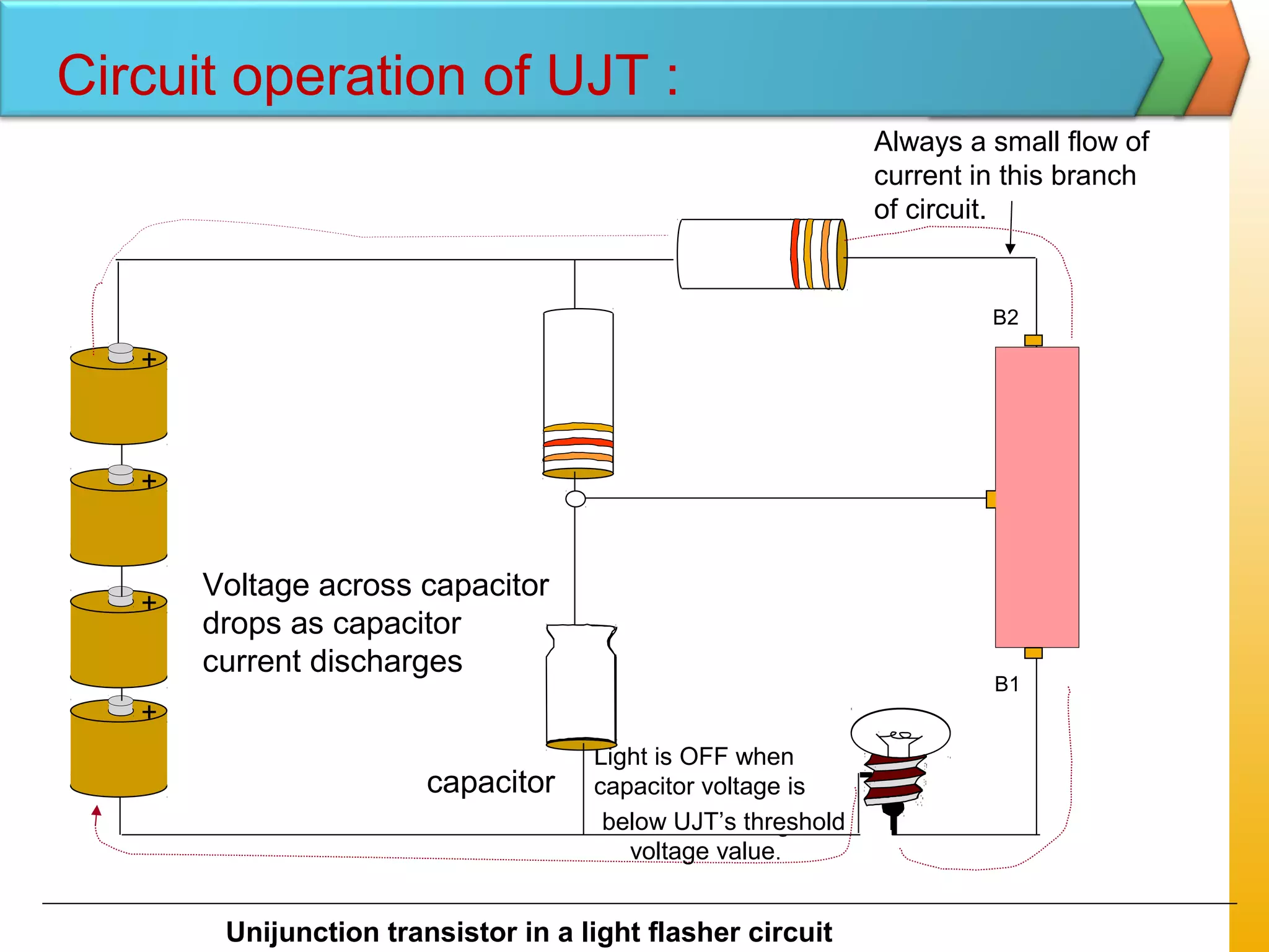
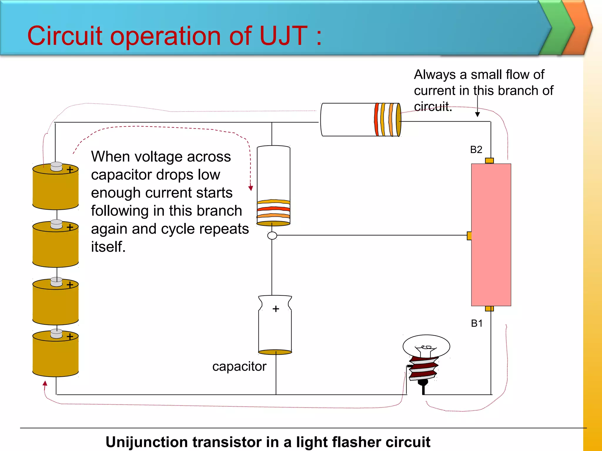
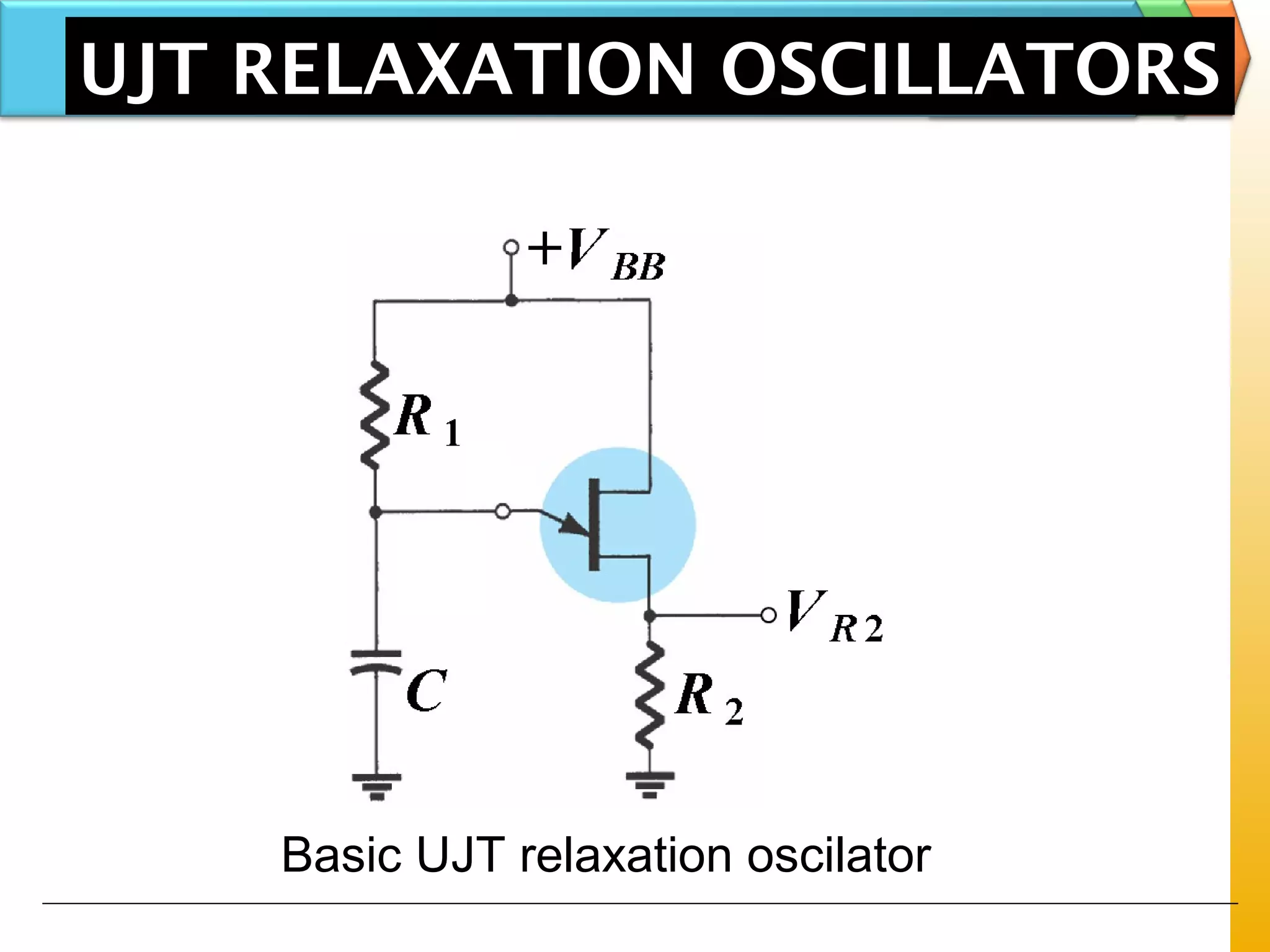
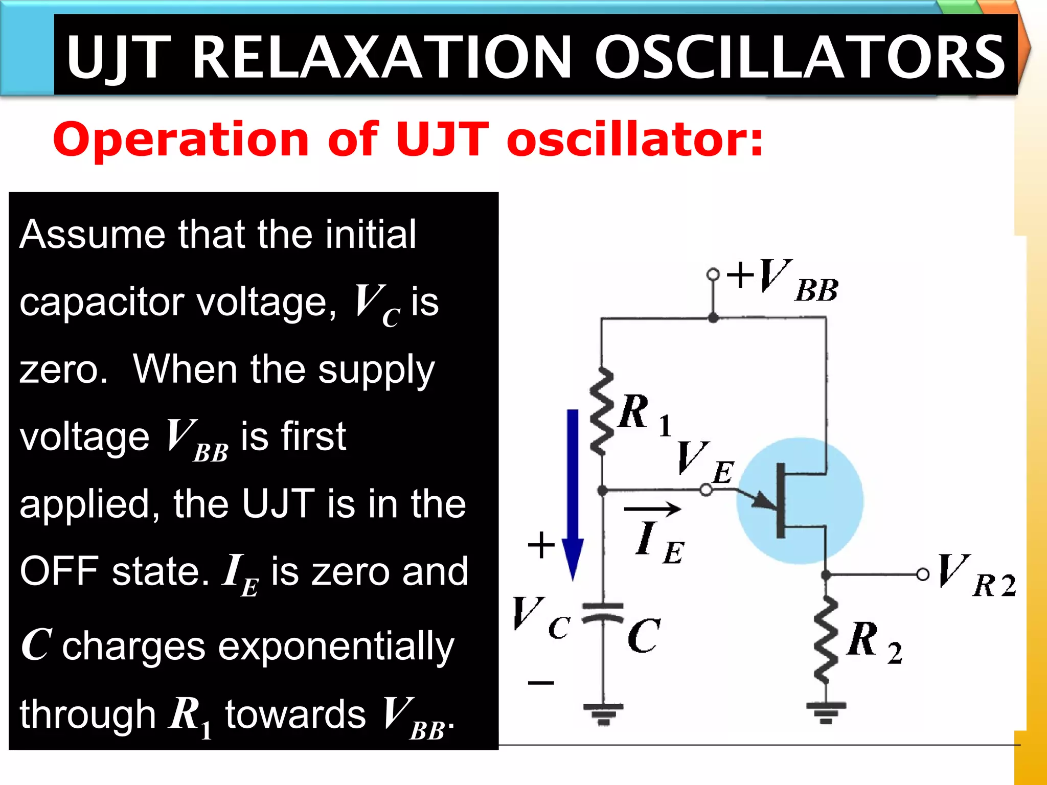
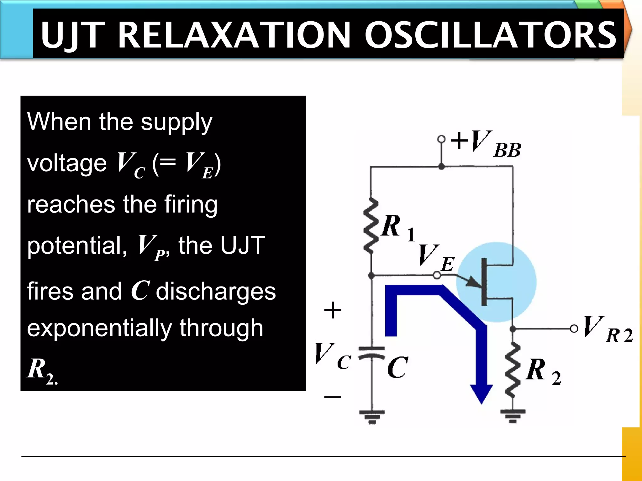

This document discusses different types of multivibrators and unijunction transistors (UJTs). It describes astable, monostable, and bistable multivibrators. Astable multivibrators continuously switch between two states to produce a square wave without any input trigger. Monostable multivibrators have one stable state and switch to a transient state upon a trigger, then return to the stable state after a set time. Bistable multivibrators have two stable states and switch between them with an external trigger. The document also discusses UJTs, including their structure, characteristics, and use in relaxation oscillator circuits such as a light flasher.


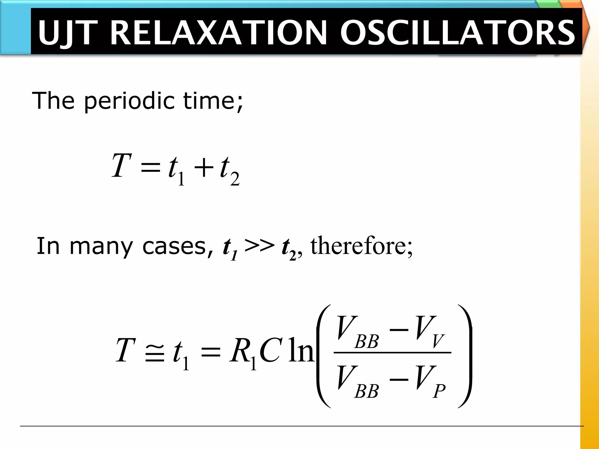
![RF Circuit Design - [Ch2-1] Resonator and Impedance Matching](https://cdn.slidesharecdn.com/ss_thumbnails/ch2-1-150613064353-lva1-app6892-thumbnail.jpg?width=640&height=640&fit=bounds)


