Downloaded 503 times

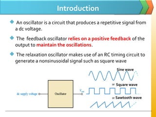
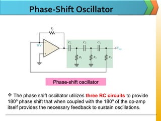
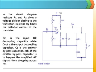
![Phase-Shift Oscillator
Loop gain, T(s):
Set s=jw
3
2
1
)()()(
+
==
sRC
sRC
R
R
ssAsT β
[ ] [ ]222222
2
2
3
2
331
))((
)(
1
)(
CRRCjCR
RCRCj
R
R
jT
RCj
RCj
R
R
jT
ωωω
ωω
ω
ω
ω
ω
−+−
−=
+
=](https://image.slidesharecdn.com/sinusoidaloscillators-141231041844-conversion-gate02/85/Sinusoidal-oscillators-36-320.jpg)
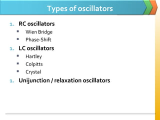
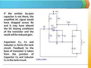
![Phase-Shift Oscillator
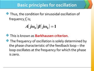
To satisfy condition T(jwo)=1, real component must
be zero since the numerator is purely imaginary.
the oscillation frequency:
Apply wo in equation:
To satisfy condition T(jwo)=1
031 222
=− CRω
RC3
1
0 =ω
[ ]
−=
−+
−=
8
1
)3/1(3)3/(0
)3/1)(3/(
)( 22
R
R
j
j
R
R
jT oω
82
=
R
R The gain greater than 8, the circuit will
spontaneously begin oscillating & sustain
oscillations](https://image.slidesharecdn.com/sinusoidaloscillators-141231041844-conversion-gate02/85/Sinusoidal-oscillators-37-320.jpg)

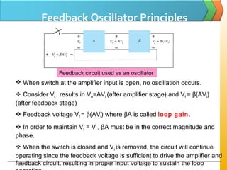
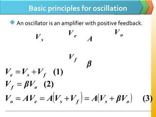
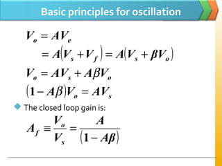
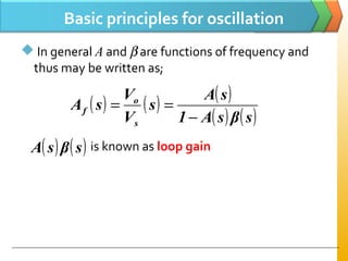
The document provides an overview of oscillators, detailing their basic concepts, types, and principles of operation, including RC, LC, and relaxation oscillators. It emphasizes feedback mechanisms necessary for sustaining oscillations, outlines design criteria, and presents specific examples like the Wien-bridge and phase-shift oscillators. Additionally, the document explains the role of components such as capacitors and resistors in determining the frequency and stability of various oscillator configurations.


