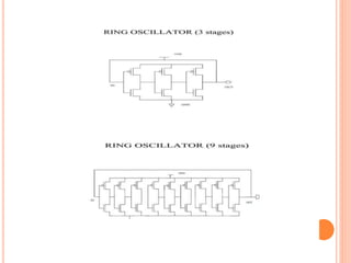
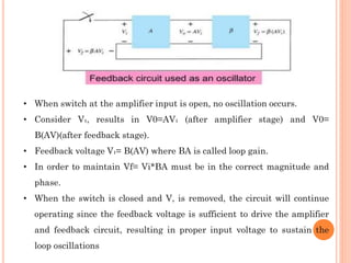
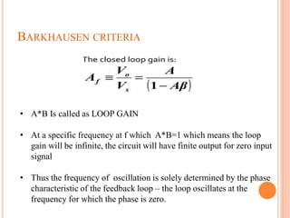
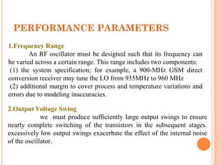
An oscillator is an electronic circuit that generates a periodic waveform without an external signal source. It relies on positive feedback to maintain oscillations. There are two main types - the feedback oscillator which uses positive feedback of the output, and the relaxation oscillator which uses an RC timing circuit to generate a non-sinusoidal signal like a square wave. For an oscillator to operate, the loop gain of the feedback must be at least 1, and the phase must be zero, at a specific oscillation frequency determined by the phase characteristics of the feedback loop. Key parameters for oscillator performance include frequency range, output voltage swing, drive capability, phase noise, and power dissipation. A ring oscillator uses an odd number of inverter stages in a closed
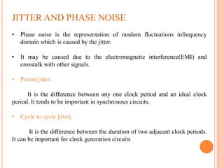
![3. Drive Capability
The LO must drive the input Capacitance of at least one mixer and
one divider[frequency synthesizer].
4.Phase Noise
The spectrum of an oscillator in practice deviates from an impulse
and is “broadened” by the noise of its constituent devices. Called “phase noise,”
this phenomenon has a profound effect on RF receivers and transmitters. Since
the phase noise of LC oscillators is inversely proportional to the Q of their tank,
we will pay particular attention to factors that degrade the Q.
5.Power Dissipation
The power drained by the LO and its buffers proves critical in some
applications as it trades with the phase noise and tuning range. Thus, many
techniques have been introduced that lower the phase noise for a given power
dissipation](https://image.slidesharecdn.com/oscilators-230510031402-1416060a/85/OSCILATORS-introduction-ring-oscillator-6-320.jpg)