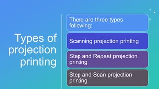
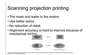
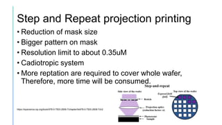
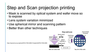
Projection lithography uses an optical system to focus and project a mask image onto a silicon wafer. There are three main types: scanning projection which moves the mask and wafer, step and repeat which replicates a larger mask pattern across the wafer, and step and scan which scans the mask while moving the wafer. Projection lithography allows for higher resolution than contact lithography without damaging masks. It enables mass production of integrated circuits with feature sizes below 100nm.


![Thin_Film_Technology_introduction[1]](https://cdn.slidesharecdn.com/ss_thumbnails/1b4496c8-2102-411b-8465-a3dd3f398327-150205034538-conversion-gate02-thumbnail.jpg?width=640&height=640&fit=bounds)


