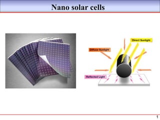
Nano solar cells


                   1
Contents


• Introduction

• Solar cells

• Solar product availability

• Thin film materials

• Cadmium Telluride solar cells

• CIGS solar cells

• CIGS manufacturing process

• Nanosolar

• Conclusion


                                          2
What is a Solar Cell

•   A device that converts solar energy directly to electricity by the photovoltaic
    effect

     – It supplies voltage and current to a

        resistive load (light, battery, motor)

     – It supplies DC power

•   Solar Module or Solar Panel

     – Solar Module: Solar cells are wired in series

     – Solar Panel: Solar Modules are assembled together and placed into a frame


                                                                                      3
Photovoltaic Solar Cells
Generate electricity directly from sunlight

 2 Main types:

 Single-crystal silicon (traditional)
                                                     Silicon-based solar
          • Widespread                               cell

          • Expensive to manufacture

 Dye-sensitized (“nano”)

          • Newer, less proven

          • Inexpensive to manufacture

          • Flexible
                                                     Dye-sensitized
                                                     solar cell


                                                                       4
Current Technology: Photovoltaic Cells


Short Version: Light in, electricity out.
•   If the energy of the incident photons equals or exceeds the band gap energy of the
    material, then the valence electrons will get excited, and enter the conduction band.
•   They are susceptible to an electric field and form electricity.


                                                                                            5
…But Not All Energy is Converted…
•   Like chloroplasts in plants, solar cells can only absorb specific wavelengths of
    light.

•   In both, light that isn‟t absorbed is either transmitted through or reflected back.

•   Whether a certain wavelength of lights gets absorbed depends on its energy.


                                                 Chlorophyll molecules absorb
                                                 blue and red light, but reflect
                                                 green light


                                                                                          6
Nanotechnology To The Rescue
•   Chemists at the University of California, Berkeley, have designed a „plastic‟
    solar cell which utilizes tiny nanorods to convert light into electricity

•   These solar cells consist of a layer of tiny nanorods only 200 nanometers thick,
    dispersed within a polymer.

•   So far these cells can produce only 0.7 volts, so they are only appropriate for
    low-power devices.

•   These cells could be mass produced because the nanorod layers could simply
    be applied in separate coats.


                                                                                       7
•   Nanorods behave as wires because when they absorb light of a specific wavelength
    they generate electrons.
•   These electrons flow through the nanorods until they reach the aluminum electrode
    where they are combined to form a current and are used as electricity.
This type of cell is cheaper to manufacture than conventional ones for two main reasons.
     •    Plastic cells are not made from silicon, which can be very expensive.
     •    Manufacturing these cells does not require expensive equipment like
          conventional silicon based solar cells.


                                                                                           8
How a Dye-Sensitized Cell Works


•   Light with high enough energy excites electrons in dye molecules.
•   Excited electrons infused into semiconducting TiO2, transported out of cell
•   Positive “holes” left in dye molecules
•   Separation of excited electrons and “holes” creates a voltage


                                                                                  9
Solar product availability


                             10
Thin film solar cells


•   Made     by    depositing     one   or     more    thin   layers       (thin   film)
    of photovoltaic material on a substrate.

•   A thin film of semiconductor is deposited by low cost methods

•   Less material is required

•   Cells can be flexible and integrated directly into roofing material.

•   Categorized based on the material used

     – Amorphous silicon (a-Si) and other thin-film silicon (TF-Si)

     – Cadmium telluride (CdTe)

     – Copper indium gallium selenide (CIS or CIGS)

     – Dye-sensitized solar cell (DSC)


                                                                                           11
Sources of energy loss
                           Thermalization of excess
                           energy
Efficiency limits                    CB
                                  Below band gap photons
                                  not absorbed
                                    VB


                                                      12
Advantages of thin films


• Efficient and high performing materials
   – Direct bandgap semiconductors
   – Better energy output –kWh/KW
   – CIGS record at 20%+ conversion efficiency
• Significantly reduced costs
   – Less material usage
   – Not affected by silicon supply shortages
   – Potential for improving costs throughout value chain
• Advanced manufacturing techniques
   – Fewer processing steps
   – Monolithic integration of circuits
   – Automation
• Better aesthetics


                                                            13
Comparison of materials

Technology     Maximum          Advantages          Disadvantages
              Demonstrate
              d Efficiency
             for small cells
   a-Si          12.2%            Mature            Low efficiency
                               manufacturing     High equipment costs
                                technology
  CdTe           16.5%           Low-cost         Medium efficiency
                               manufacturing      Rigid glass substrate
  CIGS           19.9%         High efficiency Film uniformity challenge
                               Glass or flexible   on large substrates
                                  substrates


                                                                           14
Cadmium Telluride (CdTe) Solar Cells

                                                       glass


                                            CdS/CdTe
•   Direct bandgap, Eg=1.45eV
•   High efficiency (Record:16.5%;
    Industry: 11%)
•   High module production speed
•   Long term stability (20 years)
                                                               15
Disadvantages of Cadmium Telluride


• Cadmium is toxic

• Tellurium is a limited reserve
    – First Solar used half of the world‟s annual production of Te in
      2009

    – The cost of Te could go up a lot before affecting the price of solar
      cells

Search for other abundant materials…


                                                                             16
CIGS solar cells


CIGS - Copper Indium Gallium (di)Selenide
•   The material is a solid solution of copper indium selenide (1.0 eV)
    and copper gallium selenide (1.7 eV )

•   Because the material strongly absorbs sunlight, a much thinner film is required
    than of other semiconductor materials. The CIGS absorber is deposited on a
    glass backing, along with electrodes to collect current

•   CIGS solar cells has efficiencies greater than 20% as compared to 10% for
    silicon based solar cell


                                                                                      17
CIGS solar cells


         Shell Solar, CA
         Global Solar Energy, AZ
         Energy Photovoltaics, NJ
         ISET, CA
         ITN/ES, CO
         NanoSolar Inc., CA
         DayStar Technologies, NY/CA
         MiaSole, CA
         HelioVolt, Tx
         Solyndra, CA
         SoloPower, CA

         Wurth Solar, CIS Solartechnik and
         Solarion, Germany
         Solibro, Sweden
         CISEL, France
         Showa Shell and Honda, Japan
         Mosar Baer and Rays Expert, India

                                             18
CIGS manufacturing process


• The most common vacuum-based process co-
  sputters CIG, then anneals the resulting film
  with a selenide vapor to form the final CIGS
  structure.
• NanoSolar uses a non-vacuum-based process
  that mixes the materials into a liquid then
  deposits nano-particles of the precursor
  materials on the substrate and then sinters it.
• SoloPower uses electroplating to apply the
  CIGS layer.
• Another technique is to dissolve the material
  into a liquid, apply it to a surface and bake it.


                                                      19
Nanosolar


            20
Solar Farms


              21
Future of Nano solar cells


• There is huge demand for use of renewable resources due to its low
   carbon footprint with solar energy is leading the race as a viable
   alternative for fossil fuels

• Low efficiency and expensive silicon wafers, makes nano solar cells
   the future of solar panels

• Along with silicon and CIGS, other materials are being studied which
   produce higher efficiencies and at a low cost


                                                                         22
PV Solutions for Urban Solarcells
          Future of Nano solar Applications


                                              23
Commercial flat roof (attached & ballasted)


                                              24
Pitched roof (tiles & rack mount)


                                    25
Covered parking


                  26
Covered areas (walkways, outdoor Cafés, etc..)


                                                 27
Sunshades


            28
Balance of Systems(Mounting, wiring, inverters, etc.)


                                                        29
Thank You


            30
References
•   http://www.utexas.edu/pmcs/sustainability/documents/UTHelioVoltPresentati
    on.pdf
•   http://www.youtube.com/watch?v=EYy0beorZHk
•   http://www.stanford.edu/group/mcgehee/presentations.html


                                                                                31
CIGS manufacturing process


                             32

Nano solar cells

  • 1.
  • 2.
    Contents • Introduction • Solarcells • Solar product availability • Thin film materials • Cadmium Telluride solar cells • CIGS solar cells • CIGS manufacturing process • Nanosolar • Conclusion 2
  • 3.
    What is aSolar Cell • A device that converts solar energy directly to electricity by the photovoltaic effect – It supplies voltage and current to a resistive load (light, battery, motor) – It supplies DC power • Solar Module or Solar Panel – Solar Module: Solar cells are wired in series – Solar Panel: Solar Modules are assembled together and placed into a frame 3
  • 4.
    Photovoltaic Solar Cells Generateelectricity directly from sunlight  2 Main types:  Single-crystal silicon (traditional) Silicon-based solar • Widespread cell • Expensive to manufacture  Dye-sensitized (“nano”) • Newer, less proven • Inexpensive to manufacture • Flexible Dye-sensitized solar cell 4
  • 5.
    Current Technology: PhotovoltaicCells Short Version: Light in, electricity out. • If the energy of the incident photons equals or exceeds the band gap energy of the material, then the valence electrons will get excited, and enter the conduction band. • They are susceptible to an electric field and form electricity. 5
  • 6.
    …But Not AllEnergy is Converted… • Like chloroplasts in plants, solar cells can only absorb specific wavelengths of light. • In both, light that isn‟t absorbed is either transmitted through or reflected back. • Whether a certain wavelength of lights gets absorbed depends on its energy. Chlorophyll molecules absorb blue and red light, but reflect green light 6
  • 7.
    Nanotechnology To TheRescue • Chemists at the University of California, Berkeley, have designed a „plastic‟ solar cell which utilizes tiny nanorods to convert light into electricity • These solar cells consist of a layer of tiny nanorods only 200 nanometers thick, dispersed within a polymer. • So far these cells can produce only 0.7 volts, so they are only appropriate for low-power devices. • These cells could be mass produced because the nanorod layers could simply be applied in separate coats. 7
  • 8.
    Nanorods behave as wires because when they absorb light of a specific wavelength they generate electrons. • These electrons flow through the nanorods until they reach the aluminum electrode where they are combined to form a current and are used as electricity. This type of cell is cheaper to manufacture than conventional ones for two main reasons. • Plastic cells are not made from silicon, which can be very expensive. • Manufacturing these cells does not require expensive equipment like conventional silicon based solar cells. 8
  • 9.
    How a Dye-SensitizedCell Works • Light with high enough energy excites electrons in dye molecules. • Excited electrons infused into semiconducting TiO2, transported out of cell • Positive “holes” left in dye molecules • Separation of excited electrons and “holes” creates a voltage 9
  • 10.
  • 11.
    Thin film solarcells • Made by depositing one or more thin layers (thin film) of photovoltaic material on a substrate. • A thin film of semiconductor is deposited by low cost methods • Less material is required • Cells can be flexible and integrated directly into roofing material. • Categorized based on the material used – Amorphous silicon (a-Si) and other thin-film silicon (TF-Si) – Cadmium telluride (CdTe) – Copper indium gallium selenide (CIS or CIGS) – Dye-sensitized solar cell (DSC) 11
  • 12.
    Sources of energyloss Thermalization of excess energy Efficiency limits CB Below band gap photons not absorbed VB 12
  • 13.
    Advantages of thinfilms • Efficient and high performing materials – Direct bandgap semiconductors – Better energy output –kWh/KW – CIGS record at 20%+ conversion efficiency • Significantly reduced costs – Less material usage – Not affected by silicon supply shortages – Potential for improving costs throughout value chain • Advanced manufacturing techniques – Fewer processing steps – Monolithic integration of circuits – Automation • Better aesthetics 13
  • 14.
    Comparison of materials Technology Maximum Advantages Disadvantages Demonstrate d Efficiency for small cells a-Si 12.2% Mature Low efficiency manufacturing High equipment costs technology CdTe 16.5% Low-cost Medium efficiency manufacturing Rigid glass substrate CIGS 19.9% High efficiency Film uniformity challenge Glass or flexible on large substrates substrates 14
  • 15.
    Cadmium Telluride (CdTe)Solar Cells glass CdS/CdTe • Direct bandgap, Eg=1.45eV • High efficiency (Record:16.5%; Industry: 11%) • High module production speed • Long term stability (20 years) 15
  • 16.
    Disadvantages of CadmiumTelluride • Cadmium is toxic • Tellurium is a limited reserve – First Solar used half of the world‟s annual production of Te in 2009 – The cost of Te could go up a lot before affecting the price of solar cells Search for other abundant materials… 16
  • 17.
    CIGS solar cells CIGS- Copper Indium Gallium (di)Selenide • The material is a solid solution of copper indium selenide (1.0 eV) and copper gallium selenide (1.7 eV ) • Because the material strongly absorbs sunlight, a much thinner film is required than of other semiconductor materials. The CIGS absorber is deposited on a glass backing, along with electrodes to collect current • CIGS solar cells has efficiencies greater than 20% as compared to 10% for silicon based solar cell 17
  • 18.
    CIGS solar cells Shell Solar, CA Global Solar Energy, AZ Energy Photovoltaics, NJ ISET, CA ITN/ES, CO NanoSolar Inc., CA DayStar Technologies, NY/CA MiaSole, CA HelioVolt, Tx Solyndra, CA SoloPower, CA Wurth Solar, CIS Solartechnik and Solarion, Germany Solibro, Sweden CISEL, France Showa Shell and Honda, Japan Mosar Baer and Rays Expert, India 18
  • 19.
    CIGS manufacturing process •The most common vacuum-based process co- sputters CIG, then anneals the resulting film with a selenide vapor to form the final CIGS structure. • NanoSolar uses a non-vacuum-based process that mixes the materials into a liquid then deposits nano-particles of the precursor materials on the substrate and then sinters it. • SoloPower uses electroplating to apply the CIGS layer. • Another technique is to dissolve the material into a liquid, apply it to a surface and bake it. 19
  • 20.
  • 21.
  • 22.
    Future of Nanosolar cells • There is huge demand for use of renewable resources due to its low carbon footprint with solar energy is leading the race as a viable alternative for fossil fuels • Low efficiency and expensive silicon wafers, makes nano solar cells the future of solar panels • Along with silicon and CIGS, other materials are being studied which produce higher efficiencies and at a low cost 22
  • 23.
    PV Solutions forUrban Solarcells Future of Nano solar Applications 23
  • 24.
    Commercial flat roof(attached & ballasted) 24
  • 25.
    Pitched roof (tiles& rack mount) 25
  • 26.
  • 27.
    Covered areas (walkways,outdoor Cafés, etc..) 27
  • 28.
  • 29.
    Balance of Systems(Mounting,wiring, inverters, etc.) 29
  • 30.
  • 31.
    References • http://www.utexas.edu/pmcs/sustainability/documents/UTHelioVoltPresentati on.pdf • http://www.youtube.com/watch?v=EYy0beorZHk • http://www.stanford.edu/group/mcgehee/presentations.html 31
  • 32.

Editor's Notes

  • #15 Silicon wafers are 150 µm thick, the wafers demand multiple processing steps before they can be integrated into a module. On the contrary, thin-film solar cells utilize only a 1-4 µm-thick layer of semiconducting material to produce electricity, thus requiring less processing and fewer materials.
  • #19 World record efficiency = 20.0 %.Many companies are evaporating, printing, sputtering and electro-depositing it.Handling a 4-element compound is tough.
  • #20 Sputering: Atoms are ejected from a solid due to bombardment of energetic particlesSintering: Creating objects from powders
  • #33 TCO - transparent conductive oxideIn chemistry, a precursor is a compound that participates in the chemical reaction that produces another compound.