Download as PDF, PPTX
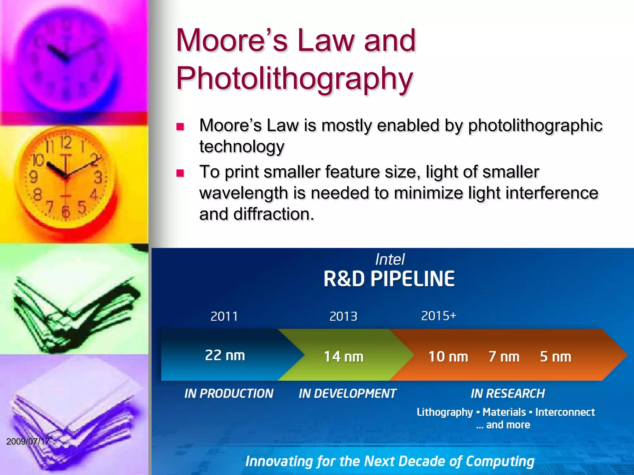


This document discusses advanced photolithography technologies used to enable Moore's Law. Moore's Law allows the number of transistors on integrated circuits to double every two years by reducing transistor size. To print smaller features, light with smaller wavelengths is needed to minimize diffraction. Technologies discussed to improve resolution for smaller wavelengths include optical proximity correction, off-axis illumination, phase shift masks, double patterning, restricted design rules, and negative tone development. These resolution enhancement techniques allow continued transistor scaling below 60nm feature sizes.
Presentation by Dr. Len Mei discussing advanced semiconductor photolithographic technologies.
Moore's Law relates to photolithography, requiring smaller wavelength light for enhanced resolutions.
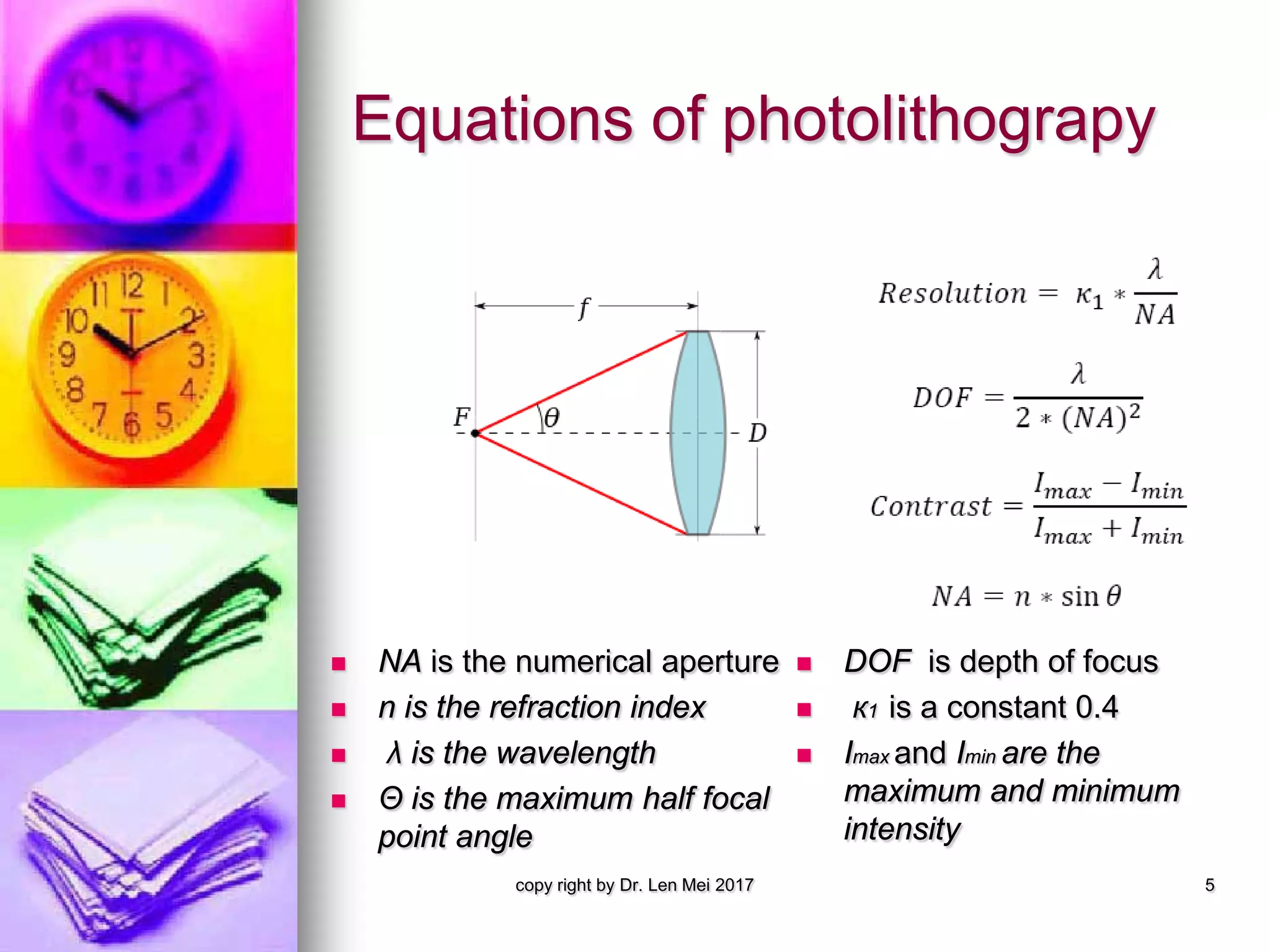
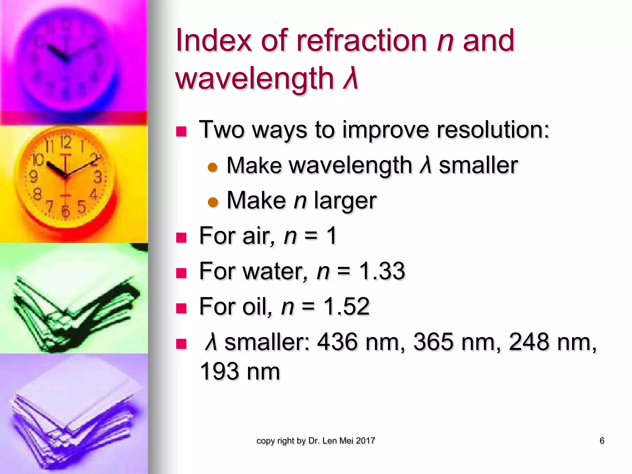
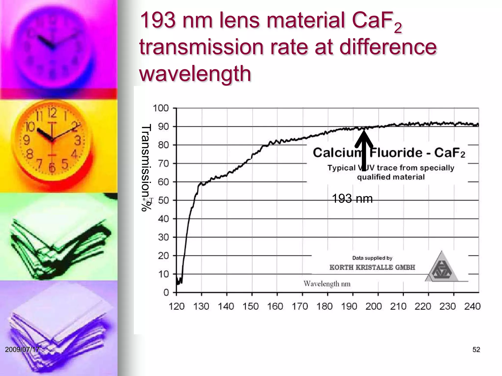
Key equations in photolithography to improve resolution via numerical aperture, refraction index, and wavelength reductions.
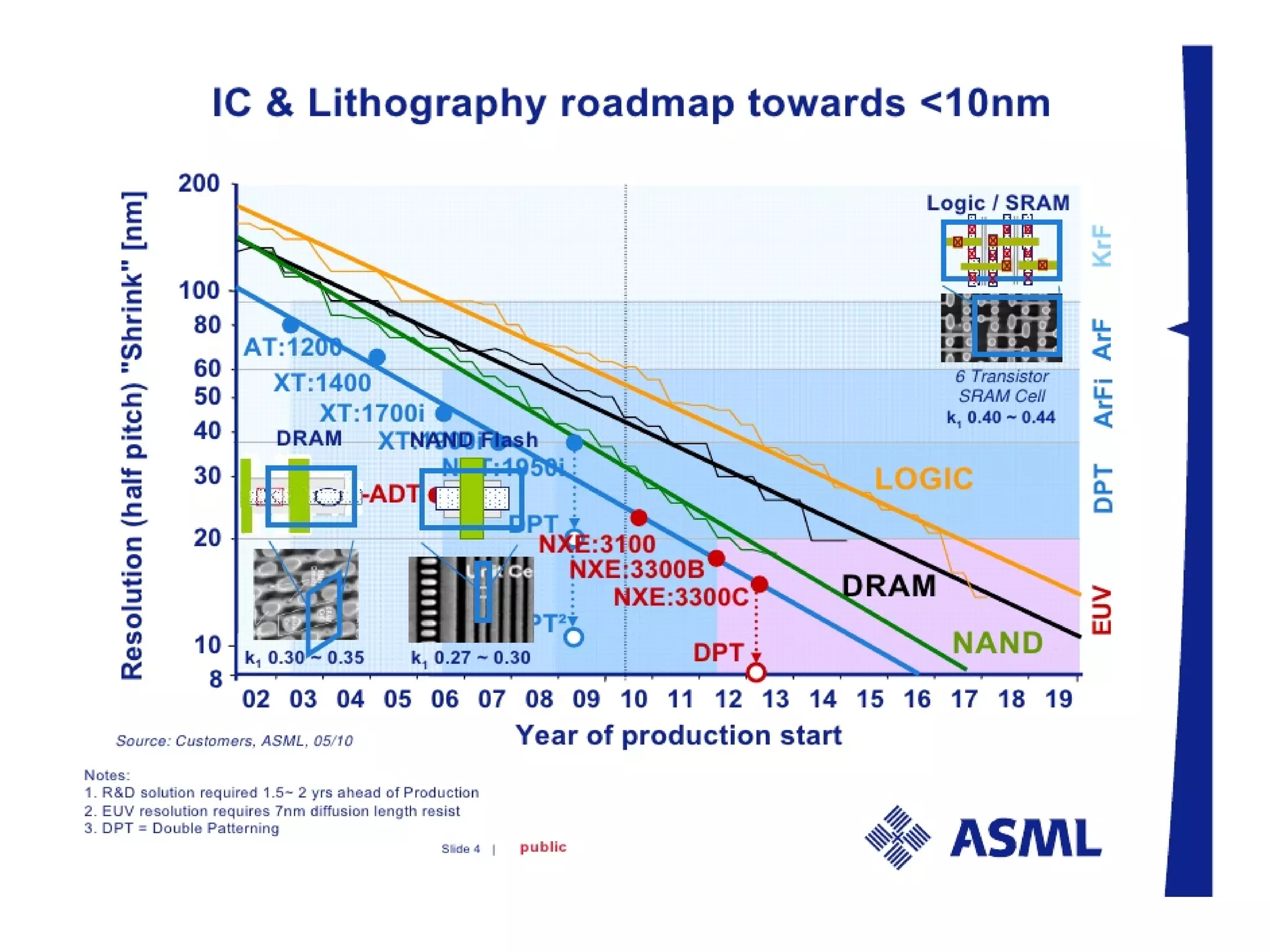
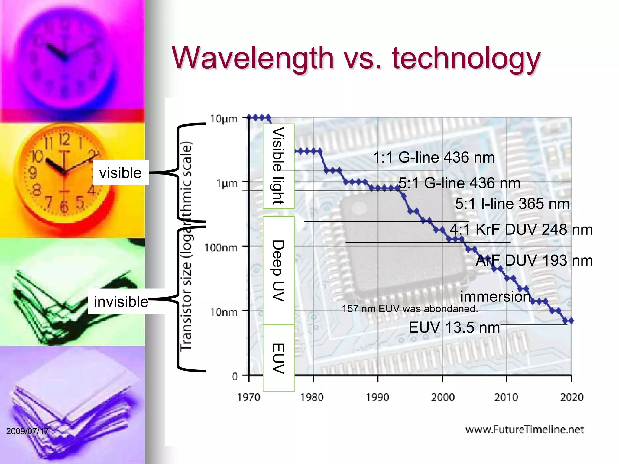
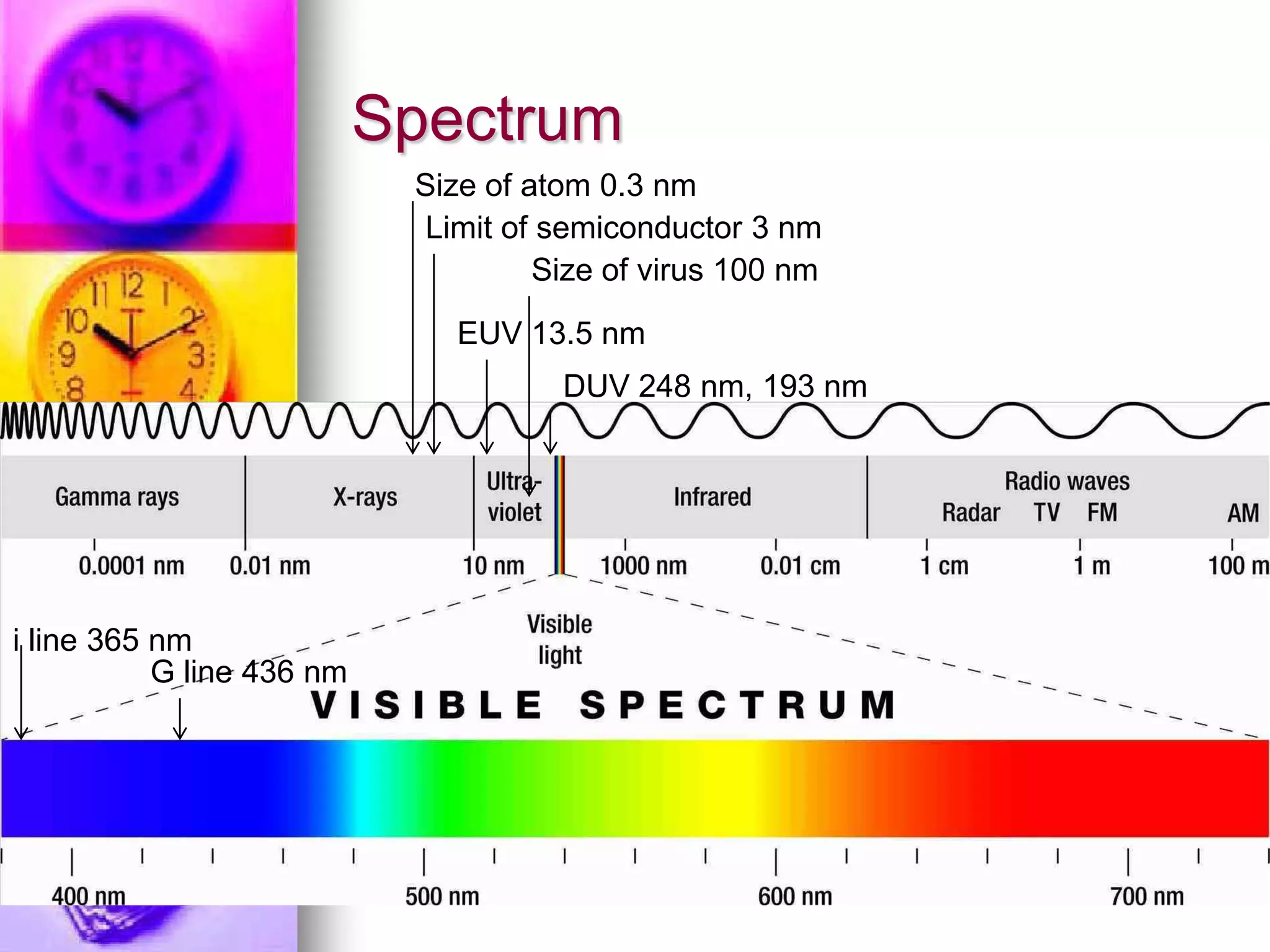
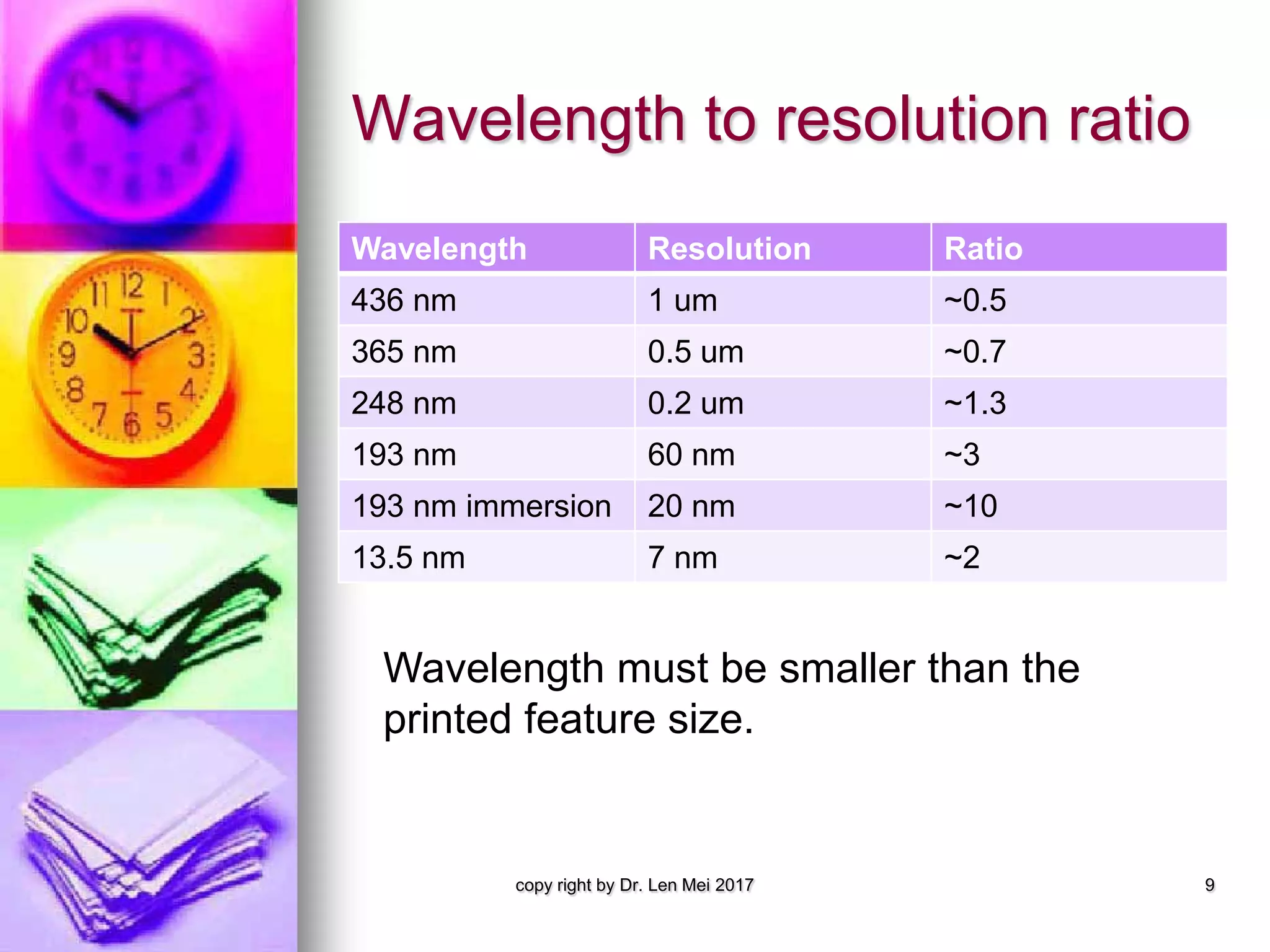
Comparison of lithographic technologies by wavelength, detailing resolutions achievable as wavelengths decrease.
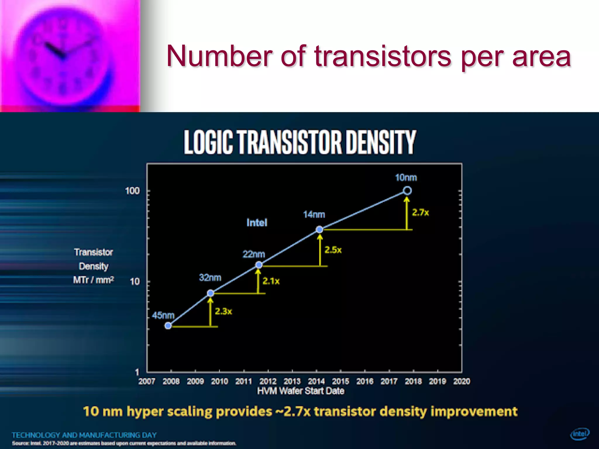
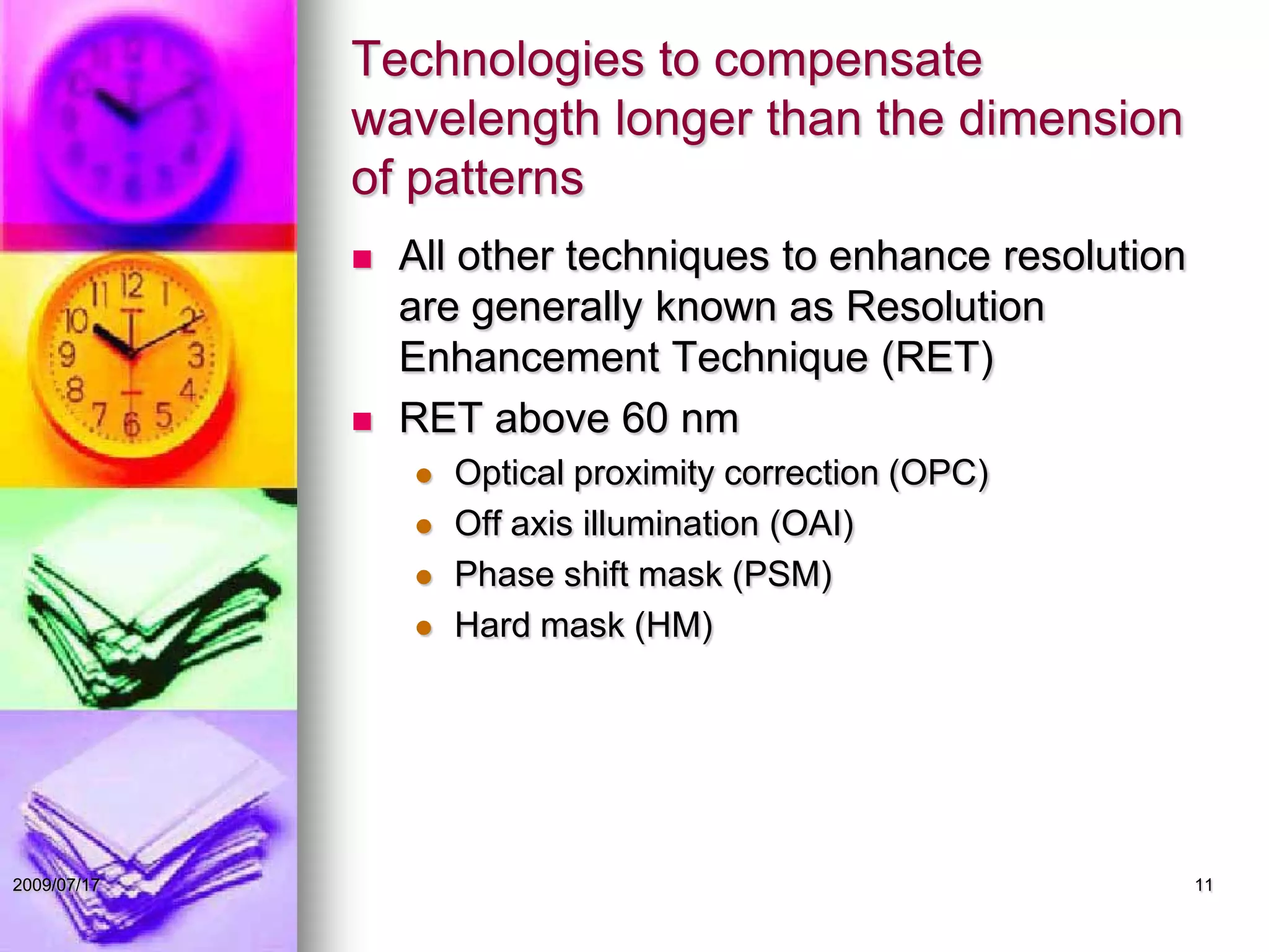
Overview of advancements in photolithography technology, including resolution enhancement techniques for patterns larger than 60 nm.
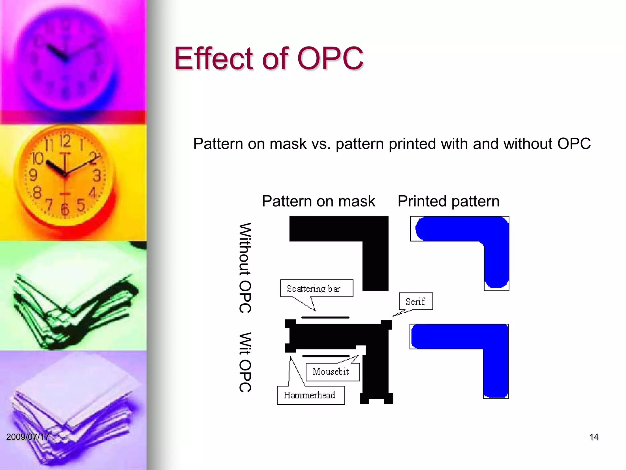
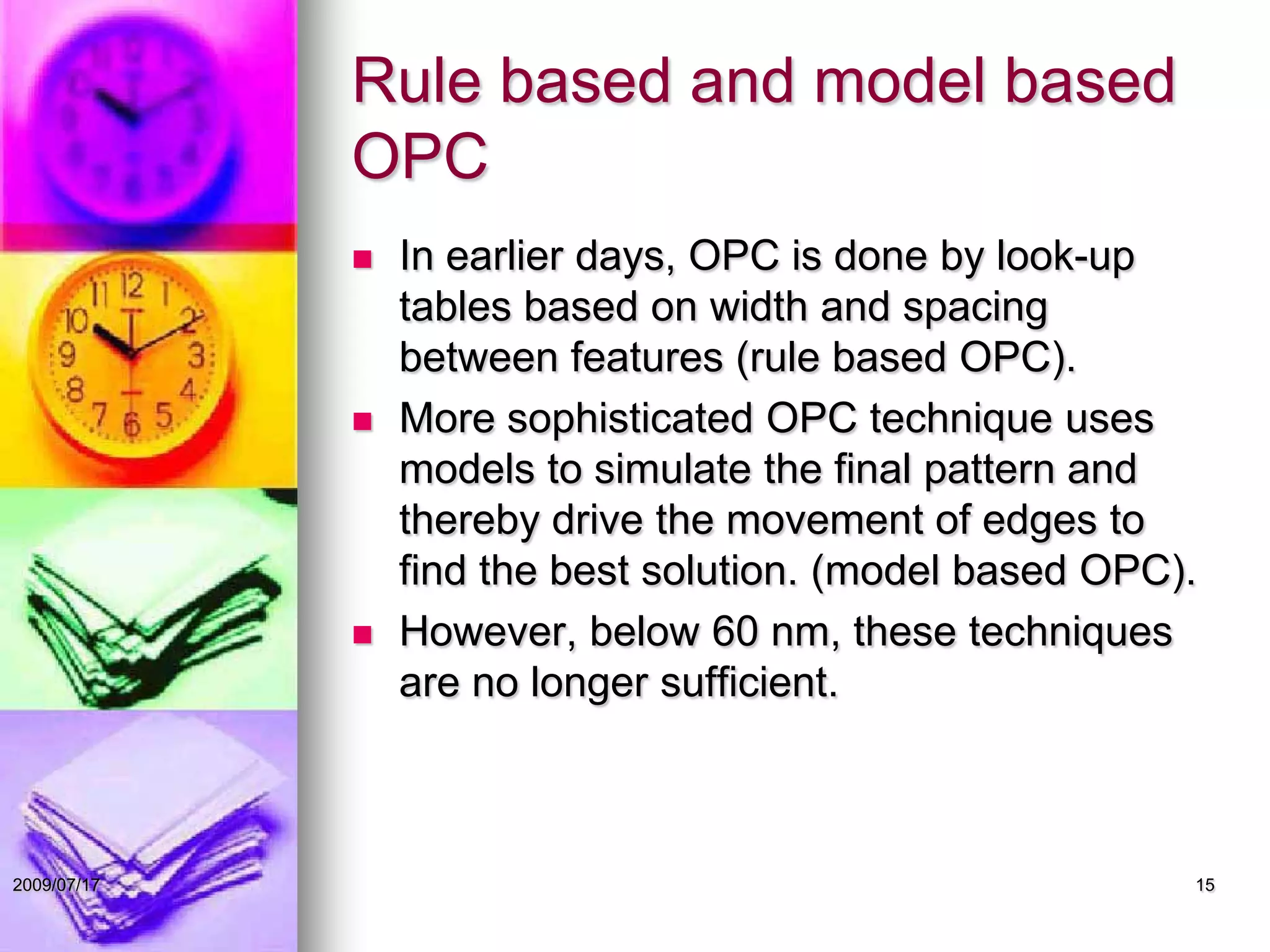
OPC techniques correct imaging errors from diffraction; includes rule-based and model-based approaches.
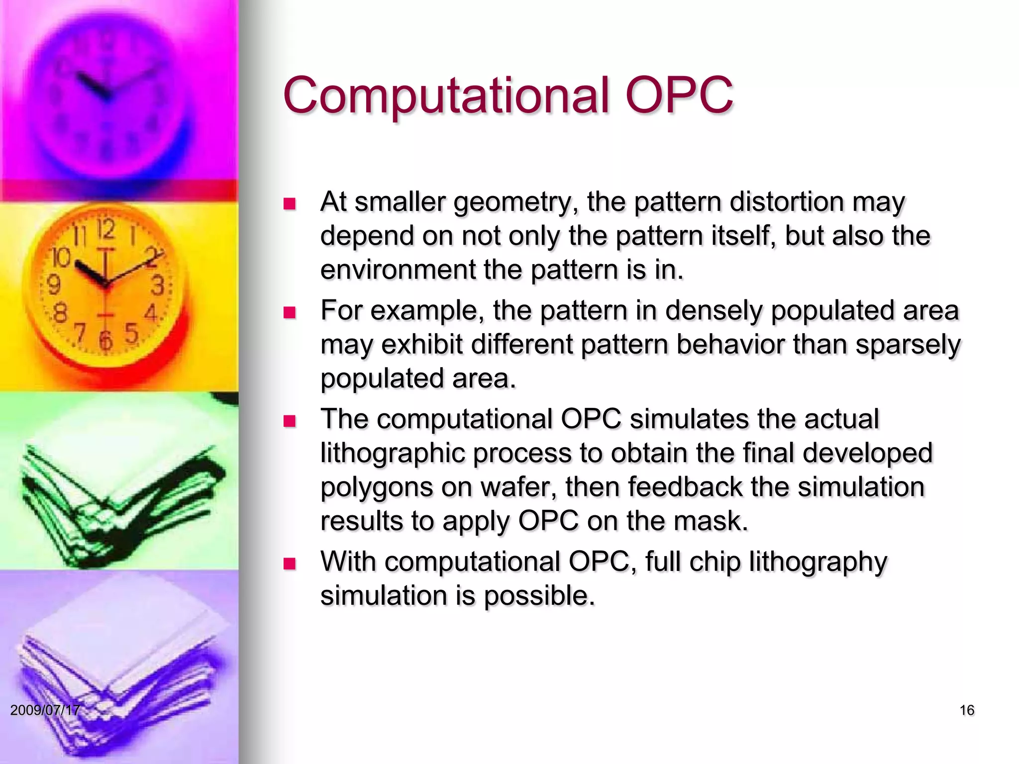
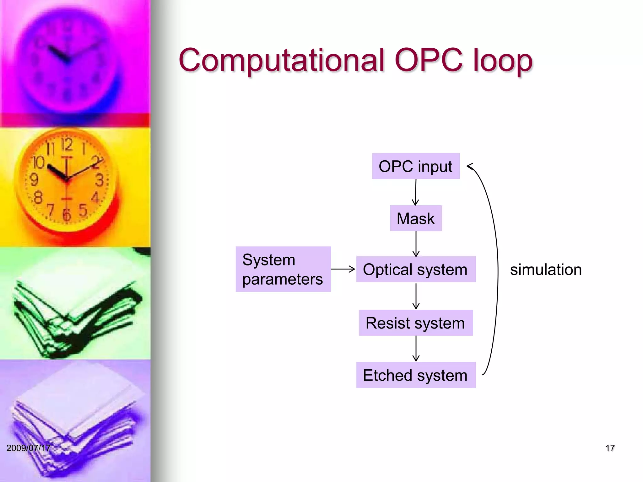
Computational OPC simulates lithographic processes for enhanced patterning, factoring site density effects.
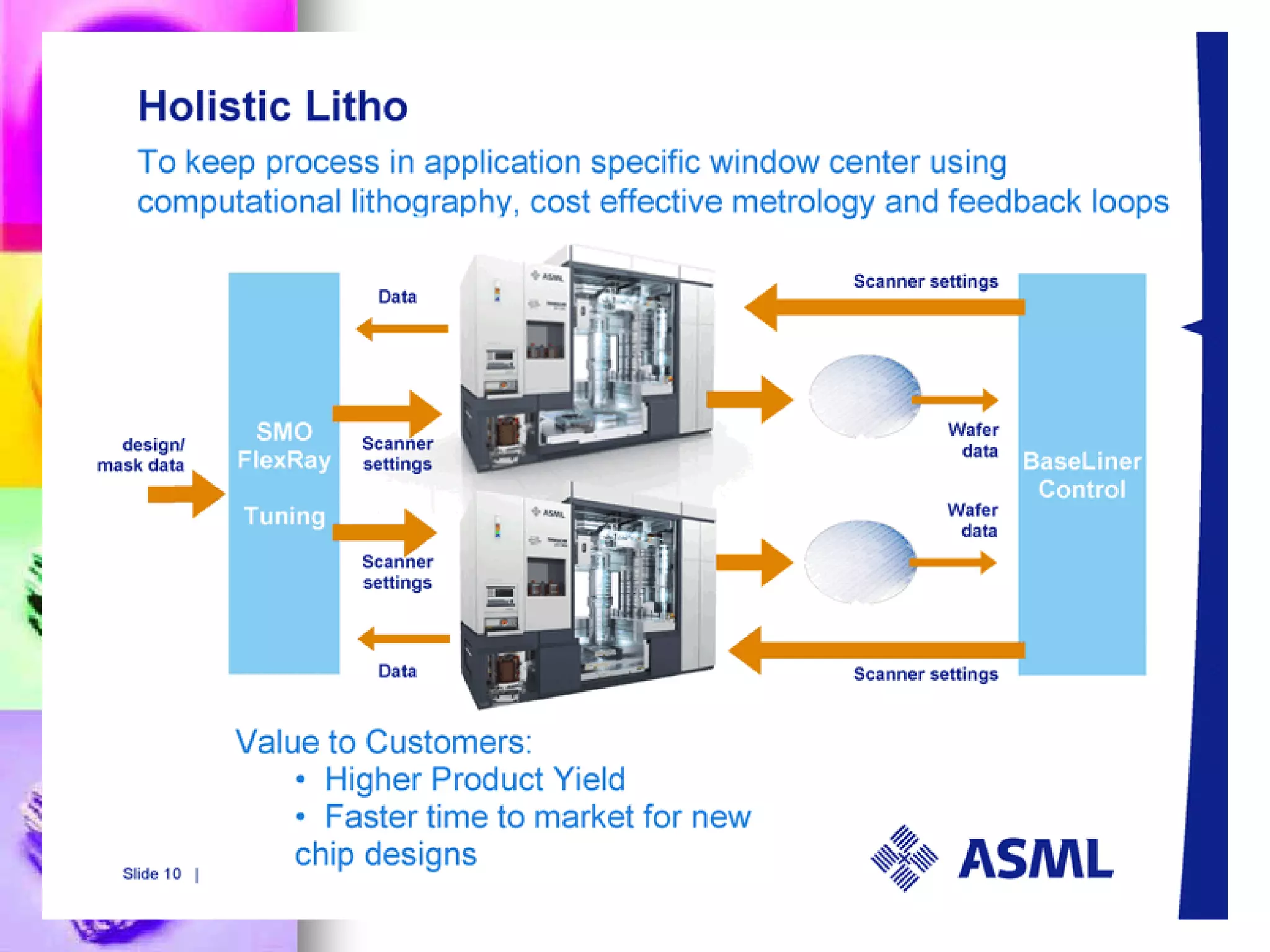
SMO is a computational approach enhancing lithographic capabilities by optimizing mask patterns and illumination.
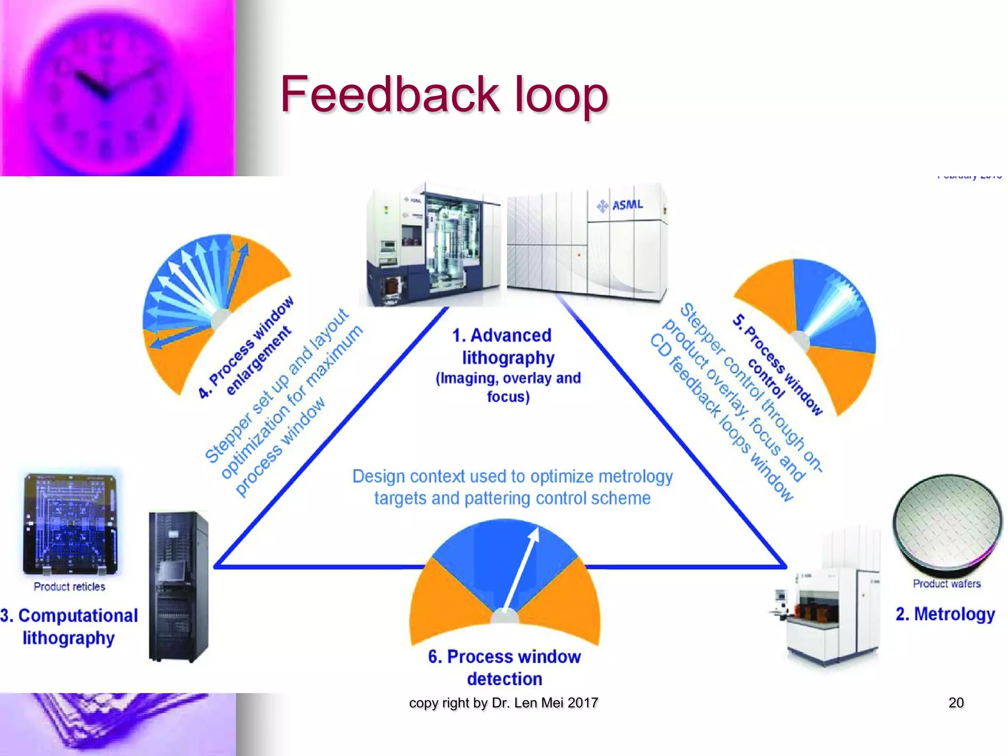
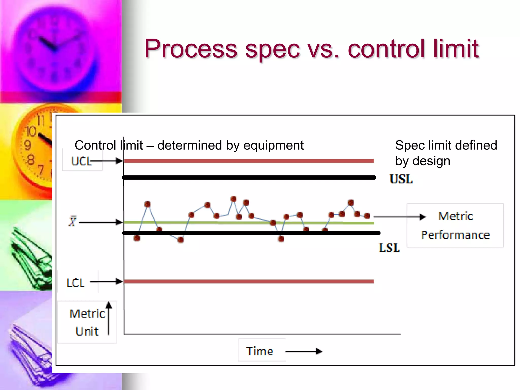
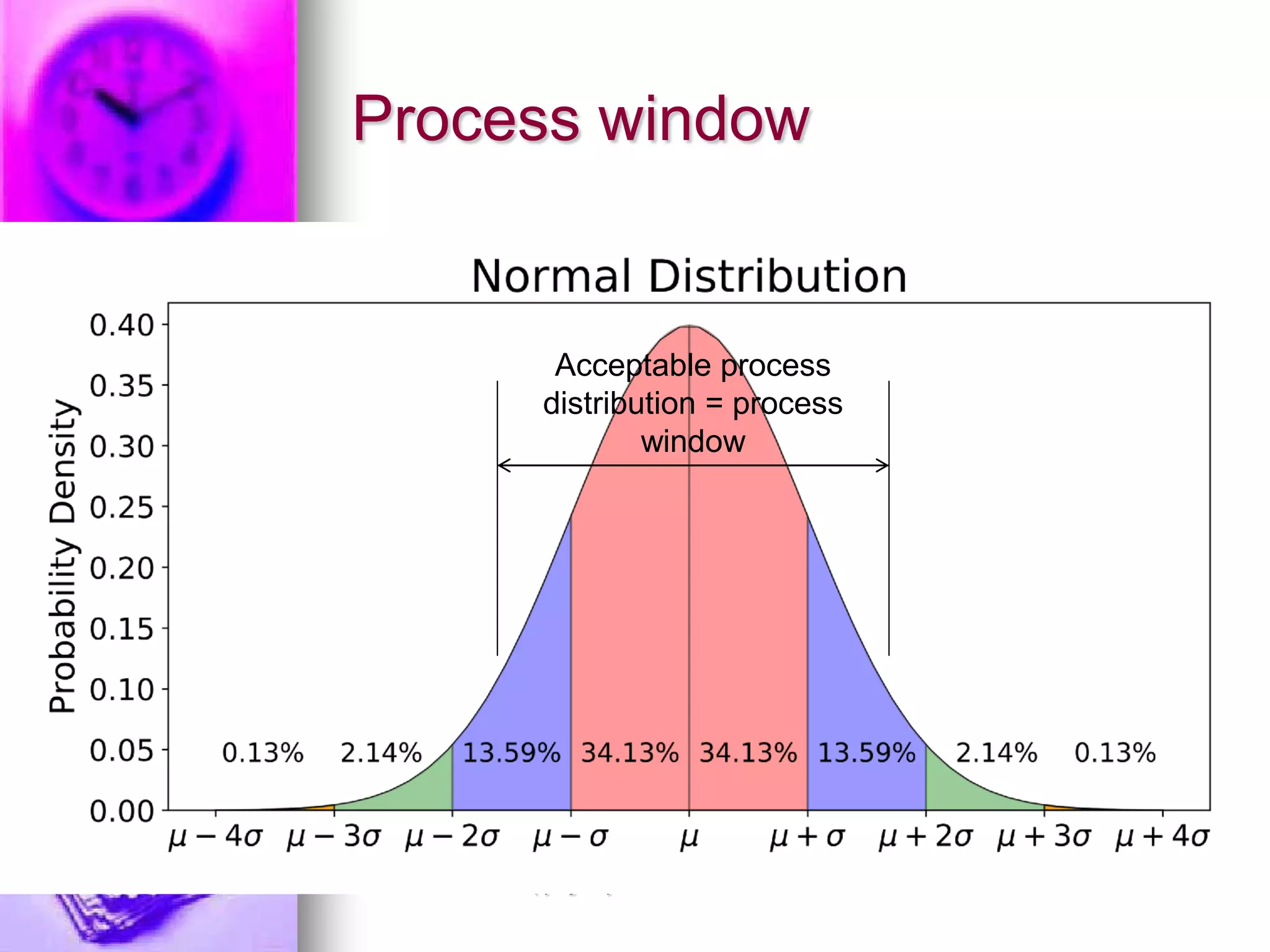
Process specifications vs. control limits; a robust process window is vital for effective lithography.
Inverse Lithography Technology designs masks by simulating the desired wafer patterns and correcting variations.
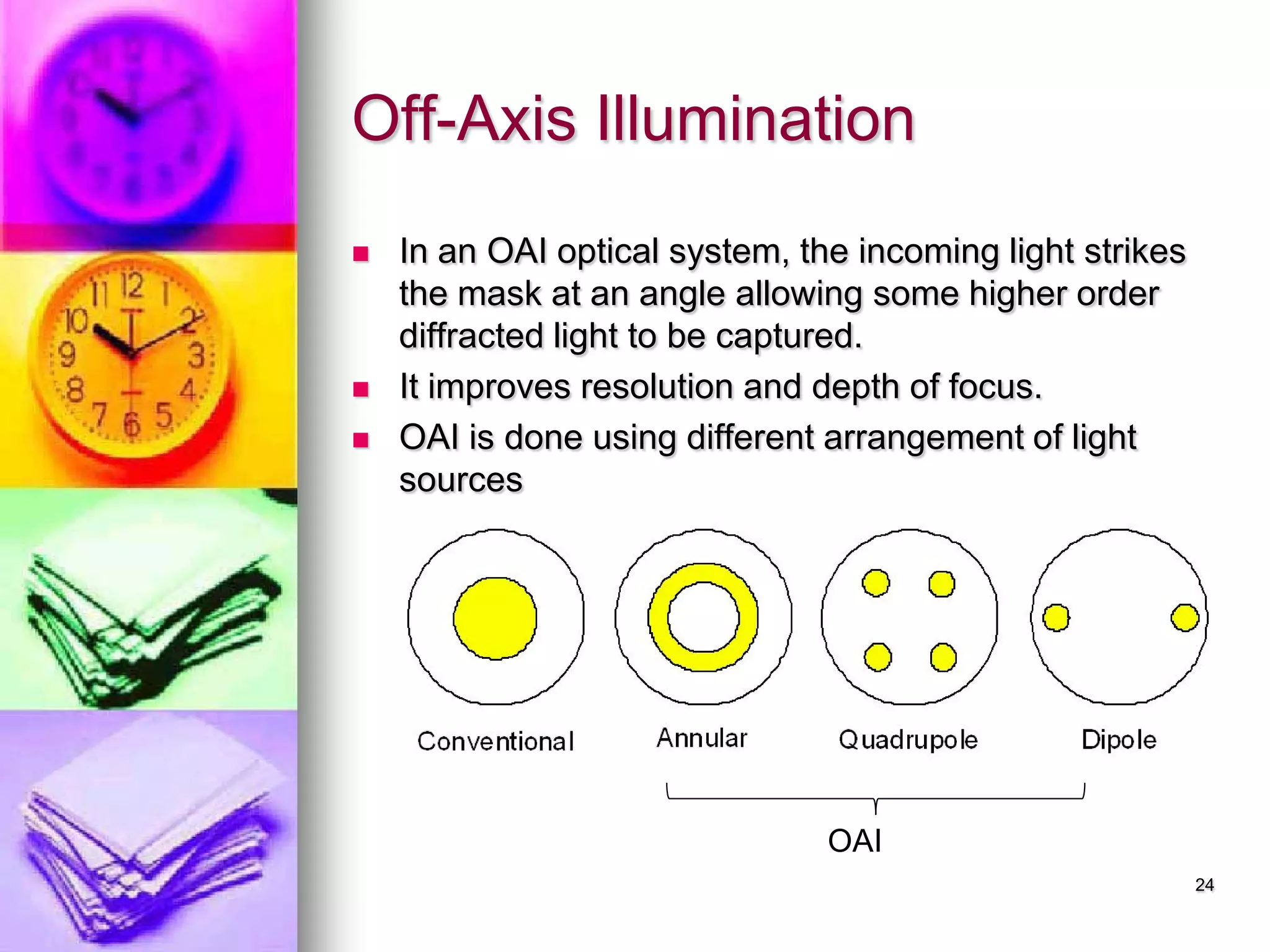
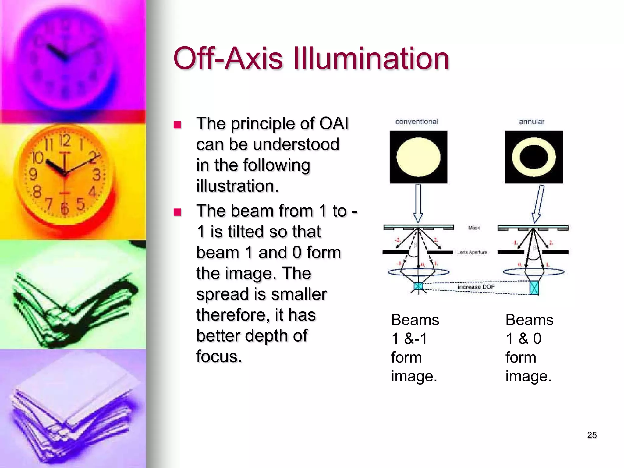
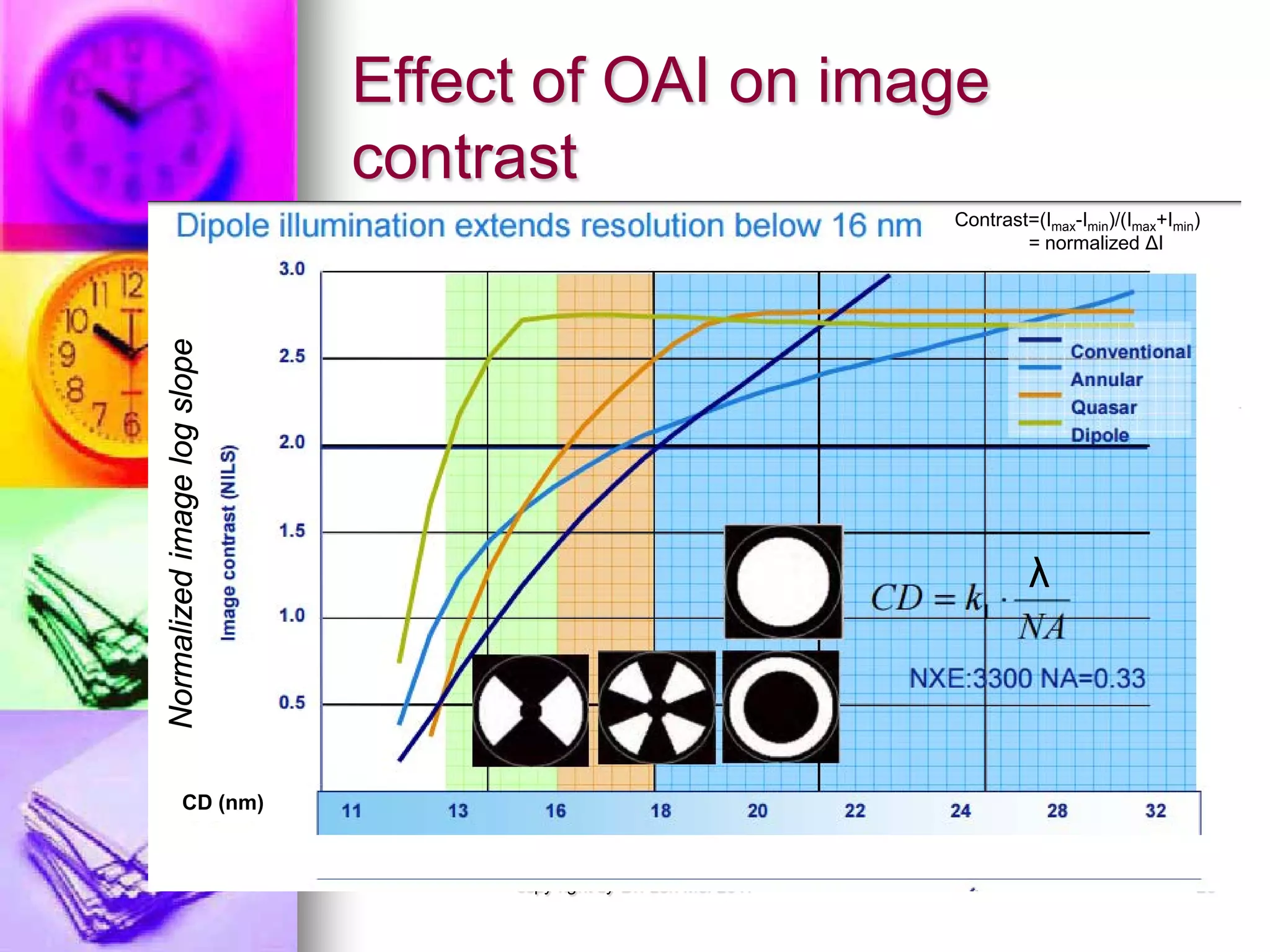
OAI techniques enhance resolution by allowing light to interact with masks at different angles.
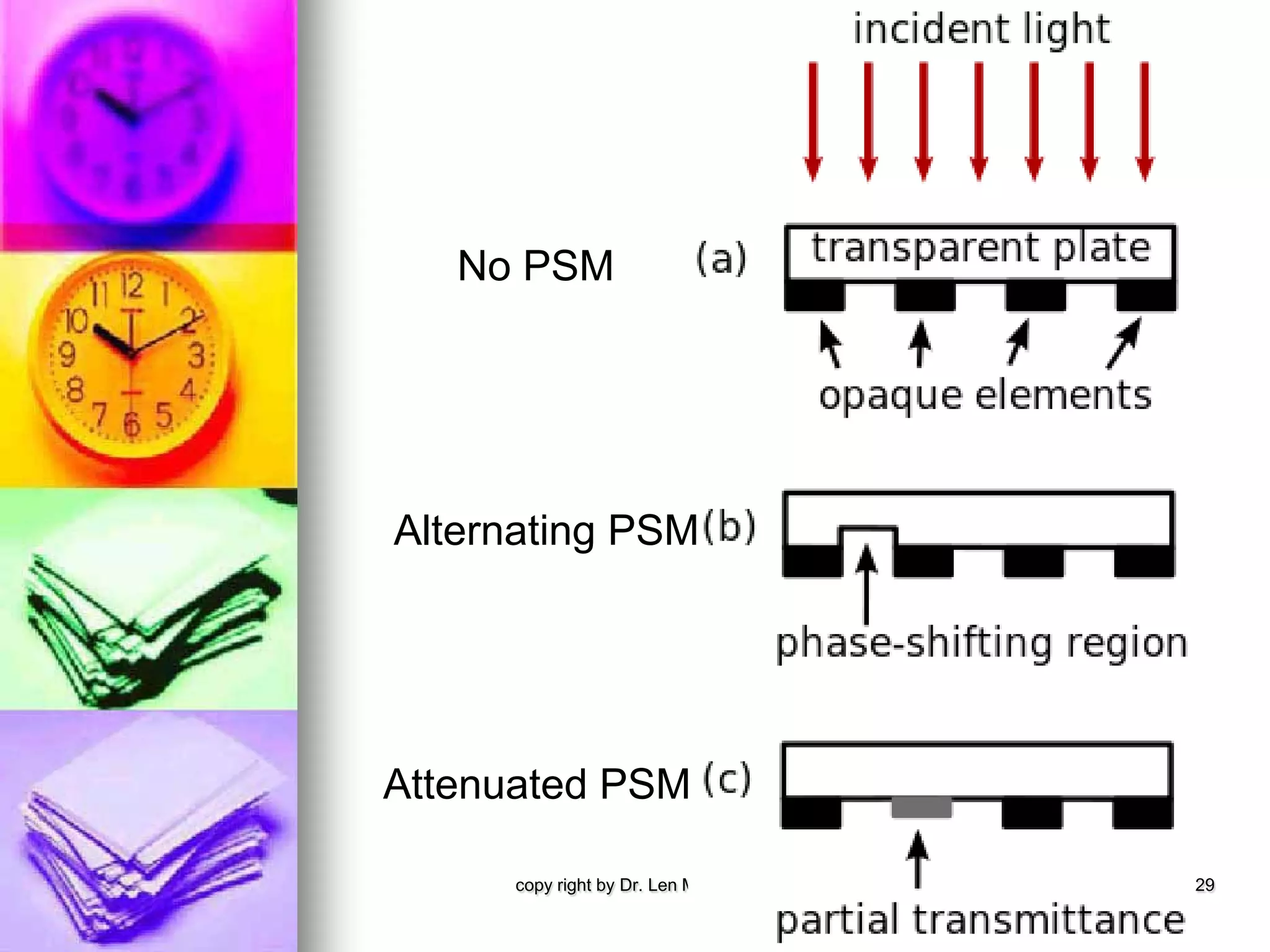
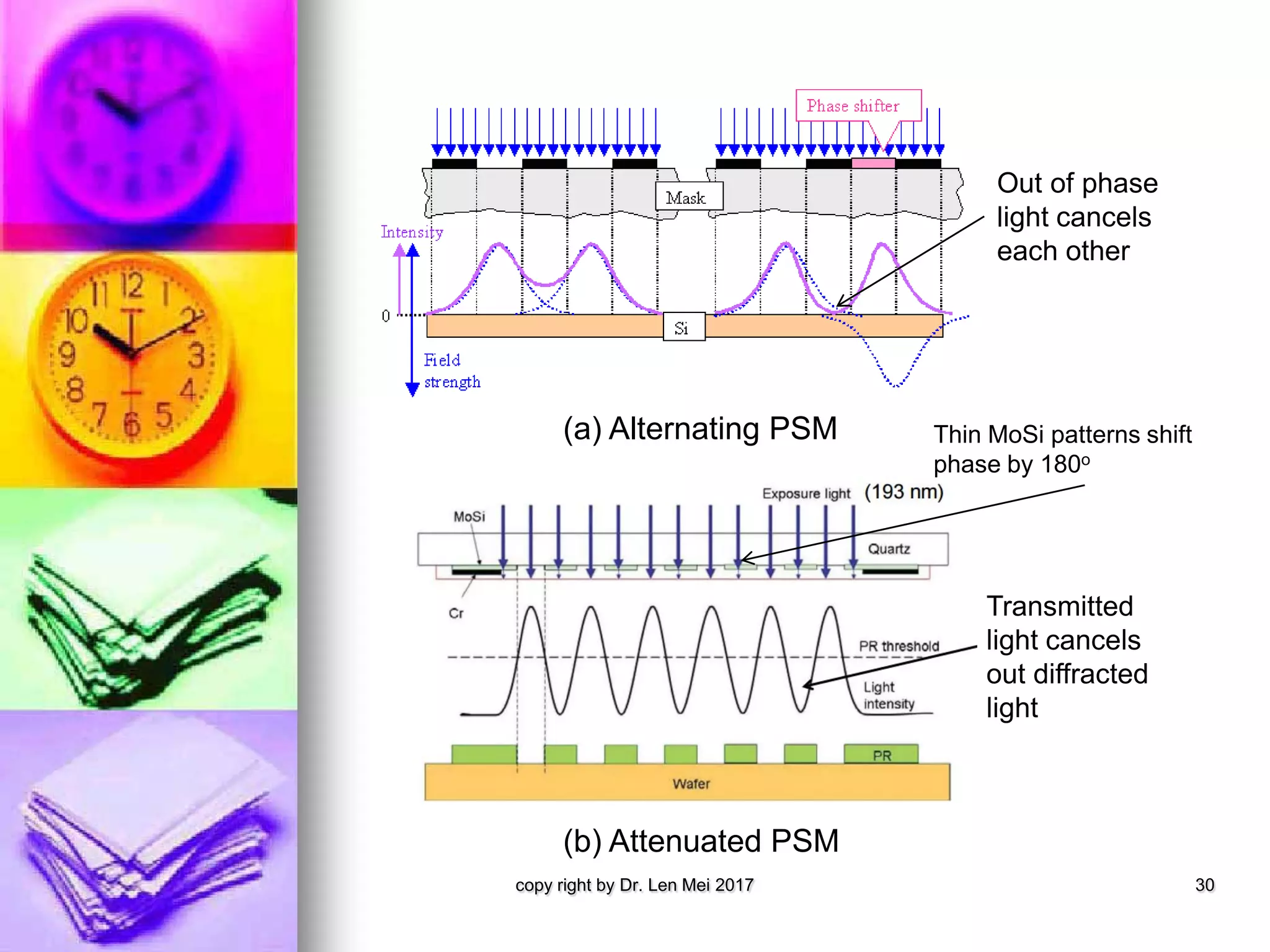
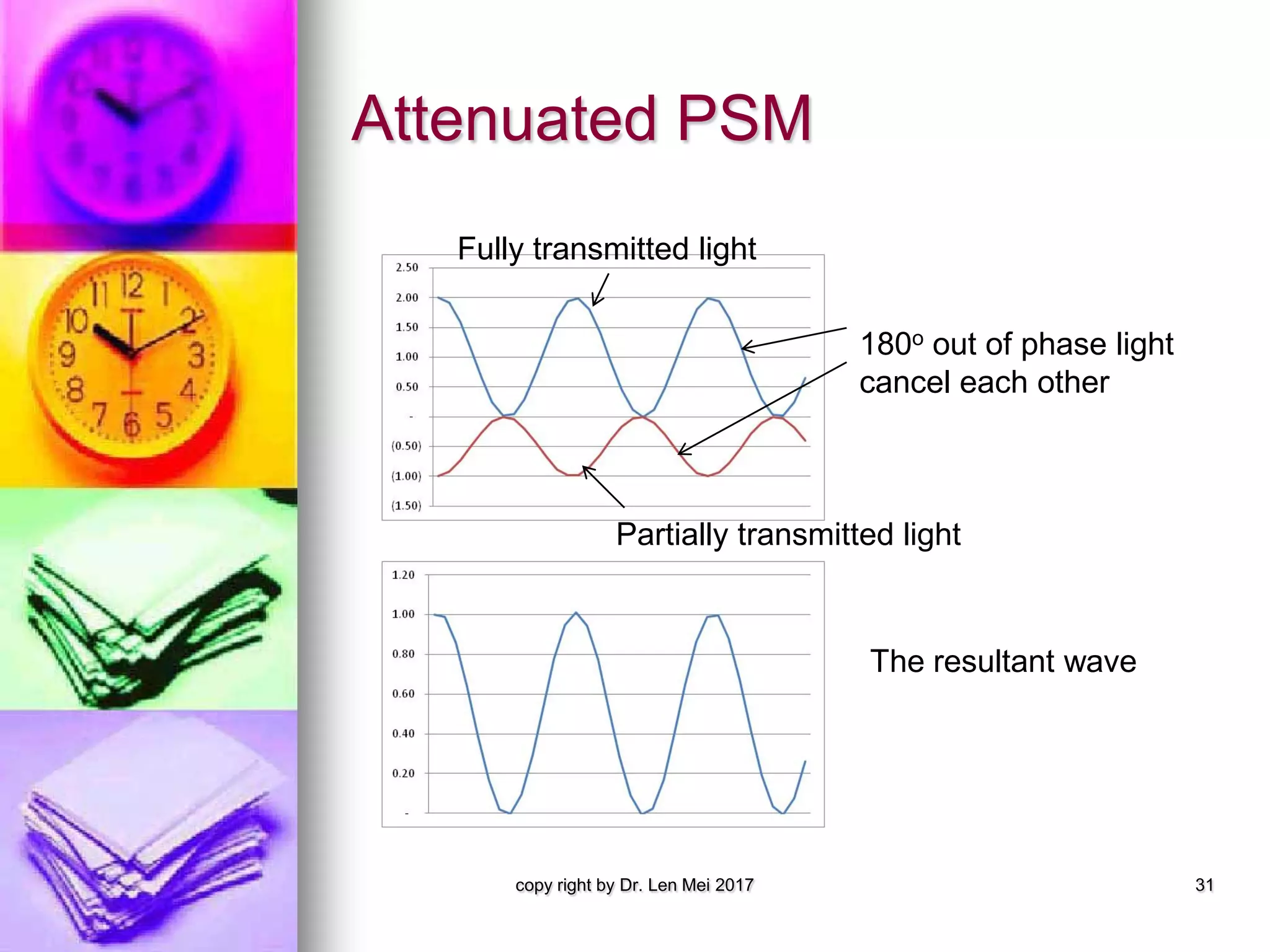
PSM improves resolution using phase differences; techniques include alternating and attenuated masks.
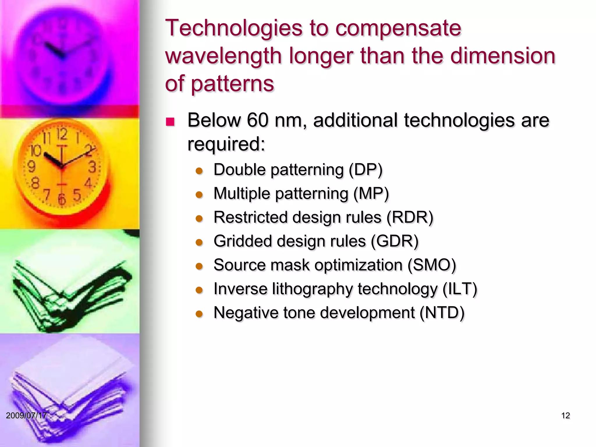
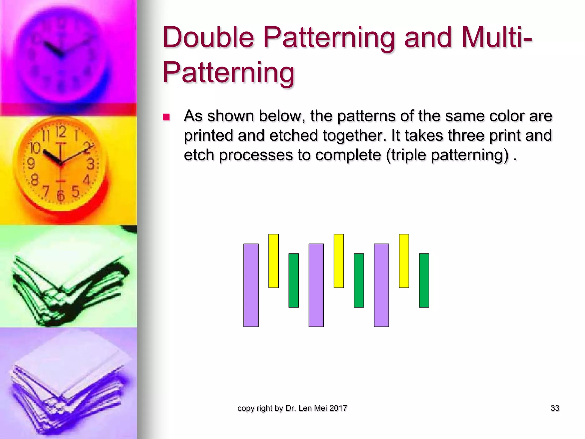
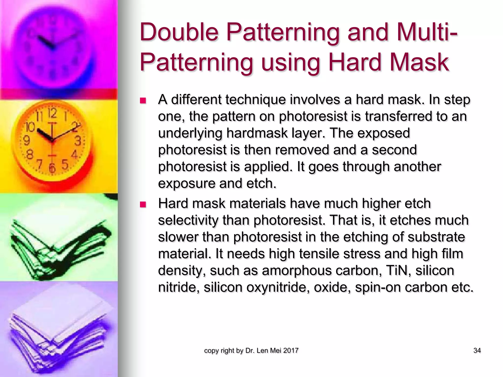
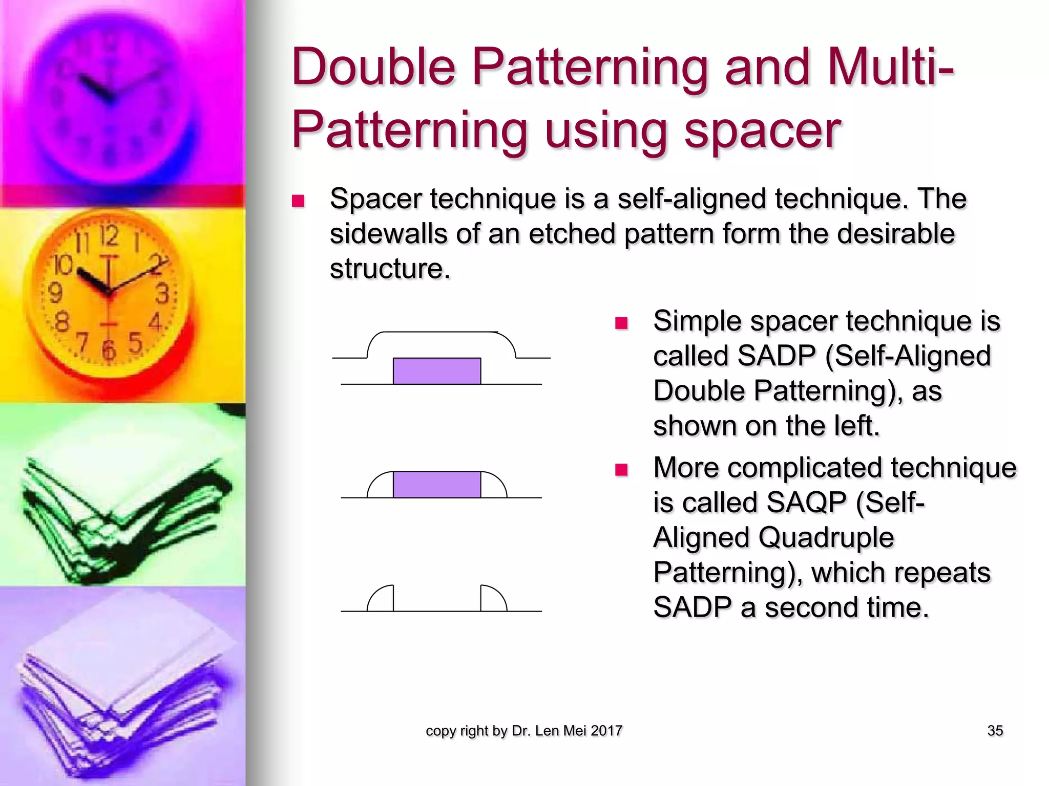
Double Patterning (DP) and Multi-Patterning (MP) techniques improve resolutions through multiple exposures.Extensive design alterations needed for DP and MP; introduces factors like cost and complexity in manufacturing.
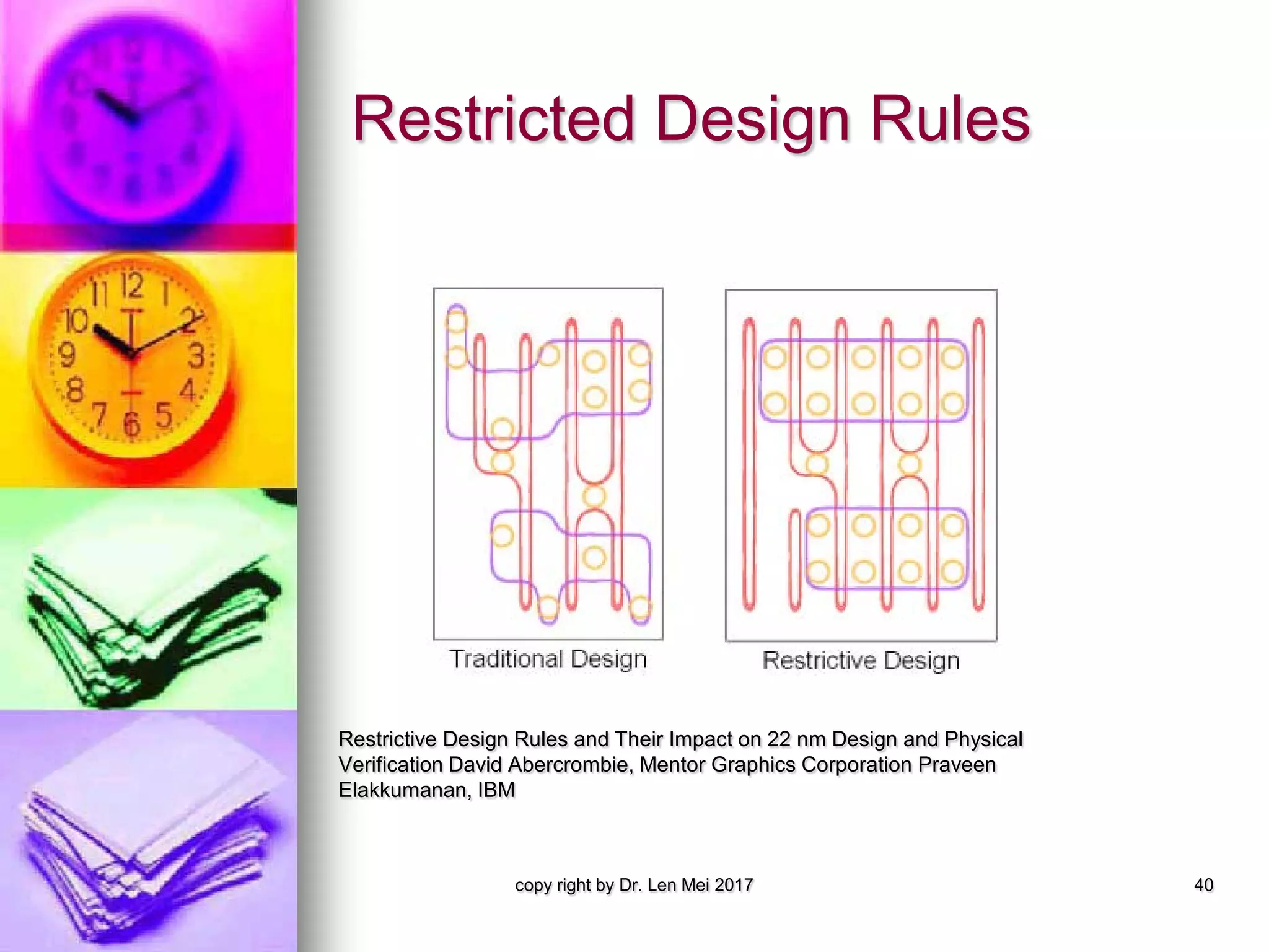
RDR and GDR establish new guidelines for design layouts to ease manufacturing complexities.
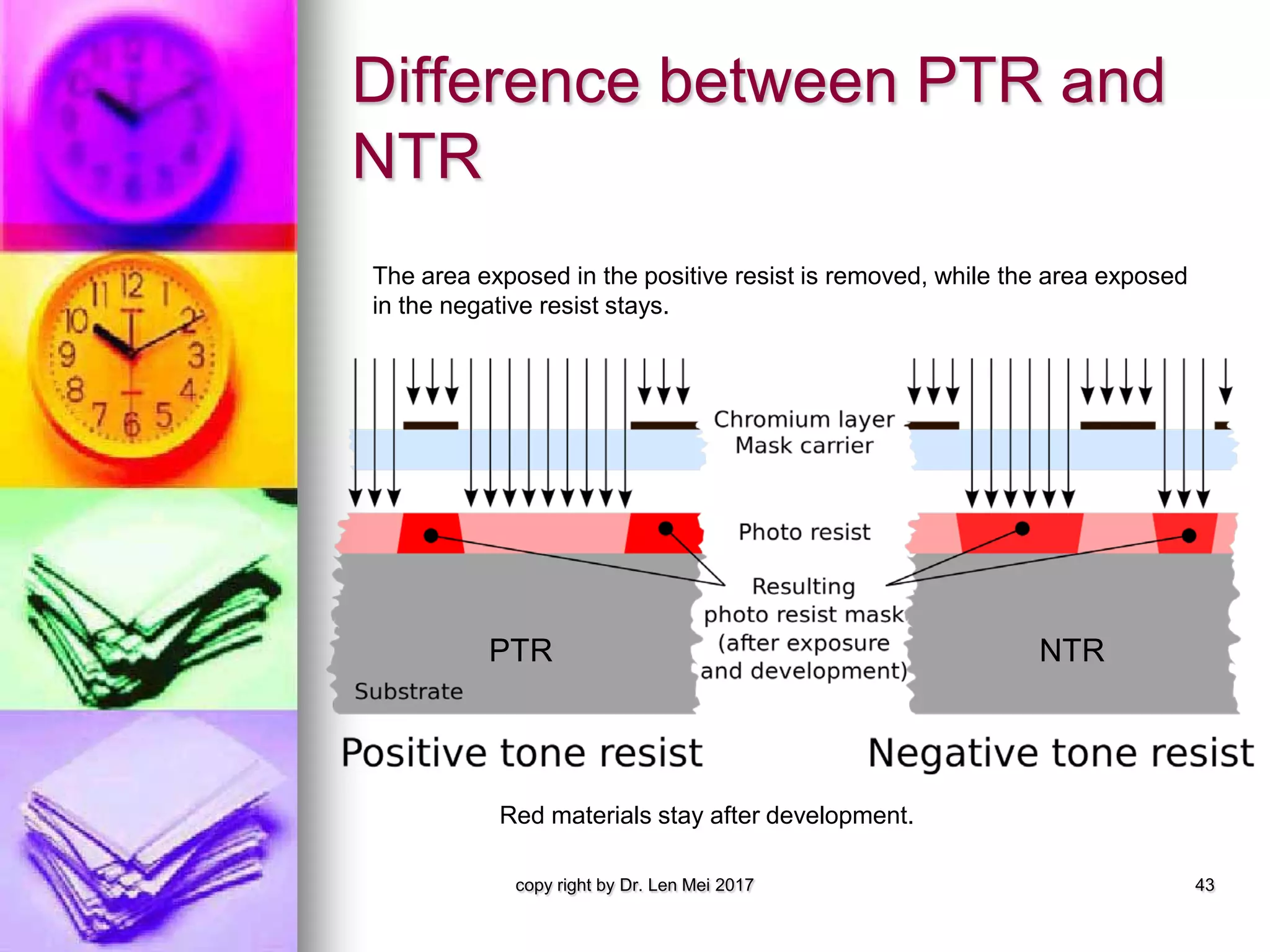
NTD uses negative tone resist to enhance lithographic process; advantages in line edge roughness and pattern resolution.
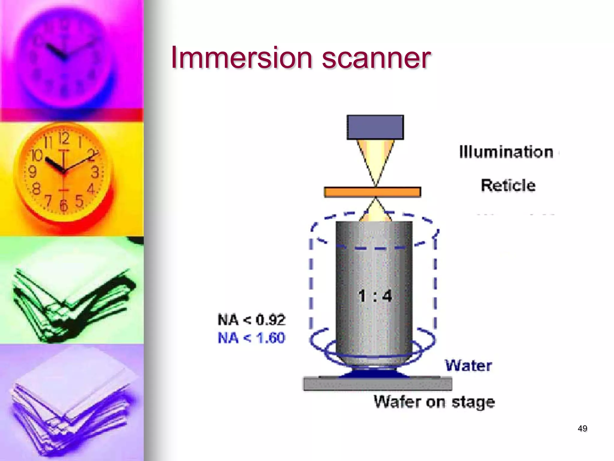
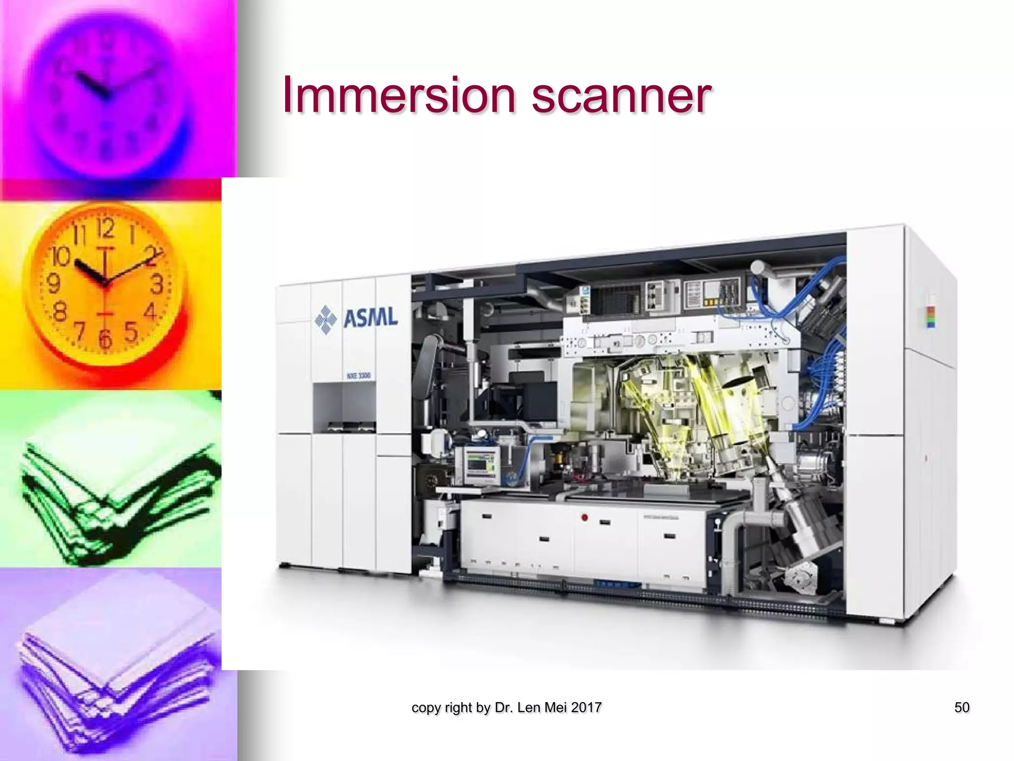
Advancements in photolithography tools focus on improved resolution through shorter wavelengths and enhanced systems.
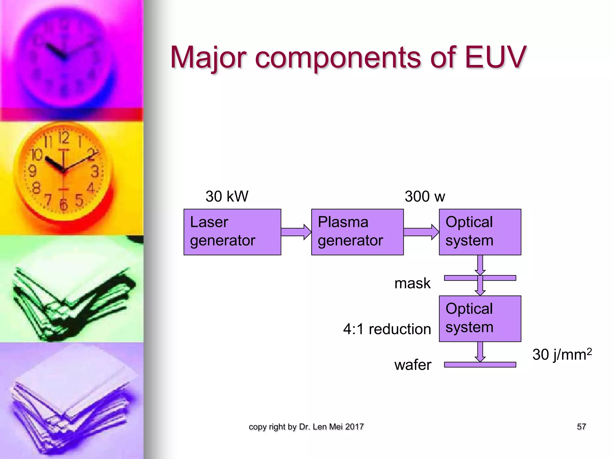
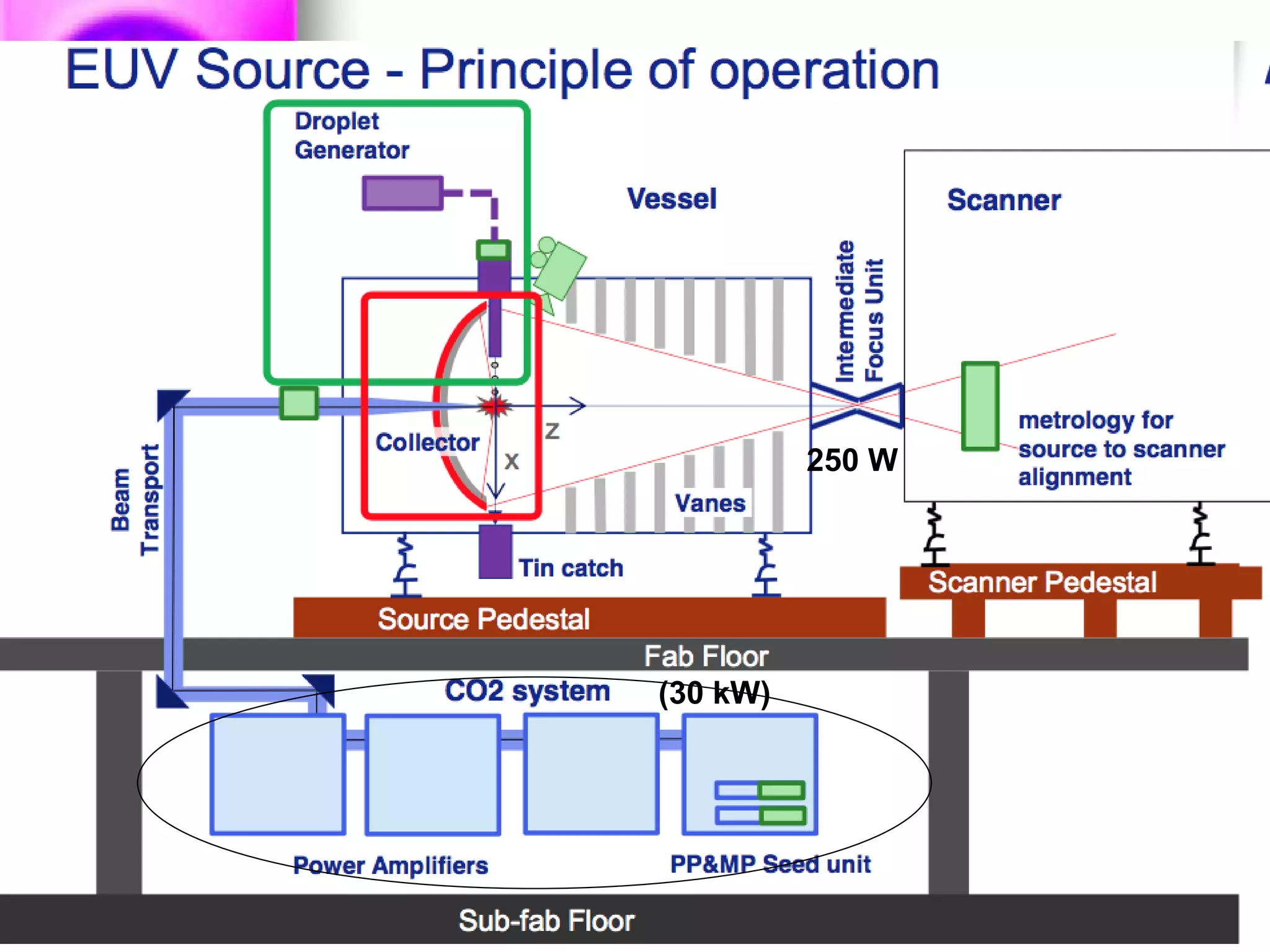
EUV represents the latest technology, facing challenges in cost, efficiency, and source power limitations.
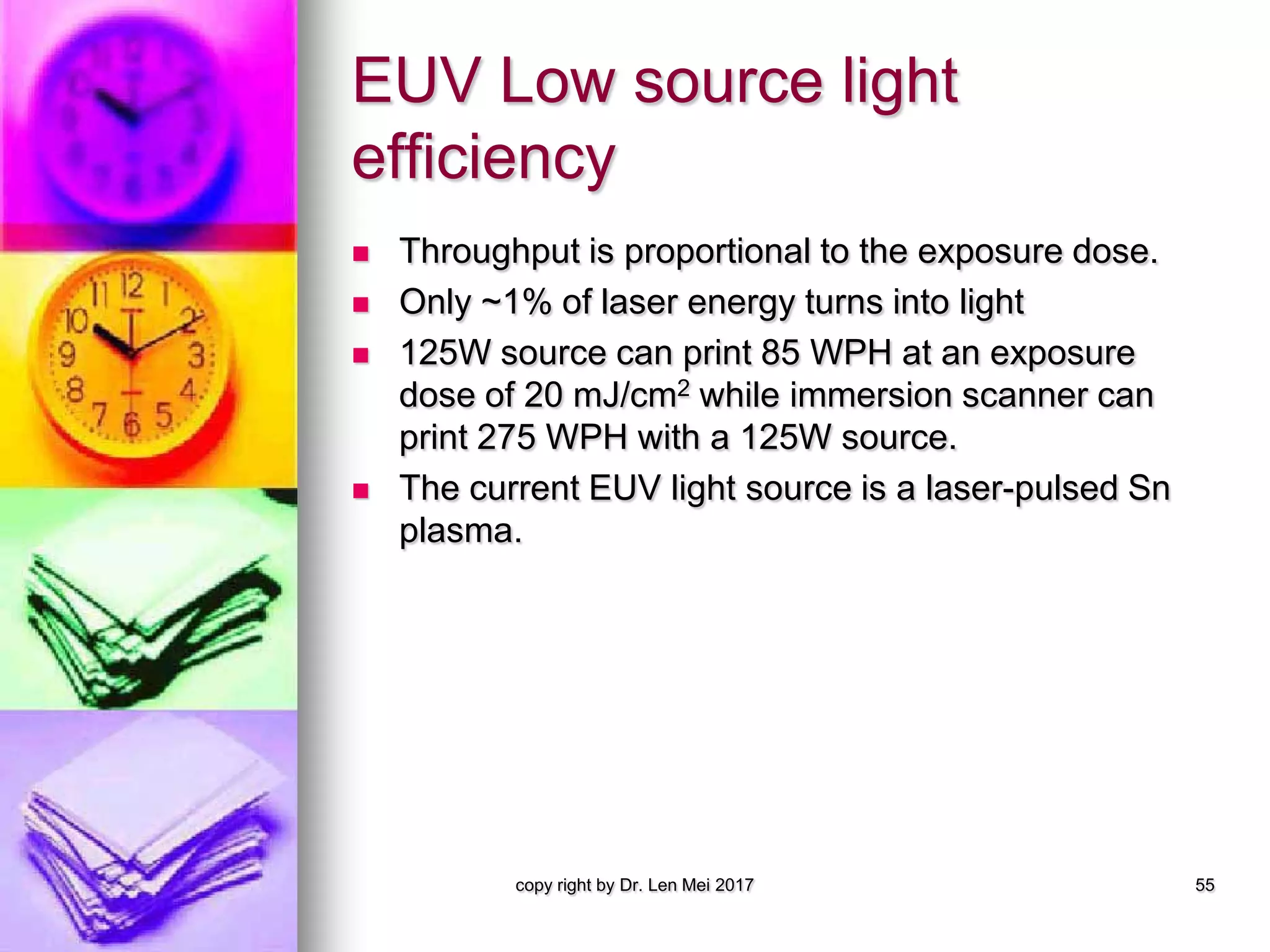
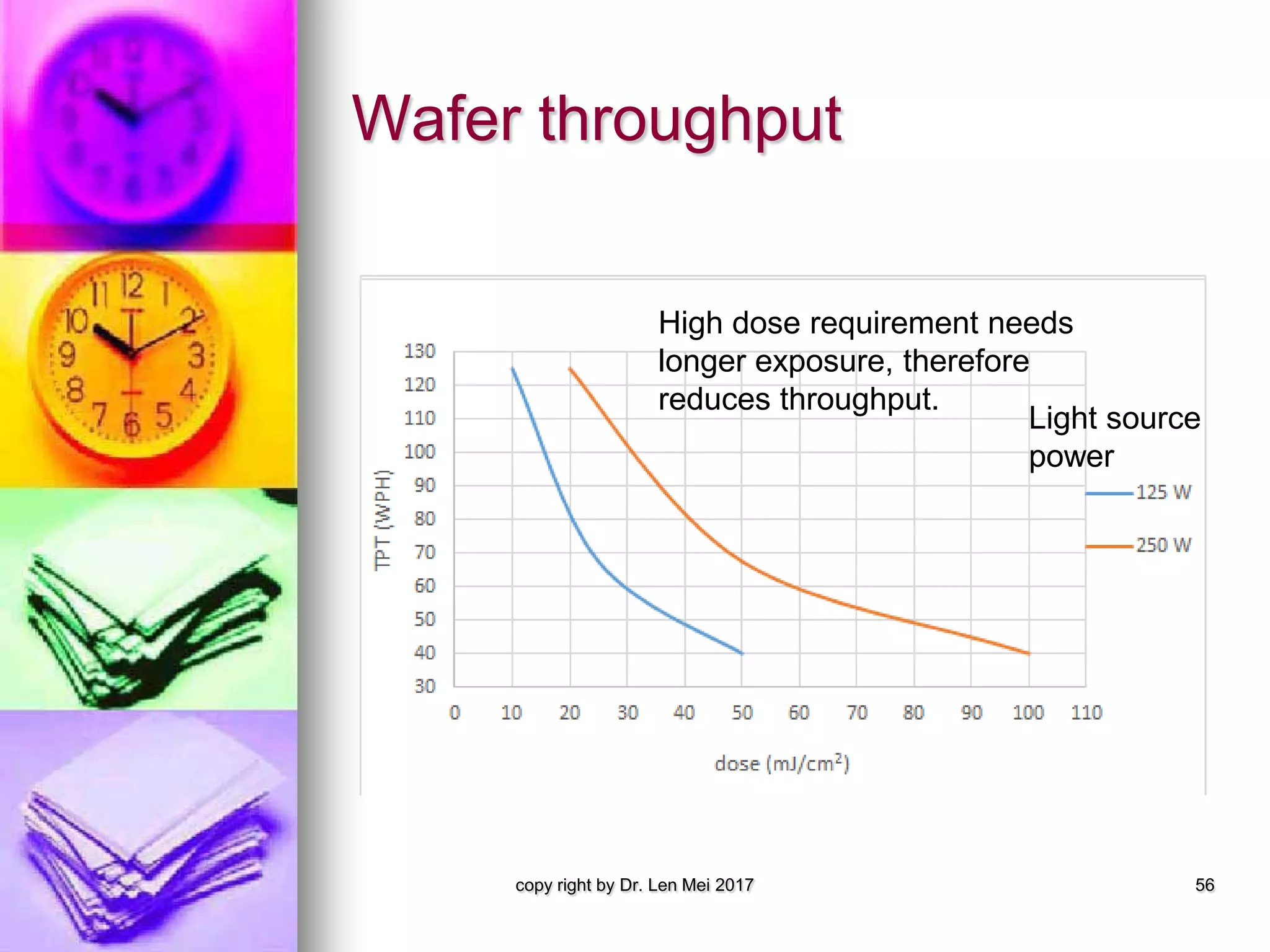
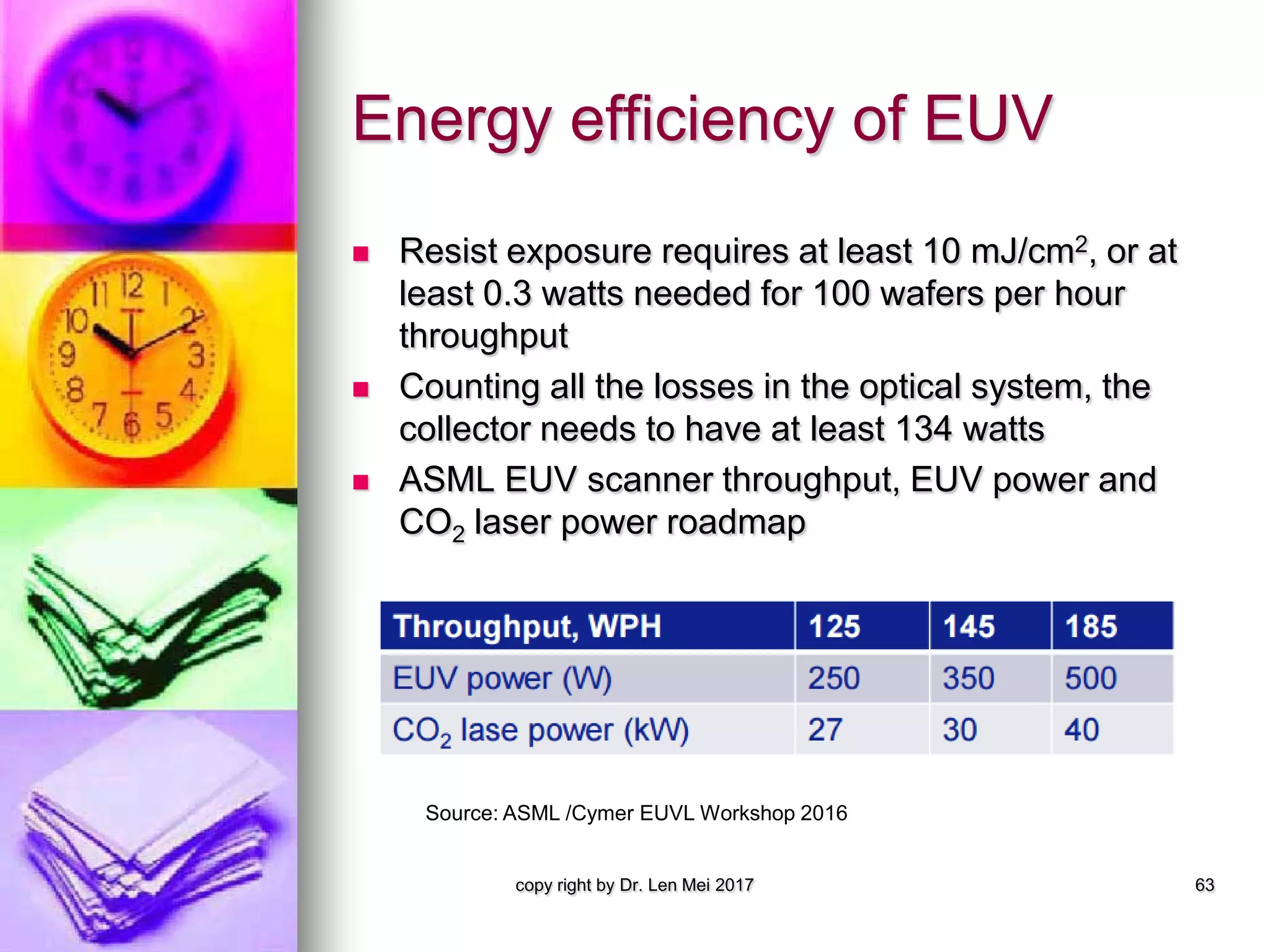
Efficiency of EUV scanning varies based on exposure energy and source limitations affecting throughput.
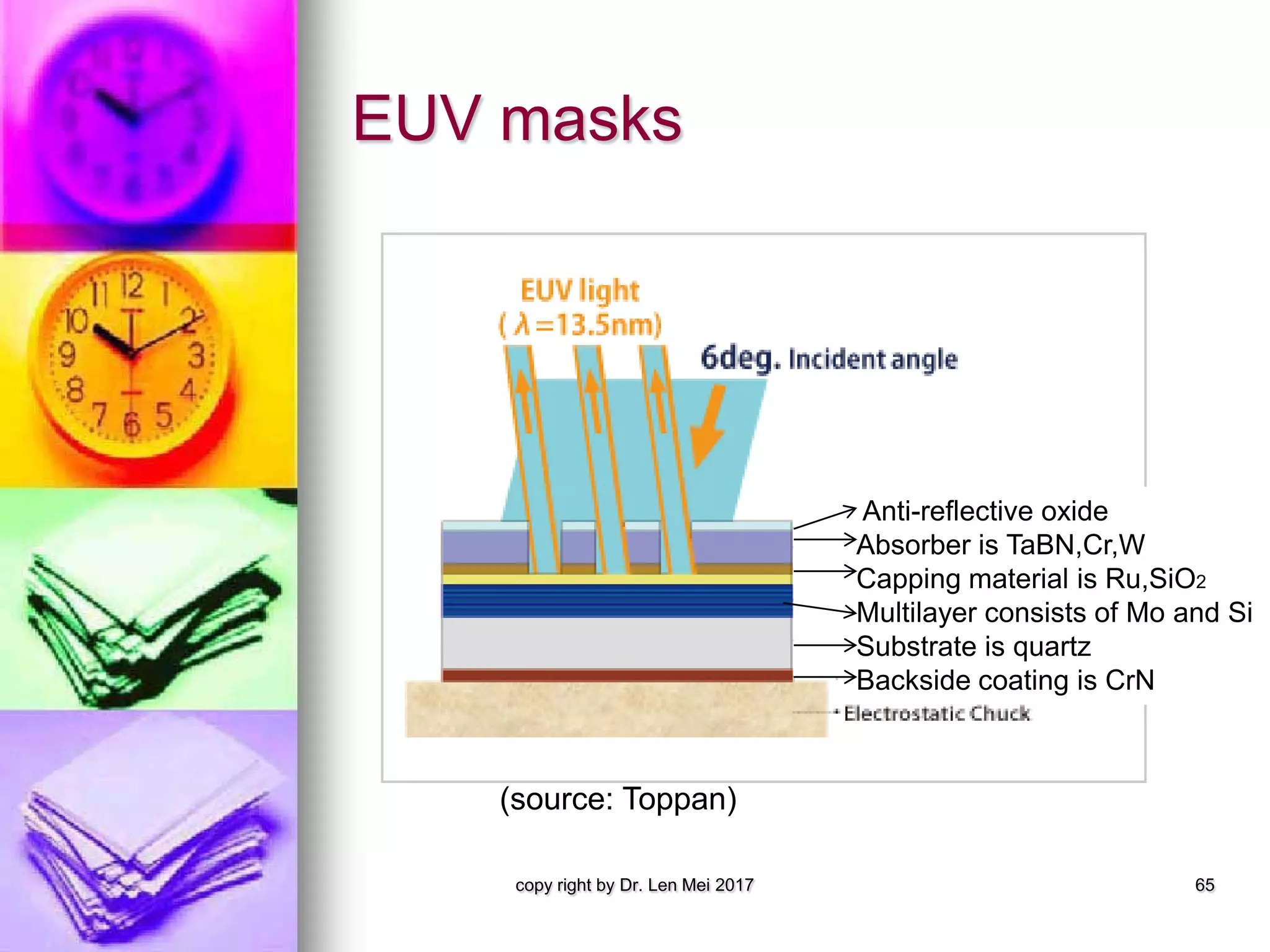
EUV mask designs must address thermal issues, defects, and contamination challenges for effective photolithography.
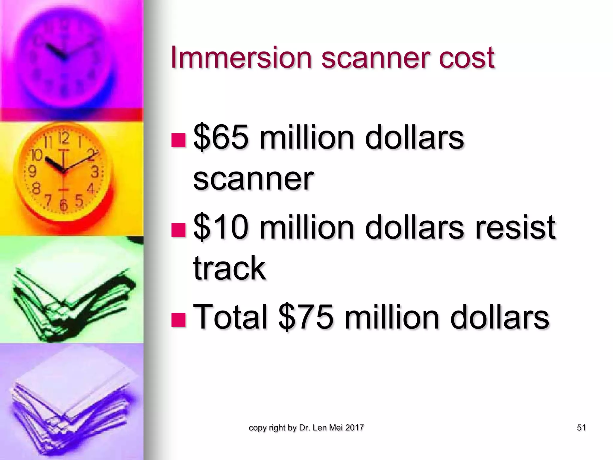
EUV scanner ownership entails significant costs, but offers necessary advances in semiconductor manufacturing.
Despite challenges, companies like Intel and TSMC plan to implement EUV to push technology nodes forward.


