Download to read offline
![Ishita Banerjeeet al Int. Journal of Engineering Research and Application
ISSN : 2248-9622, Vol. 3, Issue 6, Nov-Dec 2013, pp.75-78
RESEARCH ARTICLE
www.ijera.com
OPEN ACCESS
High Speed, Low Power, Area Efficient Mux-Add and Bec Based
Implementation of Carry Select Adder.
Ishita Banerjee
Assistant Professor New Horizon College of Engineering
Abstract
Adder being the basic hardware block of any arithmetic operation, the major constraint in the field of signal
processors, data processors to perform any operations are highly dependent on the adder performance of the
circuit. The gate level implementation of the carry select adder (CSLA) and modified carry select adder has
significantly reduced the area and power consumption which replaced the ripple carry adder (RCA) used in
modified CSLA with MUX-ADD block has further reduced the power consumption by efficiently utilizing the
area with faster performance.
I.
Introduction
Switching
speed
with
low
power
consumption is the major area needed to be
concentrated in modern trends of signal processing,
data processing and VLSI applications. To perform
any kind of signal and data processing operation, fast
arithmetic functions are to be calculated with higher
speed but non-degrading functionality. With the
advancements in the technology the factors to be taken
care during the hardware designs are frequency or
speed of operation, power consumption, area
utilization, circuit complexity, portability, robustness
etc. Thus while designing a modern high performance
processing element the optimization or best utilization
of the above mention factors are to be considered.
In any modern processing element the digital
adder block is a basic block which ensures the highspeed performance to a large extend. The drawback of
a simple ripple carry adder (RCA) is associated with
its propagation of carry bit which is highly overcome
by the implementation of high-speed, area efficient
carry select adder (CSLA)[1]. The traditional CSLA
independently generates multiple carry and then with
the selected carry generates the sum which reduces the
carry propagation delay of the RCA. The CSLA has
been modified further by reducing the area and power
consumption [2] to [4]. The implementation of squareroot CSLA (SQRT CSLA) [5] & [6] is modified with
the usage of binary to excess-1 converter (BEC)
instead of RCA [7] which claims an improved
performance.
In this paper the usage of an element ripple
carry adder is eliminated and instead a MUX-ADD
based arithmetic adder block is used which proves to
be logically stronger with a reduced propagation delay
in comparison to the other existing logic styles for
full-adders such as standard CMOS, complementary
pass transistor logic (CPL), double pass transistor
logic (DPL), swing restored CPL (SR-CPL) [8]. The
brief structure of MUX-ADD block is
www.ijera.com
discussed in section.2 . The BEC block structure is
also explained in section.3 . The delay and area is
evaluated for the used elemental blocks, modified
CSLA & MUX-ADD & BEC based CSLA in section.
4. The proposed designed is elaborated in section. 5.
The detailed simulation results in terms of delay,
power consumption and area along with the used
simulation and synthesis environment is discussed in
section. 6 .Finally the work concludes in section.7.
II.
MUX –ADD Block
The main idea of this paper is to replace RCA
from modified CSLA by a MUX-ADD unit for
improved performance. The MUX being a faster
hardware than direct adder block mainly improvises
the performance in terms of delay, area and power
consumption.The truth table of full adder is studied
and shown in table.1 with respect to carry input (Cin).
Cin
A
B
Sum
Carry
0
0
0
0
X
0
A
O
N
0
1
0
1
0
R
D
1
0
0
1
0
1
1
0
0
1
0
0
1
1
X
0
O
N
R
0
1
1
0
1
O
1
0
1
0
1
R
1
1
1
1
1
Table.1: Truth table of FA with respect to Cin
The MUX-ADD concept follows the following
algorithm:
begin
If Cin==’0’
Then
Sum=A xor B;
Carry=A and B;
Else if Cin==’1’
Then
Sum= A xnor B;
Carry=A or B;
75 | P a g e](https://image.slidesharecdn.com/m367578-131122003442-phpapp01/85/M367578-1-320.jpg)
![Ishita Banerjeeet al Int. Journal of Engineering Research and Application
ISSN : 2248-9622, Vol. 3, Issue 6, Nov-Dec 2013, pp.75-78
RESEARCH ARTICLE
www.ijera.com
OPEN ACCESS
High Speed, Low Power, Area Efficient Mux-Add and Bec Based
Implementation of Carry Select Adder.
Ishita Banerjee
Assistant Professor New Horizon College of Engineering
Abstract
Adder being the basic hardware block of any arithmetic operation, the major constraint in the field of signal
processors, data processors to perform any operations are highly dependent on the adder performance of the
circuit. The gate level implementation of the carry select adder (CSLA) and modified carry select adder has
significantly reduced the area and power consumption which replaced the ripple carry adder (RCA) used in
modified CSLA with MUX-ADD block has further reduced the power consumption by efficiently utilizing the
area with faster performance.
I.
Introduction
Switching
speed
with
low
power
consumption is the major area needed to be
concentrated in modern trends of signal processing,
data processing and VLSI applications. To perform
any kind of signal and data processing operation, fast
arithmetic functions are to be calculated with higher
speed but non-degrading functionality. With the
advancements in the technology the factors to be taken
care during the hardware designs are frequency or
speed of operation, power consumption, area
utilization, circuit complexity, portability, robustness
etc. Thus while designing a modern high performance
processing element the optimization or best utilization
of the above mention factors are to be considered.
In any modern processing element the digital
adder block is a basic block which ensures the highspeed performance to a large extend. The drawback of
a simple ripple carry adder (RCA) is associated with
its propagation of carry bit which is highly overcome
by the implementation of high-speed, area efficient
carry select adder (CSLA)[1]. The traditional CSLA
independently generates multiple carry and then with
the selected carry generates the sum which reduces the
carry propagation delay of the RCA. The CSLA has
been modified further by reducing the area and power
consumption [2] to [4]. The implementation of squareroot CSLA (SQRT CSLA) [5] & [6] is modified with
the usage of binary to excess-1 converter (BEC)
instead of RCA [7] which claims an improved
performance.
In this paper the usage of an element ripple
carry adder is eliminated and instead a MUX-ADD
based arithmetic adder block is used which proves to
be logically stronger with a reduced propagation delay
in comparison to the other existing logic styles for
full-adders such as standard CMOS, complementary
pass transistor logic (CPL), double pass transistor
logic (DPL), swing restored CPL (SR-CPL) [8]. The
brief structure of MUX-ADD block is
www.ijera.com
discussed in section.2 . The BEC block structure is
also explained in section.3 . The delay and area is
evaluated for the used elemental blocks, modified
CSLA & MUX-ADD & BEC based CSLA in section.
4. The proposed designed is elaborated in section. 5.
The detailed simulation results in terms of delay,
power consumption and area along with the used
simulation and synthesis environment is discussed in
section. 6 .Finally the work concludes in section.7.
II.
MUX –ADD Block
The main idea of this paper is to replace RCA
from modified CSLA by a MUX-ADD unit for
improved performance. The MUX being a faster
hardware than direct adder block mainly improvises
the performance in terms of delay, area and power
consumption.The truth table of full adder is studied
and shown in table.1 with respect to carry input (Cin).
Cin
A
B
Sum
Carry
0
0
0
0
X
0
A
O
N
0
1
0
1
0
R
D
1
0
0
1
0
1
1
0
0
1
0
0
1
1
X
0
O
N
R
0
1
1
0
1
O
1
0
1
0
1
R
1
1
1
1
1
Table.1: Truth table of FA with respect to Cin
The MUX-ADD concept follows the following
algorithm:
begin
If Cin==’0’
Then
Sum=A xor B;
Carry=A and B;
Else if Cin==’1’
Then
Sum= A xnor B;
Carry=A or B;
75 | P a g e](https://image.slidesharecdn.com/m367578-131122003442-phpapp01/75/M367578-1-2048.jpg)
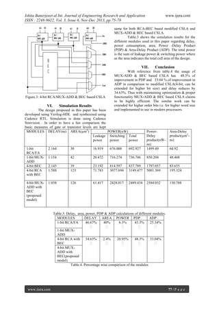
![Ishita Banerjeeet al Int. Journal of Engineering Research and Application
ISSN : 2248-9622, Vol. 3, Issue 6, Nov-Dec 2013, pp.75-78
www.ijera.com
References
[1]
[2]
[3]
[4]
[5]
[6]
[7]
[8]
O. J. Bedrij, “Carry-select adder,” IRE
Trans. Electron. Comput., pp.340–344,
1962.
B. Ramkumar, H. M. Kittur, and P. M.
Kannan, “ASIC implementation of modified
faster carry save adder,”Eur. J. Sci. Res.,
vol. 42, no. 1, pp. 53–58, 2010.
T. Y. Ceiang and M. J. Hsiao, “Carry-select
adder
using
single
ripple
carry
adder,”Electron. Lett., vol. 34, no. 22, pp.
2101–2103, Oct. 1998.
Y. Kim and L.-S. Kim, “64-bit carry-select
adder with reduced area,” Electron. Lett.,
vol. 37, no. 10, pp. 614–615, May 2001.
J. M. Rabaey, Digtal Integrated Circuits—A
Design Perspective. Upper Saddle River,
NJ: Prentice-Hall, 2001.
Y. He, C. H. Chang, and J. Gu, “An area
efficient 64-bit square root carry-select
adder for low power applications,” inProc.
IEEE Int. Symp. Circuits Syst., 2005, vol. 4,
pp. 4082–4085.
B.ramkumar and Harish M Kittur, “Loe
power area efficient Carry select adder”,
IEEE transaction on VLSI Systems, Vol:20,
No.2,February 2012,pp. 371–375.
Mariano Aguirre Hernandez and Monico
Linares Aranda, “CMOS Full Adders for
Energy
efficient
arithmetic
application”,IEEE transactions on VLSI
Systems,Vol.19,No.4, April 2011,pp.718721.
www.ijera.com
78 | P a g e](https://image.slidesharecdn.com/m367578-131122003442-phpapp01/85/M367578-4-320.jpg)

This research article presents a high-speed, low power, and area-efficient implementation of the carry select adder (CSLA) utilizing a mux-add and binary to excess-1 converter (BEC). The proposed design improves upon traditional adder architectures by significantly reducing power consumption and propagation delay while optimizing area usage, making it suitable for modern processing applications. Simulation results demonstrate a 48.3% improvement in power-delay product and a 34.63% reduction in delay compared to modified CSLA, confirming the design's efficiency.