Downloaded 1,488 times

![REFERENCES
[1] B. Ramkumar, Harish M Kittur “Low power and Area efficient carry select adder,”IEEE
Trans,Vol.20,Feb 2012.
[2] T. Y. Ceiang and M. J. Hsiao, “Carry-select adder using single ripple carry adder,” Electron.
Lett., vol. 34, no. 22, pp. 2101–2103, Oct. 1998.
[3] Y. Kim and L.-S. Kim, “64-bit carry-select adder with reduced area,” Electron. Lett., vol.
37, no. 10, pp. 614–615, May 2001.
[4] J. M. Rabaey, Digtal Integrated Circuits—A Design Perspective.Upper Saddle River, NJ:
Prentice-Hall, 2001.
[5] Samir Palnitkar, “Verilog Hdl: A Guide to Digital Design and Synthesis”2005,2nd
Edition.](https://image.slidesharecdn.com/low-powerareaefficientcarryselectadder-140326094912-phpapp02/85/Low-power-area-efficient-carry-select-adder-21-320.jpg)


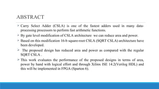
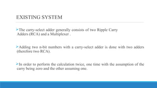
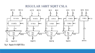
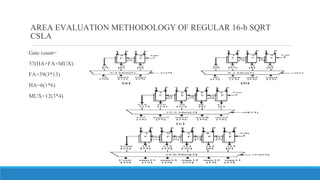
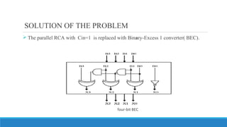
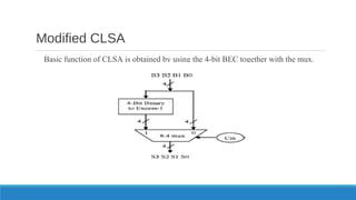
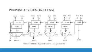
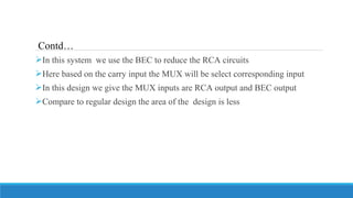
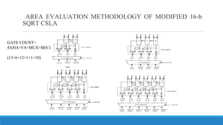
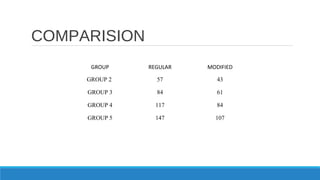
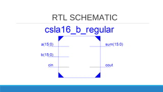
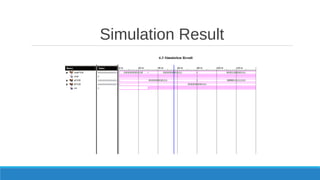
This document proposes a modified carry select adder design to reduce area and power consumption compared to a regular carry select adder. A carry select adder uses two ripple carry adders and a multiplexer to perform addition. The proposed design replaces one of the ripple carry adders with a binary-excess-1 converter to reduce the number of full adders. Simulation results show the modified design reduces area by reducing the gate count and also lowers power consumption compared to a regular carry select adder design. The modified design has applications in arithmetic logic units, high-speed multiplications, and advanced microprocessor designs due to its lower area and power.