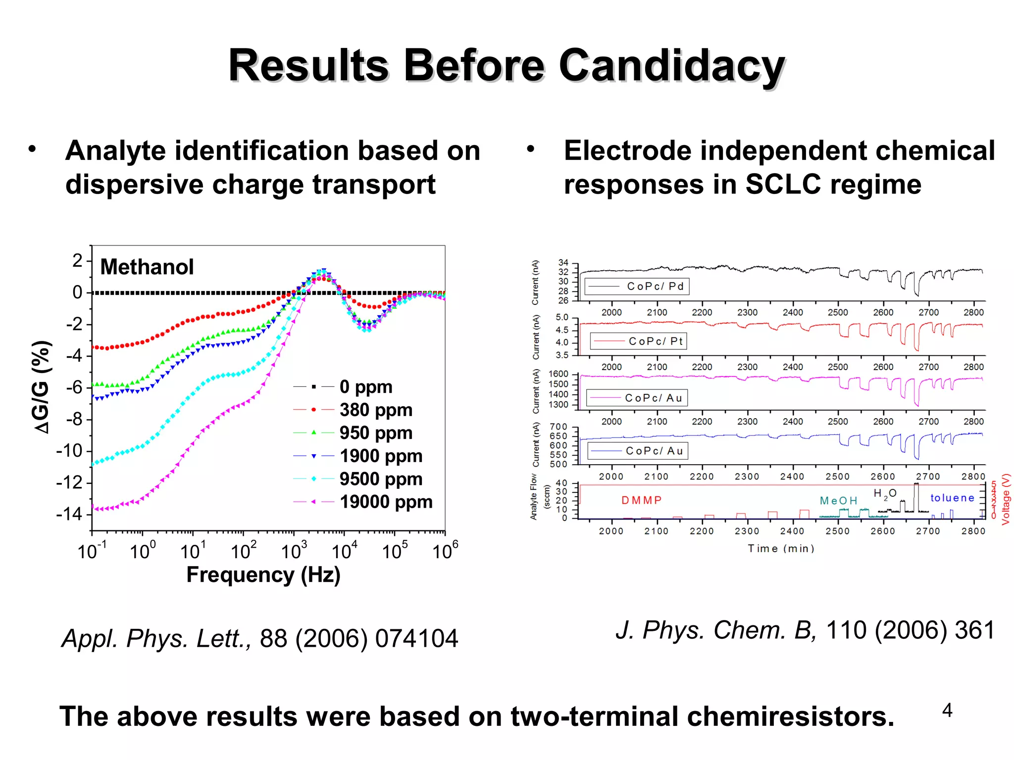
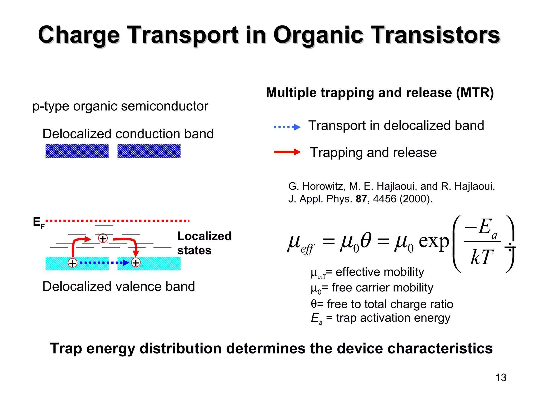
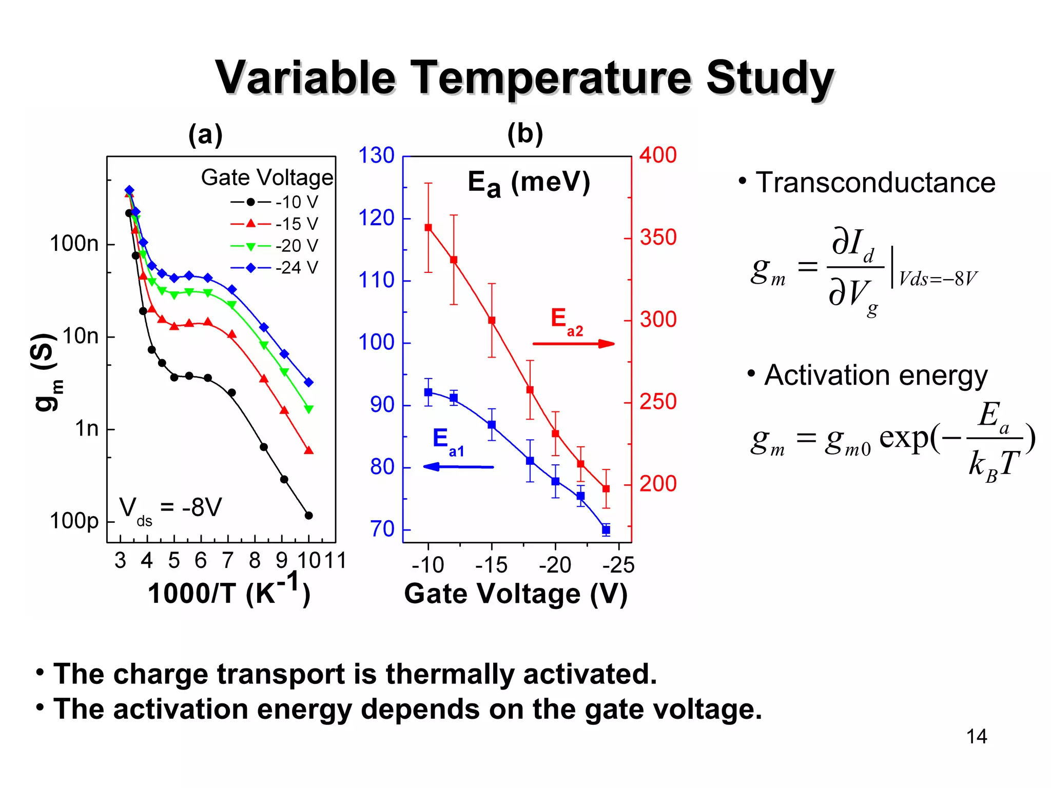
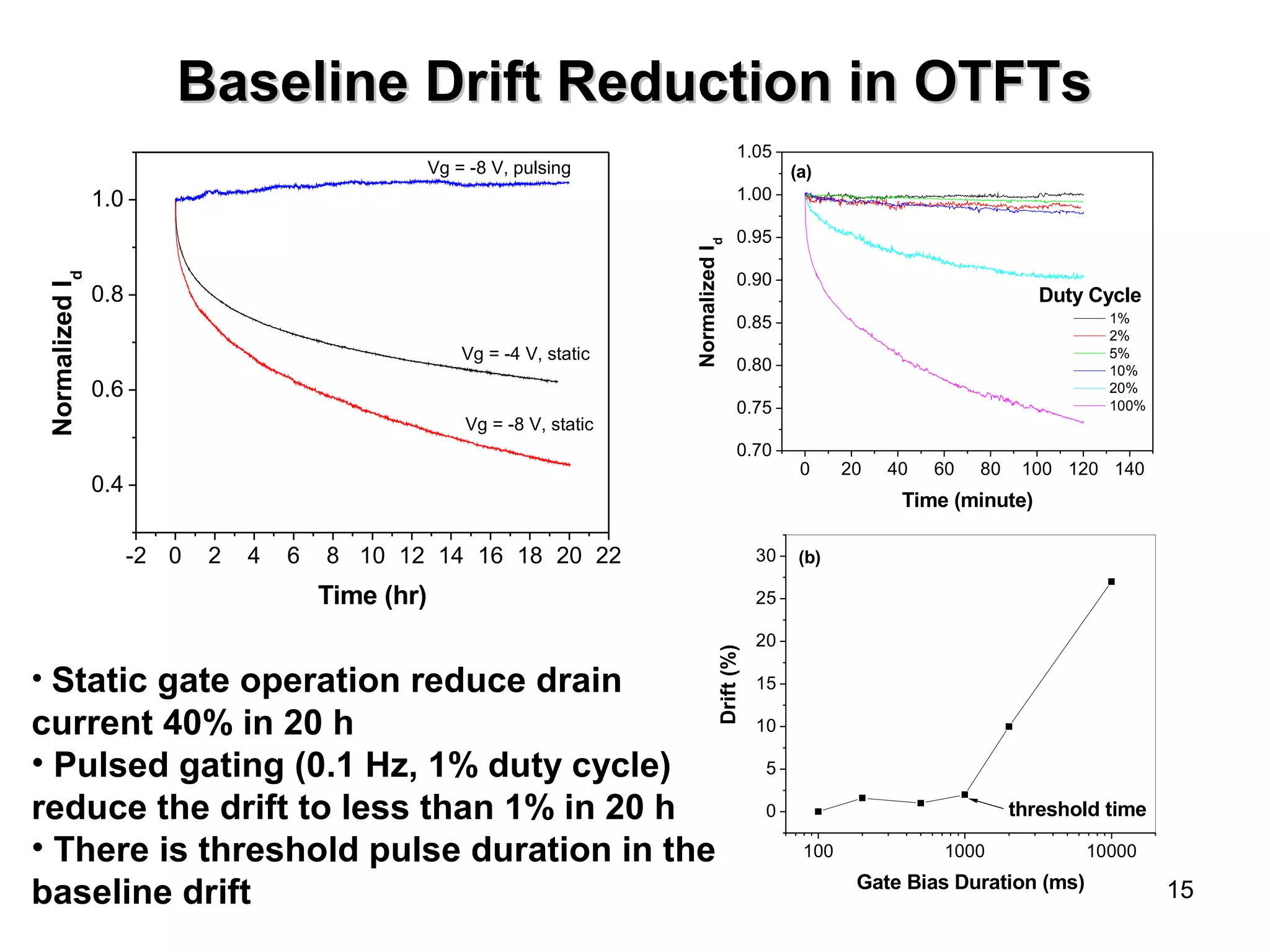
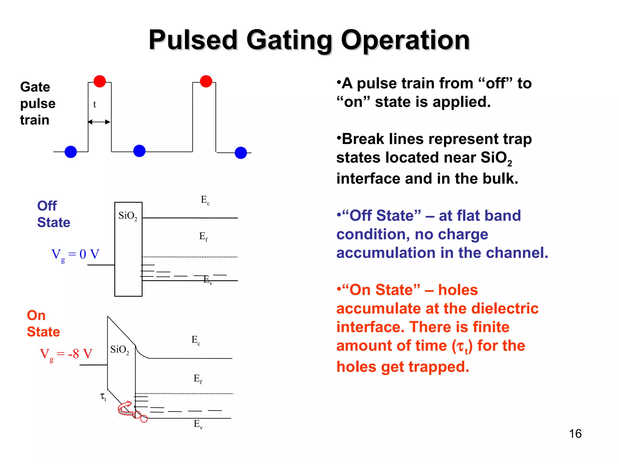
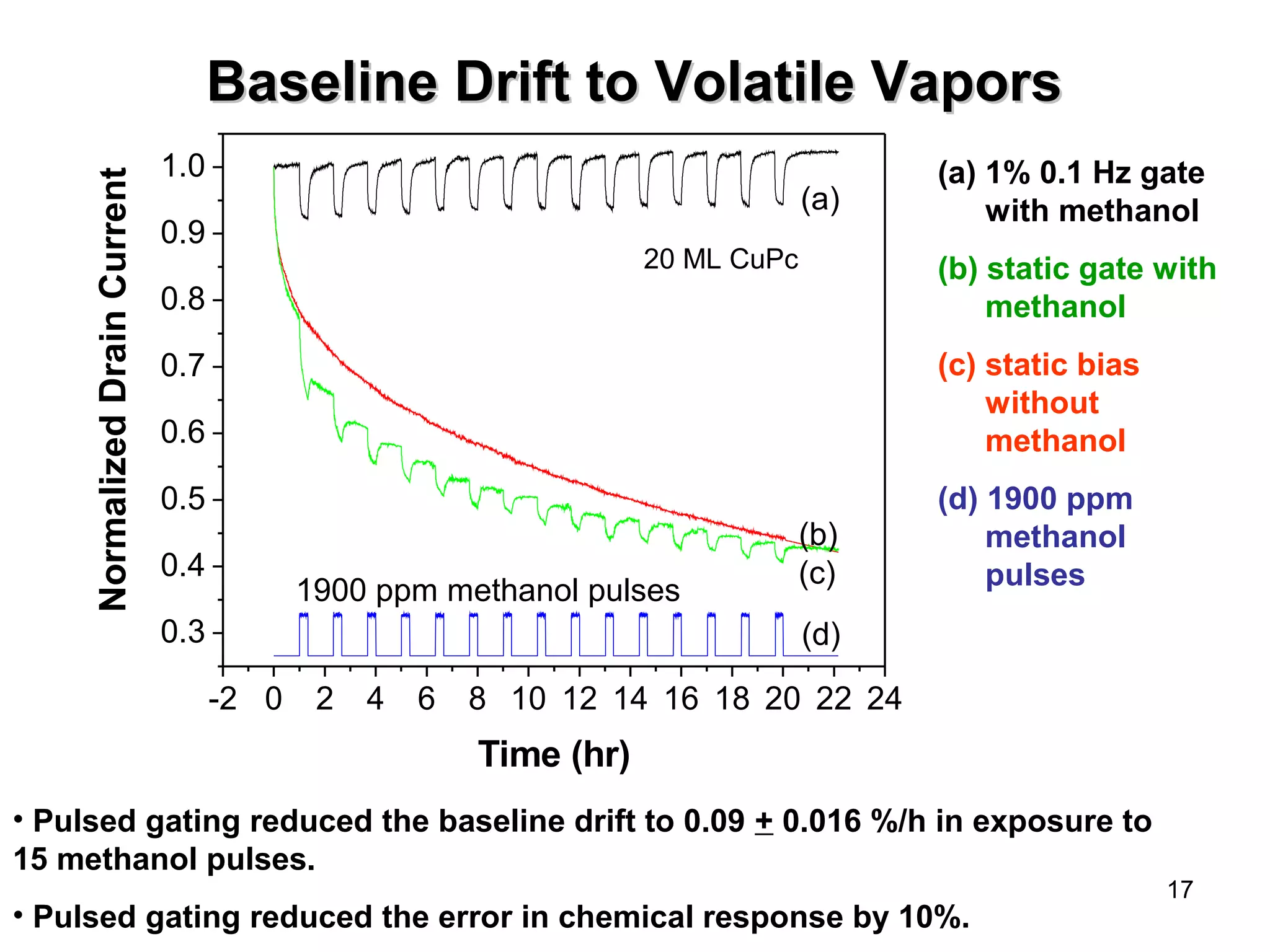
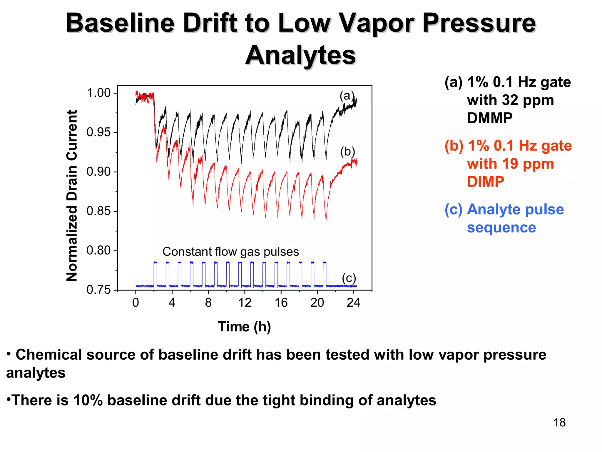
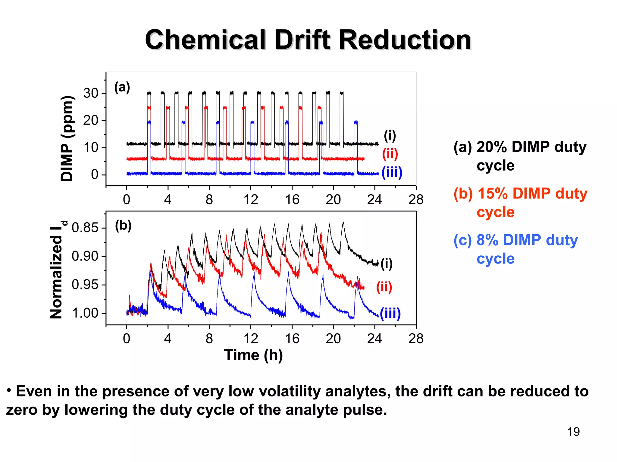
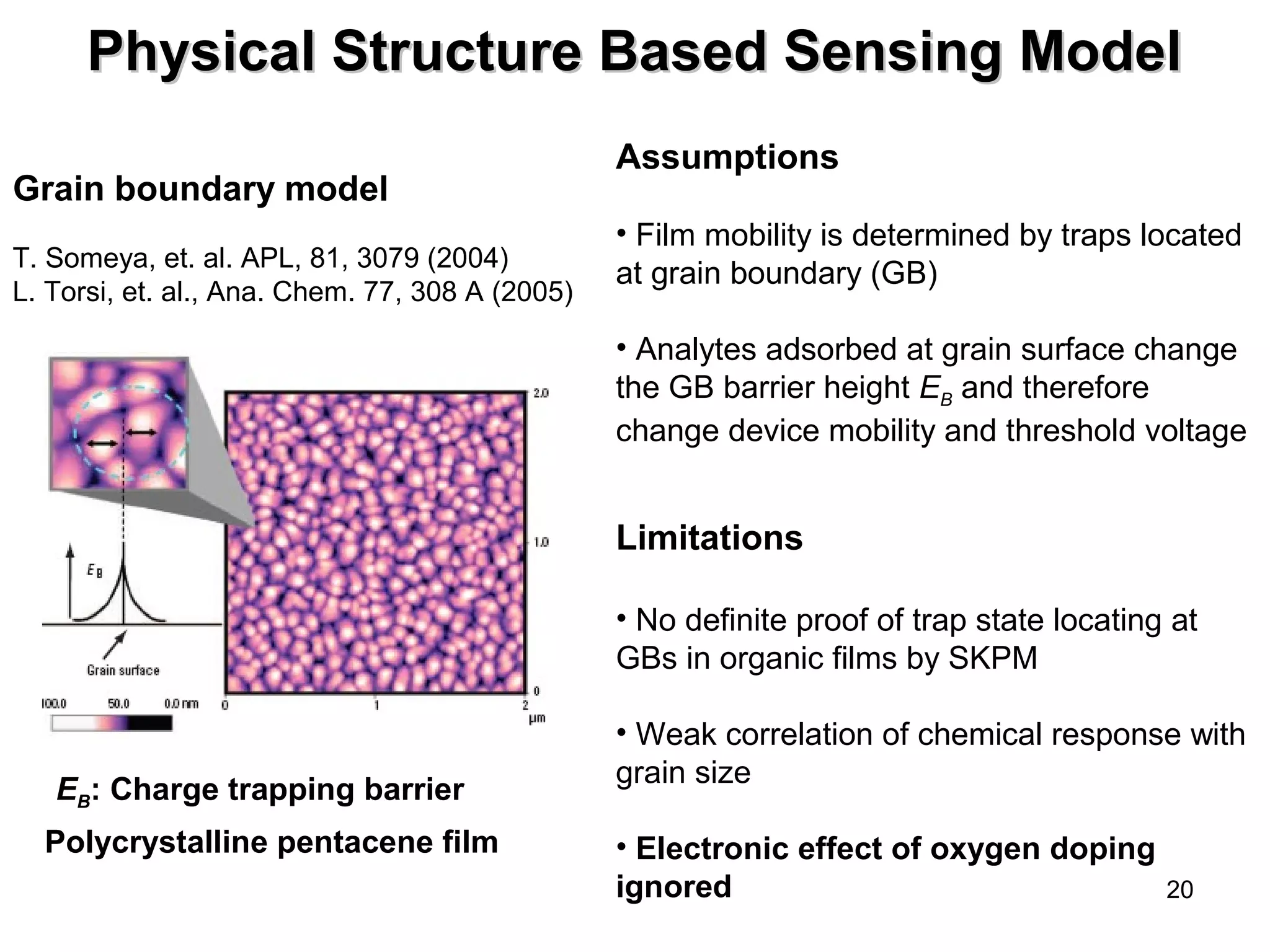
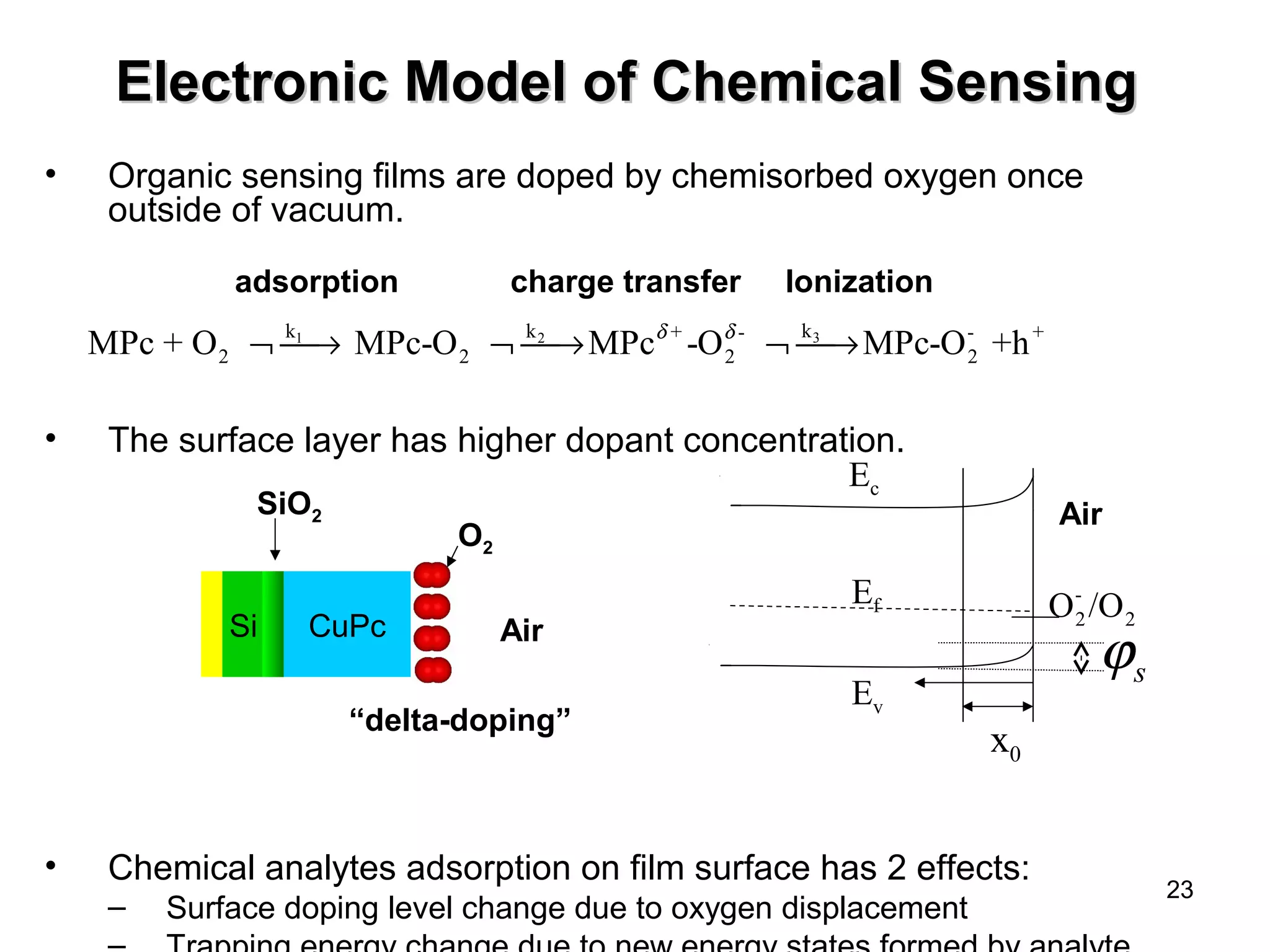
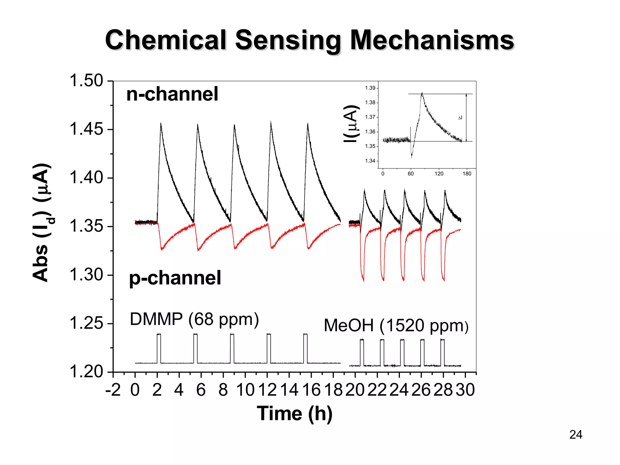
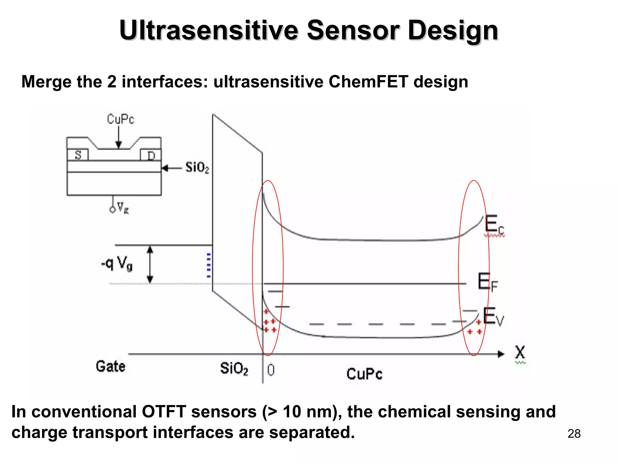
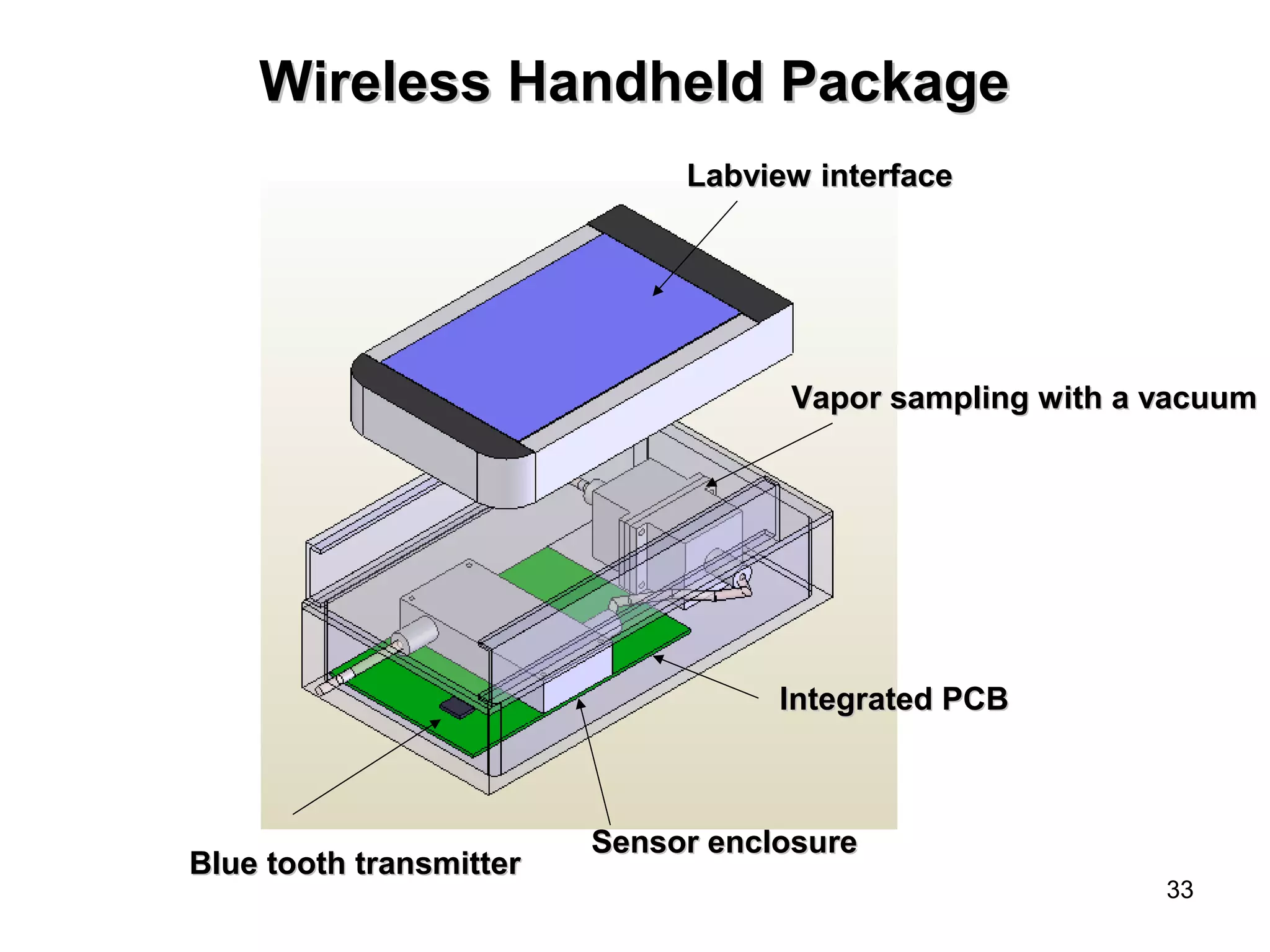
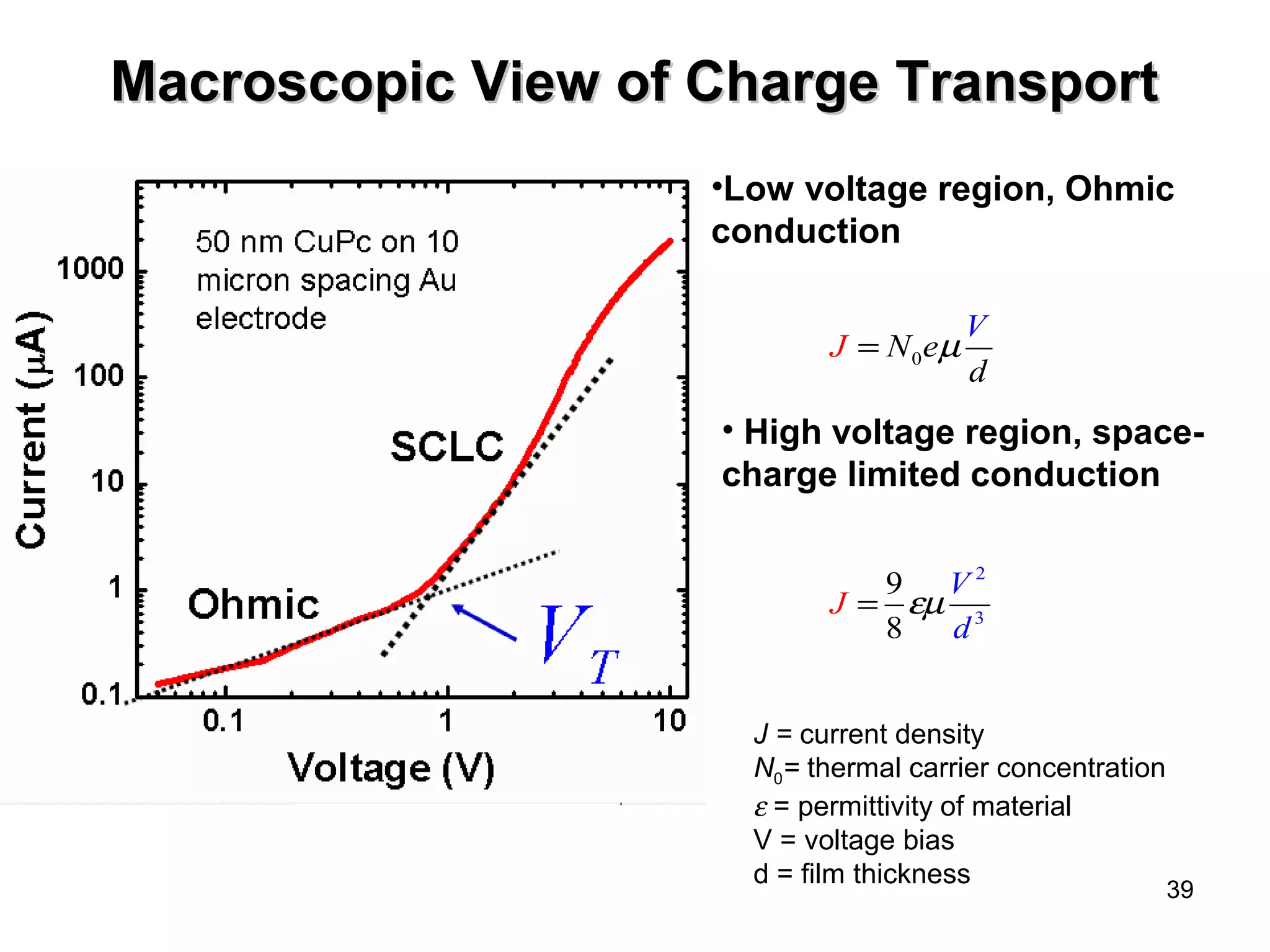
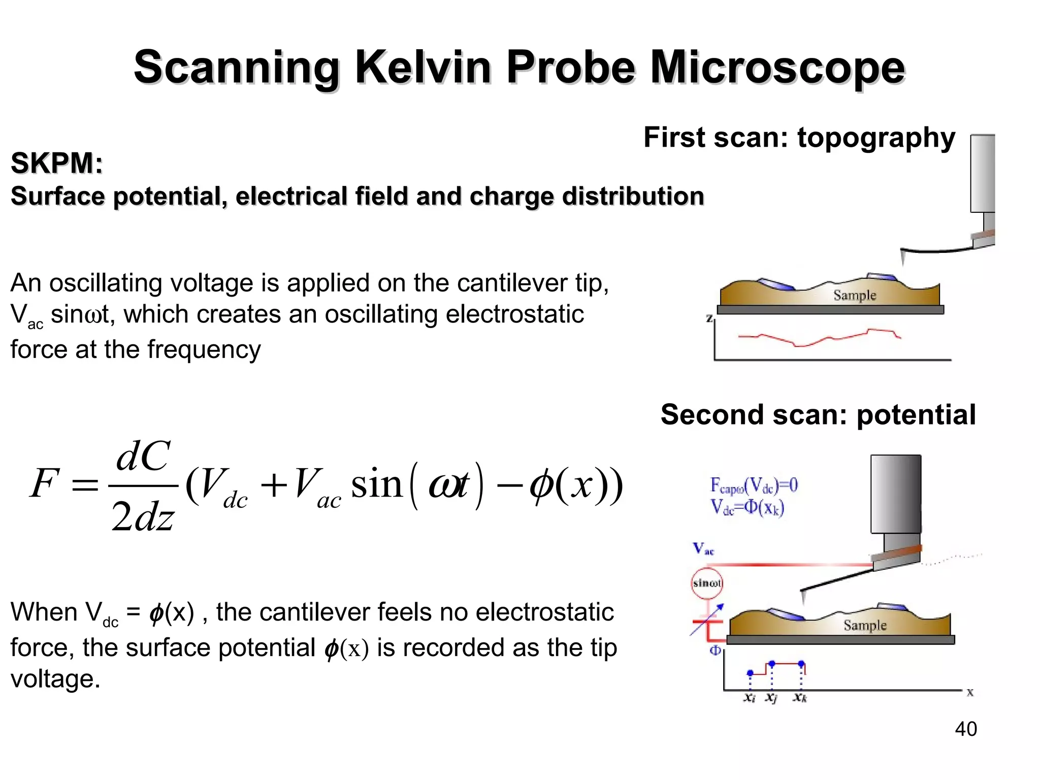
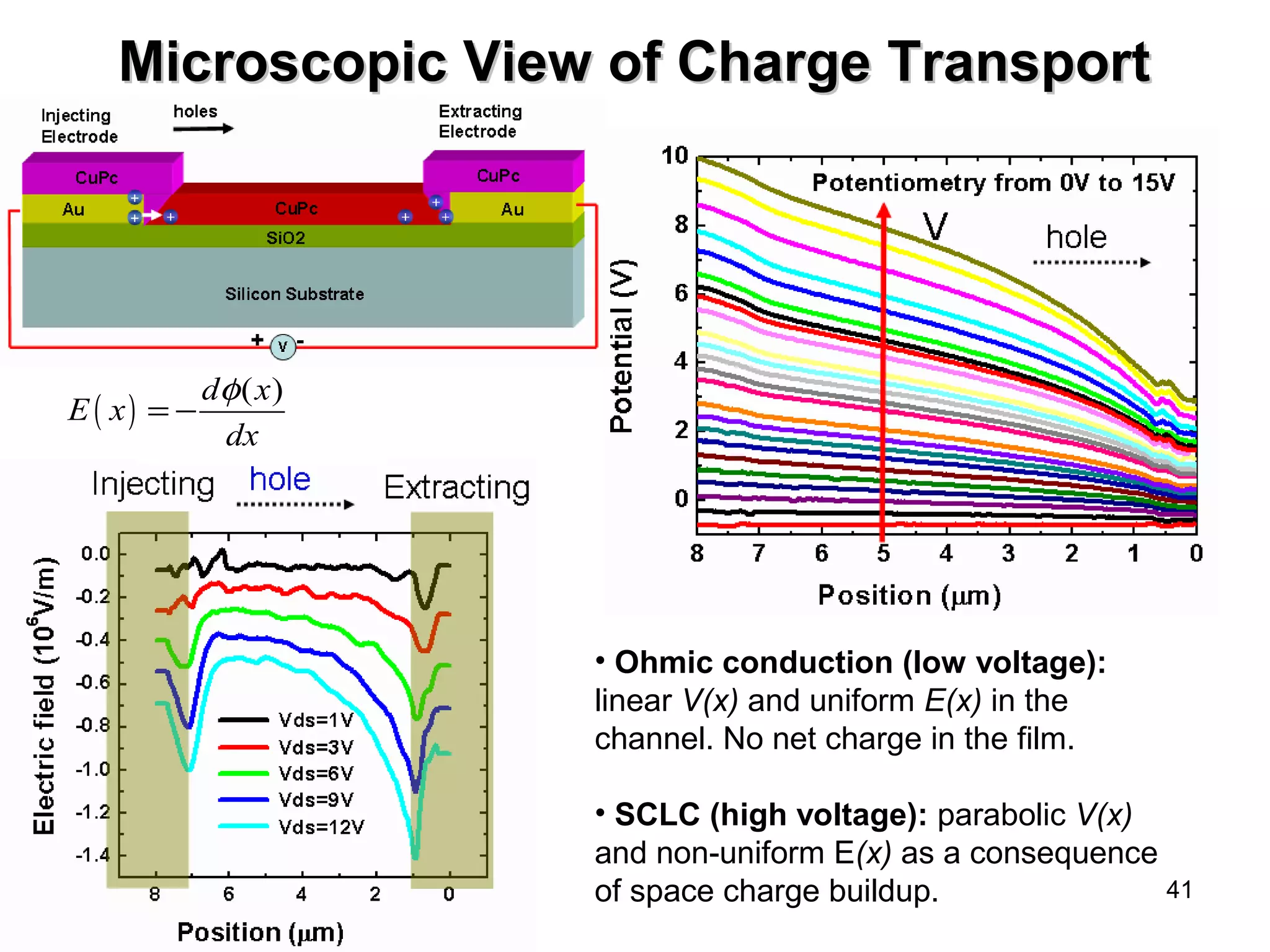
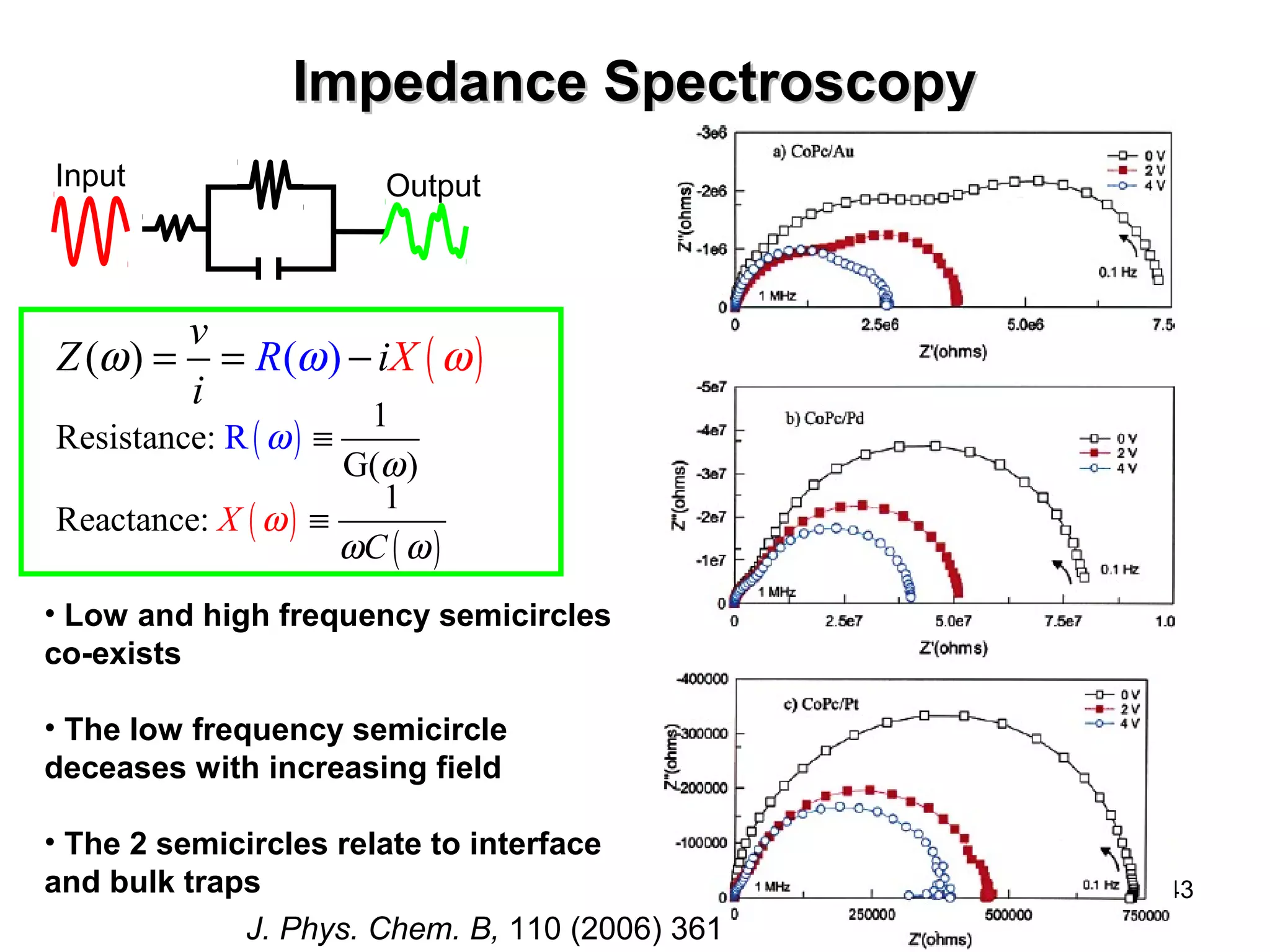
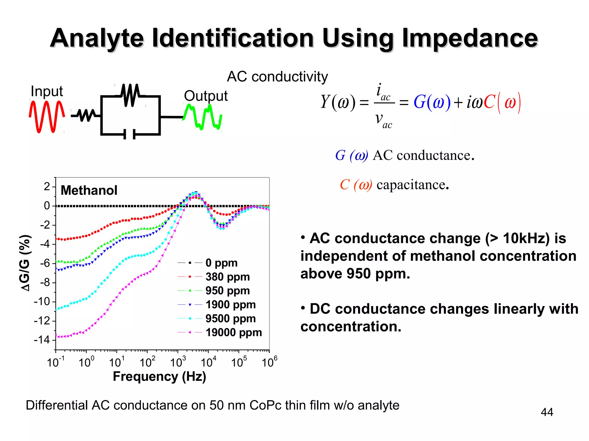
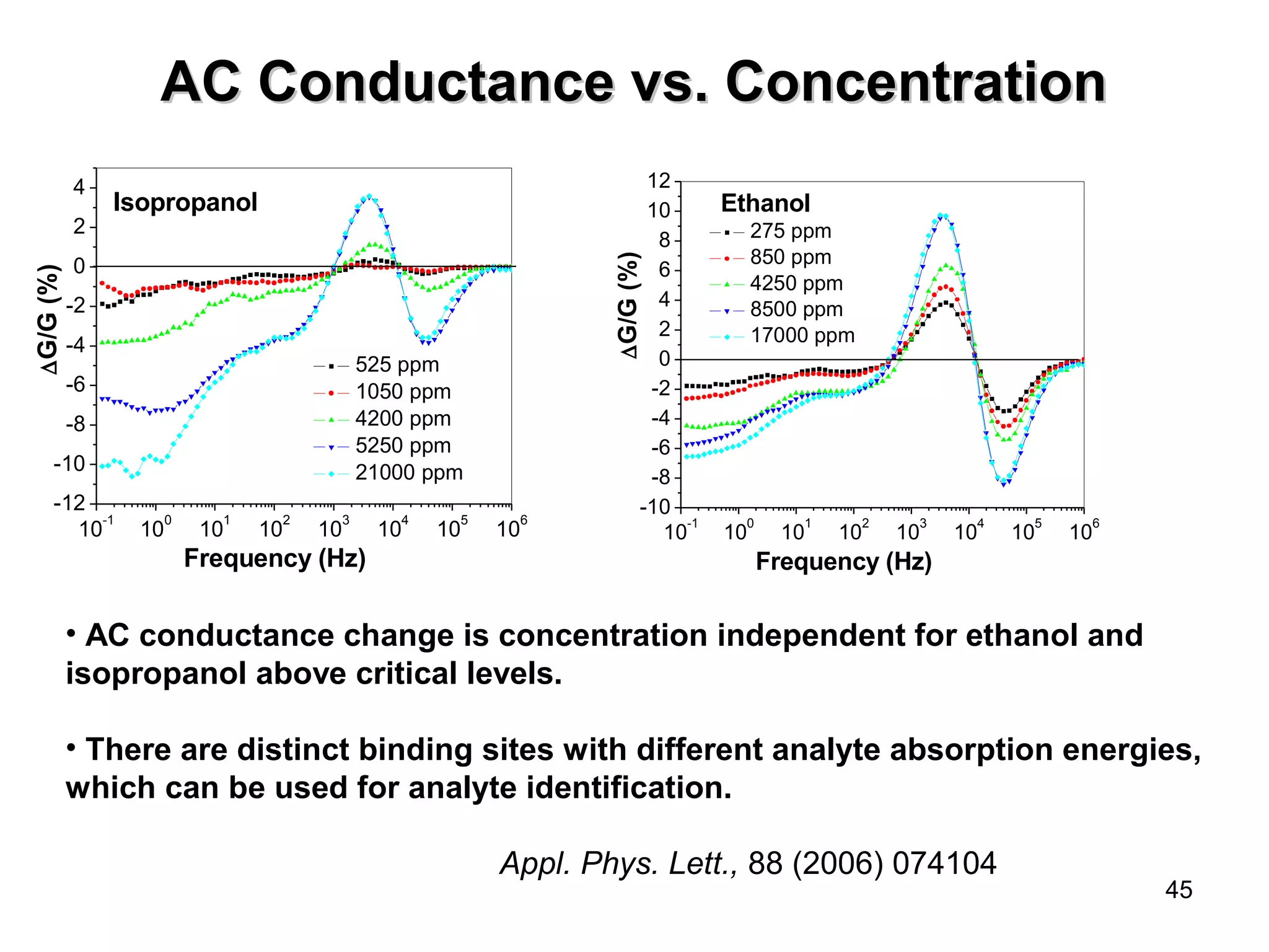
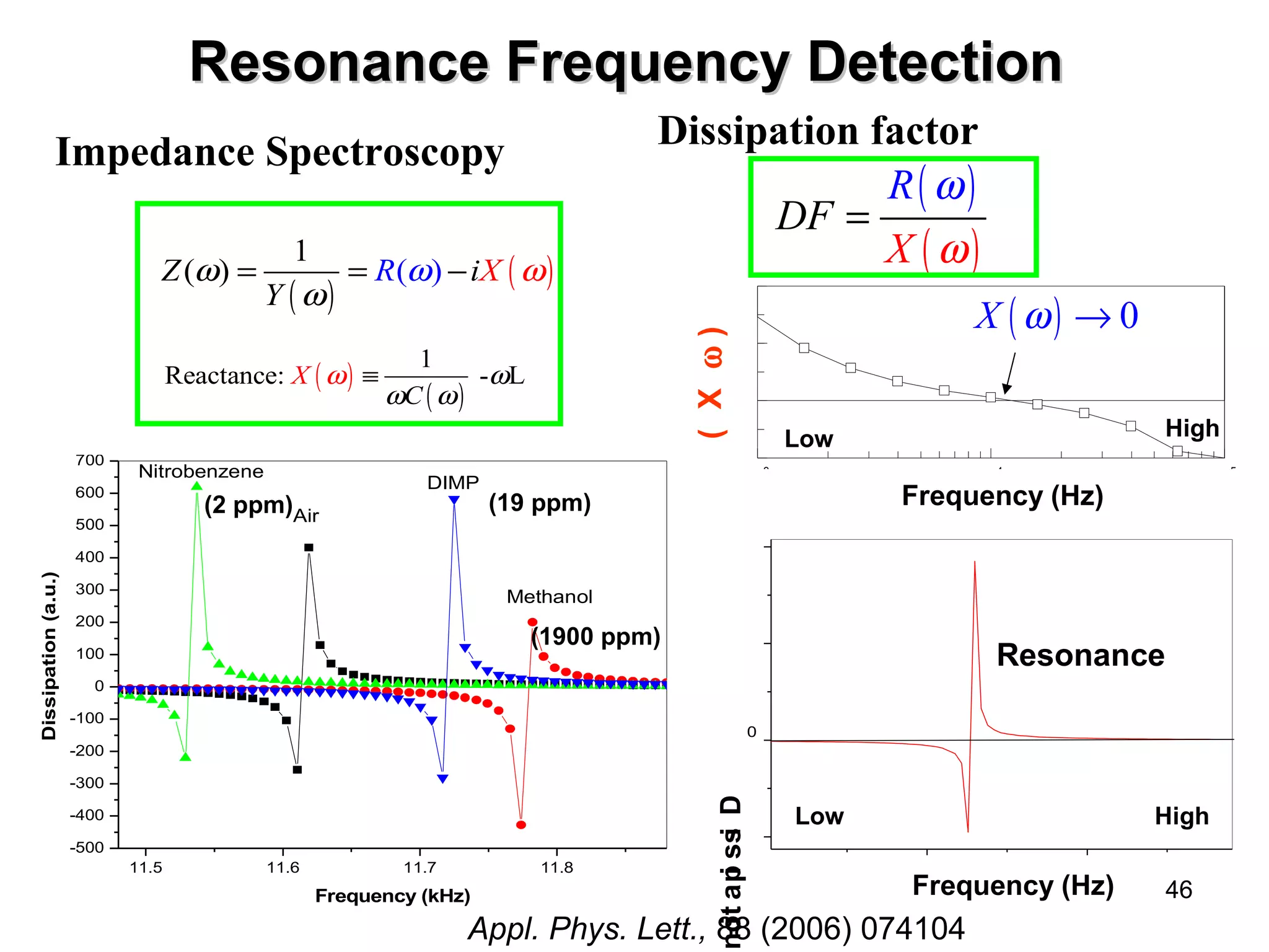
SlideShare a Scribd company logo
1 
CChhaarrggee TTrraannssppoorrtt aanndd CChheemmiiccaall 
SSeennssiinngg PPrrooppeerrttiieess ooff OOrrggaanniicc 
TThhiinn--ffiillmmss 
RRiicchhaarrdd YYaanngg 
Material Science & Engineering 
University of California, San Diego 
06/12/2007
2 
PPrroojjeecctt BBaacckkggrroouunndd 
AFOSR MURI: Integrated nanosensors for bio/chemical 
warfare and explosive agents detection. 
Organic thin-film chemical sensors 
• Chemiresistors 
• ChemFETs 
Design objectives 
• Sensitivity, Stability, Selectivity 
• Integration in sensor platform 
Conceptual design (2003)
3 
RReesseeaarrcchh AApppprrooaacchh 
Charge transport 
Device physics 
Chemical sensing
4 
RReessuullttss BBeeffoorree CCaannddiiddaaccyy 
• Analyte identification based on 
dispersive charge transport 
• Electrode independent chemical 
responses in SCLC regime 
2 Methanol 
0 
-2 
-4 
-6 
-8 
-10 
-12 
-14 
0 ppm 
380 ppm 
950 ppm 
1900 ppm 
9500 ppm 
19000 ppm 
10-1 100 101 102 103 104 105 106 
DG/G (%) 
Frequency (Hz) 
Appl. Phys. Lett., 88 (2006) 074104 J. Phys. Chem. B, 110 (2006) 361 
The above results were based on two-terminal chemiresistors.
5 
CChheemmiiccaallllyy SSeennssiittiivvee FFiieelldd--EEffffeecctt 
TTrraannssiissttoorrss 
gas 
Organic semiconductor 
thin-film 
S D 
+ + + + + + + + + 
Gate dielectric 
Silicon Substrate (n+ ) 
G 
Vg 
Id 
Vd 
Ground 
Advantages of ChemFETs as compared to chemiresistors: 
• High chemical sensitivity and stability 
• High electrical conductivity, therefore, may utilize very thin films
6 
DDeevviiccee FFaabbrriiccaattiioonn 
25 mm 
Photolithography, e-beam 
evaporation, lift-off process 
Organic thin-film deposited using 
molecular beam epitaxy 
• Film thickness: 5 - 50 nm 
• Growth rate: 0.2 – 1 Å/sec 
• Growth temperature: 20 – 200 0C 
SiO2 
Silicon Substrate (n+ ) 
Metal Phthalocyanine (MPc) 
Metal center: Cu, Co, Fe etc 
S 
G (Au) 
D
Low voltage operating ChemFET has been fabricated ( since Feb 2005). 
7 
DDeevviiccee CChhaarraacctteerriissttiiccss 
0 -1 -2 -3 -4 -5 
-3.0 
-2.5 
-2.0 
-1.5 
-1.0 
-0.5 
0.0 
Source-drain Voltage (V) 
( t nerr uC ni ar D m) A 
Gate Voltage = -5 V 
-4V 
-3 V 
-2 V 
0 V 
1, 2 V 
30 nm CuPc/ 50 nm SiO2 
• Low leakage current 
• Ideal FET behavior 
• Small threshold voltage 
• Low operating voltage
8 
CuPc OTFT Characteristics iinn LLiitteerraattuurree 
Appl. Phys. Lett. 69, 3066 (1996) J. Appl. Phys. 92, 6028 (2002) 
SiO2 thickness = 300 nm 
The operation voltages are 10 times too high for ChemFET applications.
Back gate process 
• Protect gate dielectric with PR 
• Dip into HF solution to remove 
9 
Fabrication IIssssuueess -- GGaattee LLeeaakkaaggee 
0 -2 -4 -6 -8 -10 
-14 
-12 
-10 
-8 
-6 
-4 
-2 
0 
Ig (mA) 
Vds (V) 
Vg 
-14 V 
+2 V 
50 nm SiO2 
Silicon Substrate (n+ ) 
Au 
G (Au) 
Au 
Gate leakage problem persisted in first 3 months 
backside SiO2 
• E-beam evaporation of Au 
Leakage sources and solutions: 
• Defective gate oxide: solved by careful growth and inspection 
• PR erosion by HF during backside SiO2 etching: solved by 
developing BOE etching
10 
Fabrication IIssssuuee -- CCoonnttaacctt RReessiissttaannccee 
Contact resistance limits current injection 
-1 V 
0 -2 -4 -6 -8 -10 
-1.4 
-1.2 
-1.0 
-0.8 
-0.6 
-0.4 
-0.2 
0.0 
Ids (mA) 
Vds (V) 
50 nm CuPc 
Vg = -14 V 
-10 V 
-8 V 
-6 V 
-4 V 
-2 V 
0 V 
2 V 
Source and solution: 
• Residual PR forms hole injection blocking layer: solved by 
developing cleaning procedure (three cycles of ultrasonication in 
trichloroethylene/ acetone/ isopropyl alcohol)) 
Residual PR
-2 V/step 
11 
DDeevviiccee SSccaalliinngg 
-6 7.5 micron channel 
-12 10 micron channel 
-10 
-8 
A) 
m(Current 0 -2 -4 -6 -8 -10 
Drain Source-Drain Voltage (V) -5 
-4 
-3 
-2 
-1 
0 
0 -2 -4 -6 -8 -10 
-6 
-4 
-2 
0 
-6 15 micron channel 
0 -2 -4 -6 -8 -10 
-5 
-4 
-3 
-2 
-1 
0 
-6 20 micron channel 
0 -2 -4 -6 -8 -10 
-5 
-4 
-3 
-2 
-1 
0 
Vgs = -10 V 
Vgs = +4 V 
nw/L=20,400 +/-1,200 nw/L=30,300 
nw/L=14,666 nw/L=15,000 
25ML CuPc Thin-films
12 
LLiinneeaarr SSccaalliinngg ooff CCuurrrreenntt wwiitthh CChhaannnneell 
Saturated region: V Vg = -8 V ds = -10 V 
Vg = -6 V 
Linear fits with R > 0.9 
I W C V 
( )2 
= m V - 
d,sat 2 i g t 
5 10 15 20 25 
-80 
-70 
-60 
-50 
-40 
-30 
-20 
-10 
Vg = -4 V 
IDS/(nW) (mA*mm) 
Channel Length (mm) 
L 
LLeennggtthh
Charge Transport iinn OOrrggaanniicc TTrraannssiissttoorrss 
E 
kT 
m = m q = m exp æç - a 
ö¸ eff 
0 0 è ø m= effective mobility 
eff13 
p-type organic semiconductor 
Delocalized conduction band 
+ Localized 
states 
EF 
+ + 
Delocalized valence band 
Multiple trapping and release (MTR) 
Transport in delocalized band 
Trapping and release 
G. Horowitz, M. E. Hajlaoui, and R. Hajlaoui, 
J. Appl. Phys. 87, 4456 (2000). 
m0= free carrier mobility 
q= free to total charge ratio 
Ea = trap activation energy 
Trap energy distribution determines the device characteristics
• Transconductance 
• Activation energy 
g g E 
k T 
14 
VVaarriiaabbllee TTeemmppeerraattuurree SSttuuddyy 
8 
d 
= ¶ 
¶ 
m Vds V 
g 
g I 
V =- 
0 exp( a ) 
m m 
B 
= - 
• The charge transport is thermally activated. 
• The activation energy depends on the gate voltage.
15 
Baseline DDrriifftt RReedduuccttiioonn iinn OOTTFFTTss 
-2 0 2 4 6 8 10 12 14 16 18 20 22 
1.0 
0.8 
0.6 
0.4 
Normalized Id 
Vg = -8 V, pulsing 
Vg = -4 V, static 
Time (hr) 
Vg = -8 V, static 
0 20 40 60 80 100 120 140 
1.05 
1.00 
0.95 
0.90 
0.85 
0.80 
0.75 
0.70 
Duty Cycle 
Normalized Id 
Time (minute) 
1% 
2% 
5% 
10% 
20% 
100% 
(a) 
threshold time 
100 1000 10000 
30 
25 
20 
15 
10 
5 
0 
Drift (%) 
Gate Bias Duration (ms) 
(b) 
• Static gate operation reduce drain 
current 40% in 20 h 
• Pulsed gating (0.1 Hz, 1% duty cycle) 
reduce the drift to less than 1% in 20 h 
• There is threshold pulse duration in the 
baseline drift
16 
Gate 
pulse 
train 
t 
PPuullsseedd GGaattiinngg OOppeerraattiioonn 
Ev 
Vg = 0 V 
Ec 
Ef 
SiO2 
Off 
State 
Ef 
Ev 
V SiO2 g = -8 V 
Ec 
tt 
On 
State 
•A pulse train from “off” to 
“on” state is applied. 
•Break lines represent trap 
states located near SiO2 
interface and in the bulk. 
•“Off State” – at flat band 
condition, no charge 
accumulation in the channel. 
•“On State” – holes 
accumulate at the dielectric 
interface. There is finite 
amount of time (tt) for the 
holes get trapped.
17 
BBaasseelliinnee DDrriifftt ttoo VVoollaattiillee VVaappoorrss 
-2 0 2 4 6 8 10 12 14 16 18 20 22 24 
1.0 
0.9 
0.8 
0.7 
0.6 
0.5 
0.4 
0.3 
(d) 
Normalized Drain Current 
Time (hr) 
(a) 
(b) 
1900 ppm methanol pulses (c) 
(a) 1% 0.1 Hz gate 
with methanol 
(b) static gate with 
methanol 
(c) static bias 
without 
methanol 
(d) 1900 ppm 
methanol 
pulses 
20 ML CuPc 
• Pulsed gating reduced the baseline drift to 0.09 + 0.016 %/h in exposure to 
15 methanol pulses. 
• Pulsed gating reduced the error in chemical response by 10%.
18 
Baseline DDrriifftt ttoo LLooww VVaappoorr PPrreessssuurree 
AAnnaallyytteess 
0 4 8 12 16 20 24 
1.00 
0.95 
0.90 
0.85 
0.80 
0.75 
Normalized Drain Current 
Constant flow gas pulses 
Time (h) 
(a) 
(b) 
(c) 
(a) 1% 0.1 Hz gate 
with 32 ppm 
DMMP 
(b) 1% 0.1 Hz gate 
with 19 ppm 
DIMP 
(c) Analyte pulse 
sequence 
• Chemical source of baseline drift has been tested with low vapor pressure 
analytes 
•There is 10% baseline drift due the tight binding of analytes
19 
CChheemmiiccaall DDrriifftt RReedduuccttiioonn 
(i) 
(ii) 
0 4 8 12 16 20 24 28 
30 
20 
10 
0.85 (b) 
(i) 
(ii) 
0 4 8 12 16 20 24 28 
0.90 
0.95 
1.00 
Normalized Id 
Time (h) 
0 
(iii) 
DIMP (ppm) 
(a) 
(iii) 
(a) 20% DIMP duty 
cycle 
(b) 15% DIMP duty 
cycle 
(c) 8% DIMP duty 
cycle 
• Even in the presence of very low volatility analytes, the drift can be reduced to 
zero by lowering the duty cycle of the analyte pulse.
Physical Structure BBaasseedd SSeennssiinngg MMooddeell 
20 
T. Someya, et. al. APL, 81, 3079 (2004) 
L. Torsi, et. al., Ana. Chem. 77, 308 A (2005) 
Assumptions 
• Film mobility is determined by traps located 
at grain boundary (GB) 
• Analytes adsorbed at grain surface change 
the GB barrier height EB and therefore 
change device mobility and threshold voltage 
Grain boundary model 
Limitations 
• No definite proof of trap state locating at 
GBs in organic films by SKPM 
• Weak correlation of chemical response with 
grain size 
• Electronic effect of oxygen doping 
ignored 
EB: Charge trapping barrier 
Polycrystalline pentacene film
21 
Scanning KKeellvviinn PPrroobbee MMiiccrroossccooppee 
Topography color scale: 20nm Potential color scale: 50mV 
220000 nnmm 
The potential drop between GBs is less than thermal energy. 
Data acquired by Xiaotian Zhou
22 
EEvviiddeenncceess ooff OOxxyyggeenn DDooppiinngg 
0 10 20 30 40 50 
2.2 
2.0 
1.8 
1.6 
-3.6 
-3.4 
-3.2 
-3.0 
-2.8 
• CuPc and F16CuPc sensing films out of vacuum are doped by oxygen 
• Oxygen is an acceptor-like dopant as it withdraws electron from 
phthalocyanines 
• Displacing oxygen reduces p-channel device current, while increases n-channel 
device current 
-2.6 
p-type 
p-channel Id (mA) 
n-channel Id(mA) 
Time (h) 
n-type
23 
Mo Electronic Moddeell ooff CChheemmiiccaall SSeennssiinngg 
• Organic sensing films are doped by chemisorbed oxygen once 
outside of vacuum. 
adsorption charge transfer Ionization 
k1 k2 + - k3 - + 
2 2 2 2 MPc + O ؾ® MPc-O ؾ®MPcd -Od ؾ®MPc-O +h 
• The surface layer has higher dopant concentration. 
SiO2 Air O2 
Si CuPc Air 
Ef - 
x0 
Ec 
Ev 
“delta-doping” 
• Chemical analytes adsorption on film surface has 2 effects: 
2 2 O /O 
s j 
– Surface doping level change due to oxygen displacement 
– Trapping energy change due to new energy states formed by analyte
24 
CChheemmiiccaall SSeennssiinngg MMeecchhaanniissmmss 
1.39 
1.38 
1.37 
1.36 
1.35 
n-channel 
Abs (Id) (mA) Time (h) 
-2 0 2 4 6 8 1012141618202224262830 
1.50 
1.45 
1.40 
1.35 
1.30 
1.25 
1.20 
0 60 120 180 
1.34 
I(mA) 
MeOH (1520 ppm) 
p-channel 
DMMP (68 ppm) 
DI
25 
TThhee EExxppoonneennttiiaall DDeeccaayyss 
-1.015 
-1.020 
-1.025 
-1.030 
-1.035 
-1.040 
0 2000 4000 6000 8000 10000 12000 
1.46 
1.44 
1.42 
1.40 
1.38 
1.36 
1.34 
Equation: y = A1*exp(-x/t1) + y0 
Weighting: 
y No weighting 
Chi^2/DoF = 2.1604E-6 
R^2 = 0.9964 
y0 1.33026 ±0.0006 
A1 0.11914 ±0.00048 
t1 7084.0095 ±73.686 
(a). n-channel: DMMP 
0 2000 4000 6000 8000 10000 12000 
-1.045 
(b). p-channel: DMMP 
Equation: y = A1*exp(-x/t1) + y0 
Weighting: 
y No weighting 
Chi^2/DoF = 1.3636E-7 
R^2 = 0.99732 
y0 -1.04583 ±0.0001 
A1 0.03262 ±0.00008 
t1 5736.22502 ±42.75252 
0 2000 4000 6000 
1.39 
1.38 
1.38 
1.37 
1.37 
1.36 
1.36 
1.35 
1.35 
Equation: y = A1*exp(-x/t1) + A2*exp(-x/t2) + y0 
Weighting: 
y No weighting 
Chi^2/DoF = 8.5004E-7 
R^2 = 0.99005 
y0 1.35052 ±0.00026 
A1 -0.01143 ±0.00066 
t1 57.13782 ±5.90263 
A2 0.03778 ±0.0002 
t2 2331.16822 ±44.41452 
(c). n-channel: MeOH 
Id (t) (mA) 
-0.99 
-1.00 
-1.01 
-1.02 
-1.03 
-1.04 
Time (second) 
raw data 
Exponetial fit 
0 2000 4000 6000 
-1.05 
(d). p-channel: MeOH 
Equation: y = A1*exp(-x/t1) + A2*exp(-x/t2) + y0 
Weighting: 
y No weighting 
Chi^2/DoF = 1.5898E-7 
R^2 = 0.99774 
y0 -1.04404 ±0.00007 
A1 0.04283 ±0.00025 
t1 189.38934 ±2.13073 
A2 0.01364 ±0.00019 
t2 1622.09746 ±43.98648
26 
Concentration DDeeppeeddeennddeenntt 
0 2 4 6 8 10 12 14 16 18 
1.46 
1.44 
1.42 
1.40 
1.38 
1.36 
50 
40 
30 
20 
10 
0 
Drain Current (mA) 
Time (h) 
Conc. (ppm) 
(a). n-channel: DMMP 
-2 0 2 4 6 8 10 12 14 16 18 
-1.06 
-1.05 
-1.05 
-1.04 
-1.04 
-1.03 
-1.03 
-1.02 
0 
10 
20 
30 
40 
50 
Drain Current (mA) 
Time (h) 
Conc. (ppm) 
(b). p-channel: DMMP 
n-channel 
0 10 20 30 40 50 60 
105 
90 
75 
60 
45 
30 
15 
0 
p-channel 
D I (nA) 
Concentration (ppm) 
1 exp b d I E S 
= D = - æ- ö I c çè kT 
ø¸
27 
BBiinnddiinngg ttoo aa WWeeaakk BBiinnddeerr 
p-channel 
0 500 1000 1500 
75 
60 
45 
30 
15 
0 
n-channel 
D I (nA) 
Concentration (ppm) 
2000 
1500 
1000 
500 
0 
0 
500 
1000 
1500 
2000 
1.40 
1.38 
1.36 
-1.46 (b). n-channel 
0 2 4 6 8 10 12 
-1.44 
-1.42 
-1.40 
-1.38 
-1.36 
0 2 4 6 8 10 12 
1.34 
Concentration (ppm) 
(a). n-channel 
Time (h) 
Drain Current (mA)
28 
UUllttrraasseennssiittiivvee SSeennssoorr DDeessiiggnn 
Merge the 2 interfaces: ultrasensitive ChemFET design 
In conventional OTFT sensors (> 10 nm), the chemical sensing and 
charge transport interfaces are separated.
29 
Chemical RReessppoonnssee CCoommppaarriissoonn 
4 ML CoPc 
DIMP Air NBMeOH 50 ML CoPc 
0 2 4 6 8 10 12 14 16 18 20 22 24 26 28 30 
-16 
-14 
-12 
-10 
-8 
-6 
-4 
-2 
-10 
-8 
-6 
-4 
-2 
12 TE 
DIMP 
/1.9 
NB 
/0.35 
0 2 4 6 8 10 12 14 16 18 20 22 24 26 28 30 
Appl. Phys. Lett., In Press 
8 
4 
0 
/44 
EA 
/150 
MeOH 
Conc (ppm) 
Time (h) 
MeOH 
/190 
Air 
0 
EA TE 
Response (%) 
0 2 4 6 8 10 12 14 16 18 20 22 24 26 28 30 
0 
EA TE Air DIMP NB
30 
S Chemical Seennssiittiivviittyy EEnnhhaanncceemmeenntt 
Sensitivity enhancement has been observed on all 5 analytes. 
0 exp a E 
- = æ ö è ç kT 
¸ ø 
m m 
m 0 is related to carrier density 
Ea is the trap energy at 
CoPc/SiO2 interface 
0 1 2 3 4 
16 
14 
12 
10 
8 
6 
4 
2 
0 
Ethyl 
acetate 
2.2 
Sensitivity Enhancement 
Dipole Moment (Debye) 
Toluene 
1.7 
MeOH 
4.0 
Nitrobenzene 
15.8 
DIMP 
3.62 
Effective field-effect mobility 
In the ultrathin device, the air/CoPc and CoPc/SiO2 interfaces are so 
close that analytes affect both carrier density and trap energy.
Nitrobenzene 
Simulant for TNT 
31 
Detection ooff NNiittrroobbeennzzeennee VVaappoorrss 
1.0 0 1 2 3 4 5 6 7 8 9 10 11 12 
0 1 2 3 4 5 6 7 8 9 10 11 12 
-2.61 
Id (mA) 
-2.70 
1.0 
0.5 
0.0 
Flow Rate (sccm) 
Time (hr) 
0.1 0.2 
0.6 
0.8 
-2.79 
Time (hr) 
Vg = - 8 V 
Vds = -4 V 
35 ppb 70 ppb 
210 ppb 
350 ppb 
280 ppb 
70 ppb nitrobenzene has been detected without a precentrator
2006 – 8 Pack 
with a blower in 
handheld package 
32 
2004 
PPrroojjeecctt EEvvoolluuttiioonn 
2005 
2006 – 6 Pack 
2004: Three parallel electrodes 
2005: Interdigitated electrodes 
2006: 6 pack ChemFET for an e-nose. 
2006: Handheld package. On-board integration of temperature, humidity 
sensors and current amplifier.
33 
WWiirreelleessss HHaannddhheelldd PPaacckkaaggee 
LLaabbvviieeww iinntteerrffaaccee 
VVaappoorr ssaammpplliinngg wwiitthh aa vvaaccuuuumm 
IInntteeggrraatteedd PPCCBB 
SSeennssoorr eenncclloossuurree 
BBlluuee ttooootthh ttrraannssmmiitttteerr
34 
SSuummmmaarryy 
• Process of low voltage operating and repeatable ChemFETs have 
been developed. 
• Trap states are found to dominate charge transport in organic 
transistors. 
• Pulsed gating technique has been developed to reduce drift to less 
than 0.1%/h in ChemFETs. 
• A ChemFET sensing model has been developed: gas adsorption on 
organic semiconductor surface changes both doping concentration 
and trap energy. 
• Ultrasensitive ChemFETs have been developed to detect explosive 
simulant at ppb level. 
• The project has evolved from discrete device to integrated circuits 
to handheld packages.
35 
AAcckknnoowwlleeddggeemmeennttss 
Committee Members: 
• Prof. Andrew Kummel (Chair) 
• Prof. Sungho Jin (Co-chair) 
• Prof. Yu-Hwa Lo 
• Prof. William Trogler 
• Prof. Edward Yu 
Collaborators (MSE, Chemistry, Physics) 
Jeongwon Park, Xiaotian Zhou, Corneliu Colesniuc, Dr. Karla Miller, 
Dr. Amos Sharoni and Dr. Thomas Gredig 
Undergrads (ECE, CSE and MAE) 
Ti, Tammy, Kate, Casey, Jordan, Sureel, Byron and Vince 
Funding from AFOSR MURI
36 
R Education/Reesseeaarrcchh BBaacckkggrroouunndd 
MM..SS.. 
SSuurrffaaccee CChheemmiissttrryy 
BB..SS.. 
CChheemmiiccaall EEnnggiinneeeerriinngg 
CChheemmiissttrryy 
RReesseeaarrcchh OOffffeerr 
IInnsstt.. ooff MMaatteerr.. RReess && EEnngg 
MM..SS.. 
AAddvvaanncceedd MMaatteerriiaallss 
MMaatteerriiaallss 
PPhh..DD.. 
MMaatteerriiaallss SScciieennccee && EEnnggiinneeeerriinngg
R Chemical Reessppoonnssee ooff pp aanndd nn CChhaannnneellss 
EEcc 
EEff EEDDIIMMPP 
EEooxxyyggeenn 
EEvv 
37 
p-channel n-channel 
-18 CuPc 50nm, L = 5 micron 
-16 
-14 
-12 
-10 
-8 
-6 
-4 
-2 
0 
2 
190 ppm DIMP 
-20 -15 -10 -5 0 5 
Drain Current (mA) 
Gate Voltage (V) 
air 
DIMP 
Vds = -6 V 
7 F16CuPc 50nm, L = 5 micron 
25 20 15 10 5 0 -5 
6 
5 
4 
3 
2 
1 
0 
Drain Current (mA) 
Gate Voltage (V) 
air 
DIMP 
Vds = +6 V 
CuPc F16CuPc 
EEcc 
EEff EEDDIIMMPP 
EEooxxyyggeenn 
EEvv 
Analyte adsorption changes free carrier concentration and trap energy.
0 2 4 6 8 10 
38 
RRoollee ooff OOxxyyggeenn iinn SSeennssiinngg 
2.0 
1.9 
1.8 
1.7 
1.6 
N(a). n-channel 2 
Drain Current (mA) Time (h) 
-2 0 2 4 6 8 10 12 14 16 18 20 
-2 0 2 4 6 8 10 12 14 16 18 20 
1.5 
1.4 
-1.2 
-1.1 
-1.0 
-0.9 
-0.8 
-0.7 
-0.6 
air (b). p-channel 
N2 
1.3 
air 
0 2 4 6 8 10 
1.7 
1.6 
1.5 
-1.1 
-1.0 
-0.9 
-0.8 
-0.7 
N2 
(b). p-channel 
air 
Drain Current (mA) 
Time (h) 
1.4 
N2 
air 
(a). n-channel 
NNoott ddiirreecctt ddiissppllaacceemmeenntt.. 
AA mmiixxttuurree ooff tthhee ccoo-- 
aaddssoorrppttiioonn aanndd rreemmoottee 
aaddssoorrppttiioonn
39 
Macroscopic VViieeww ooff CChhaarrggee TTrraannssppoorrtt 
•Low voltage region, Ohmic 
conduction 
= m V 
0 J N e 
d 
• High voltage region, space-charge 
limited conduction 
2 
3 
J = em V 
9 
8 d 
J = current density 
N0= thermal carrier concentration 
e = permittivity of material 
V = voltage bias 
d = film thickness
40 
Scanning KKeellvviinn PPrroobbee MMiiccrroossccooppee 
SSKKPPMM:: 
SSuurrffaaccee ppootteennttiiaall,, eelleeccttrriiccaall ffiieelldd aanndd cchhaarrggee ddiissttrriibbuuttiioonn 
An oscillating voltage is applied on the cantilever tip, 
Vac sinwt, which creates an oscillating electrostatic 
force at the frequency 
F dC V V t x 
( sin( ) ( )) 
= + w -f 
2 dz 
dc ac 
When Vdc = f (x) , the cantilever feels no electrostatic 
force, the surface potential f (x) is recorded as the tip 
voltage. 
First scan: topography 
Second scan: potential
41 
Microscopic VViieeww ooff CChhaarrggee TTrraannssppoorrtt 
E( x) = - d f 
(x) 
dx 
• Ohmic conduction (low voltage): 
linear V(x) and uniform E(x) in the 
channel. No net charge in the film. 
• SCLC (high voltage): parabolic V(x) 
and non-uniform E(x) as a consequence 
of space charge buildup.
• AAtt hhiigghh vvoollttaaggee,, cchheemmiiccaall rreessppoonnssee iiss iinnddeeppeennddeenntt ooff ccoonnttaacctt aanndd hhiissttoorryy 
• TThhee iinntteerrffaaccee ttrraappss aarree ffiilllleedd uupp tthhaatt ddoo nnoott aaffffeecctt cchheemmiiccaall sseennssiinngg 
42 
EElleeccttrrooddee IInnddeeppeennddeenntt CChheemmiiccaall 
RReessppoonnssee iinn SSCCLLCC RReeggiioonn 
J. Phys. Chem. B, 110 (2006) 361
43 
IImmppeeddaannccee SSppeeccttrroossccooppyy 
Input Output 
( ) v R( ) ( ) 
Z w = = w - iX w 
Resistance: R( ) 1 
Reactance: X 1 
J. Phys. Chem. B, 110 (2006) 361 
i 
G( ) 
w 
w 
º 
( w 
) º 
w C 
( w 
) 
• Low and high frequency semicircles 
co-exists 
• The low frequency semicircle 
deceases with increasing field 
• The 2 semicircles relate to interface 
and bulk traps
44 
Analyte Identification UUssiinngg IImmppeeddaannccee 
Input Output 
2 Methanol 
0 
-2 
-4 
-6 
-8 
-10 
-12 
-14 
AC conductivity 
0 ppm 
380 ppm 
950 ppm 
1900 ppm 
9500 ppm 
19000 ppm 
10-1 100 101 102 103 104 105 106 
DG/G (%) 
Frequency (Hz) 
Y i 
( w ) = ac = G ( w ) + iwC ( w 
) 
v 
ac 
G (w) AC conductance. 
C (w) capacitance. 
• AC conductance change (> 10kHz) is 
independent of methanol concentration 
above 950 ppm. 
• DC conductance changes linearly with 
concentration. 
Differential AC conductance on 50 nm CoPc thin film w/o analyte
45 
AC Conductance vvss.. CCoonncceennttrraattiioonn 
4 Isopropanol 
2 
0 
-2 
-4 
-6 
-8 
-10 
-12 
525 ppm 
1050 ppm 
4200 ppm 
5250 ppm 
21000 ppm 
10-1 100 101 102 103 104 105 106 
DG/G (%) 
Frequency (Hz) 
12 
10 
8 
6 
4 
2 
0 
-2 
-4 
-6 
-8 
-10 
Ethanol 
275 ppm 
850 ppm 
4250 ppm 
8500 ppm 
17000 ppm 
10-1 100 101 102 103 104 105 106 
DG/G (%) 
Frequency (Hz) 
• AC conductance change is concentration independent for ethanol and 
isopropanol above critical levels. 
• There are distinct binding sites with different analyte absorption energies, 
which can be used for analyte identification. 
Appl. Phys. Lett., 88 (2006) 074104
Low High 
46 
104 
Resonance FFrreeqquueennccyy DDeetteeccttiioonn 
Z( w ) 1 ( ) R ( ) i 
X 
( ) = = w - w 
Y 
w 
Reactance: X 1 - L 
( ) ( ) 
w º w 
wC w 
Dissipation factor 
R 
( w 
) 
DF 
= 
X 
( w 
) Impedance Spectroscopy 
(2 ppm) (19 ppm) 
Dissipation (a.u.) Frequency (kHz) 
11.5 11.6 11.7 11.8 
700 
600 
500 
400 
300 
200 
100 
0 
-100 
-200 
-300 
-400 
-500 
Air 
Methanol 
Nitrobenzene DIMP 
(1900 ppm) 
103 
103 104 105 
Frequency (Hz) 
X (w) 
-100000 
-50000 
0 
50000 
103 104 105 
Frequency (Hz) 
( X w ) 
Frequency (Hz) 
0 
X (w ) ®0 
Resonance 
Frequency (Hz) 
noit api ssi D 
Low High 
Appl. Phys. Lett., 88 (2006) 074104
47 
SSuummmmaarryy –– 22 TTeerrmmiinnaall DDeevviiccee 
• Charge transport in organic thin-film is Ohmic at low 
field and SCLC at high field. 
• Operating Chemiresistors in SCLC region gives contact 
independent chemical responses. 
• There are co-existence of low frequency and high 
frequency transport states in organic thin-film. 
• An impedance spectroscopy technique has been 
developed to identify chemical analytes based on 
dispersive charge transport.

More Related Content

What's hot

Carrier scattering and ballistic transport
Carrier scattering and ballistic transportCarrier scattering and ballistic transport
Carrier scattering and ballistic transport
RCC Institute of Information Technology
 
Dielectric Spectroscopy and Dielectric Permittivity Physical Nature
Dielectric Spectroscopy and Dielectric Permittivity Physical NatureDielectric Spectroscopy and Dielectric Permittivity Physical Nature
Dielectric Spectroscopy and Dielectric Permittivity Physical Nature
SSA KPI
 
L10 superconductivity
L10 superconductivityL10 superconductivity
L10 superconductivitymphilip1
 
Single Electron Transistor
Single Electron TransistorSingle Electron Transistor
Single Electron Transistor
RCC Institute of Information Technology
 
Brandt - Superconductors and Vortices at Radio Frequency Magnetic Fields
Brandt - Superconductors and Vortices at Radio Frequency Magnetic FieldsBrandt - Superconductors and Vortices at Radio Frequency Magnetic Fields
Brandt - Superconductors and Vortices at Radio Frequency Magnetic Fields
thinfilmsworkshop
 
Poster Superconductivity
Poster SuperconductivityPoster Superconductivity
Poster SuperconductivityJohn Guss
 
Case Study: Cyclic Voltametric Measurement
Case Study: Cyclic Voltametric MeasurementCase Study: Cyclic Voltametric Measurement
Case Study: Cyclic Voltametric Measurement
Hasnain Ali
 
Dielectric Spectroscopy in Time and Frequency Domain
Dielectric Spectroscopy in Time and Frequency DomainDielectric Spectroscopy in Time and Frequency Domain
Dielectric Spectroscopy in Time and Frequency Domain
Girish Gupta
 
Fermi surface and de haas van alphen effect ppt
Fermi surface and de haas van alphen effect pptFermi surface and de haas van alphen effect ppt
Fermi surface and de haas van alphen effect ppt
tedoado
 
high voltage engineering module1(EE369)-KTU
high voltage engineering module1(EE369)-KTUhigh voltage engineering module1(EE369)-KTU
high voltage engineering module1(EE369)-KTU
Asha Anu Kurian
 
CNT Ballistic Transistor
CNT Ballistic TransistorCNT Ballistic Transistor
CNT Ballistic Transistor
Tashfain Yousuf
 
The dynamical-casimir-effect-in-superconducting-microwave-circuits
The dynamical-casimir-effect-in-superconducting-microwave-circuitsThe dynamical-casimir-effect-in-superconducting-microwave-circuits
The dynamical-casimir-effect-in-superconducting-microwave-circuits
villa1451
 
Ajal electrostatics slides
Ajal electrostatics slidesAjal electrostatics slides
Ajal electrostatics slides
AJAL A J
 
Basic potential step and sweep methods
Basic potential step and sweep methodsBasic potential step and sweep methods
Basic potential step and sweep methods
Getachew Solomon
 
ELECTRODYNAMIC FIELDS
ELECTRODYNAMIC FIELDSELECTRODYNAMIC FIELDS
ELECTRODYNAMIC FIELDS
Karthik Kathan
 
Ch20 Electromagnetic Induction
Ch20 Electromagnetic InductionCh20 Electromagnetic Induction
Ch20 Electromagnetic Induction
Rohit Mohd
 

What's hot (20)

Carrier scattering and ballistic transport
Carrier scattering and ballistic transportCarrier scattering and ballistic transport
Carrier scattering and ballistic transport
 
Dielectric Spectroscopy and Dielectric Permittivity Physical Nature
Dielectric Spectroscopy and Dielectric Permittivity Physical NatureDielectric Spectroscopy and Dielectric Permittivity Physical Nature
Dielectric Spectroscopy and Dielectric Permittivity Physical Nature
 
L10 superconductivity
L10 superconductivityL10 superconductivity
L10 superconductivity
 
Single Electron Transistor
Single Electron TransistorSingle Electron Transistor
Single Electron Transistor
 
Brandt - Superconductors and Vortices at Radio Frequency Magnetic Fields
Brandt - Superconductors and Vortices at Radio Frequency Magnetic FieldsBrandt - Superconductors and Vortices at Radio Frequency Magnetic Fields
Brandt - Superconductors and Vortices at Radio Frequency Magnetic Fields
 
Part 1:Electrostatics
Part 1:ElectrostaticsPart 1:Electrostatics
Part 1:Electrostatics
 
Poster Superconductivity
Poster SuperconductivityPoster Superconductivity
Poster Superconductivity
 
Case Study: Cyclic Voltametric Measurement
Case Study: Cyclic Voltametric MeasurementCase Study: Cyclic Voltametric Measurement
Case Study: Cyclic Voltametric Measurement
 
Squid2
Squid2Squid2
Squid2
 
Dielectric Spectroscopy in Time and Frequency Domain
Dielectric Spectroscopy in Time and Frequency DomainDielectric Spectroscopy in Time and Frequency Domain
Dielectric Spectroscopy in Time and Frequency Domain
 
Fermi surface and de haas van alphen effect ppt
Fermi surface and de haas van alphen effect pptFermi surface and de haas van alphen effect ppt
Fermi surface and de haas van alphen effect ppt
 
high voltage engineering module1(EE369)-KTU
high voltage engineering module1(EE369)-KTUhigh voltage engineering module1(EE369)-KTU
high voltage engineering module1(EE369)-KTU
 
AFMC Physics 2006
AFMC Physics  2006AFMC Physics  2006
AFMC Physics 2006
 
Icops 2011 June
Icops 2011 JuneIcops 2011 June
Icops 2011 June
 
CNT Ballistic Transistor
CNT Ballistic TransistorCNT Ballistic Transistor
CNT Ballistic Transistor
 
The dynamical-casimir-effect-in-superconducting-microwave-circuits
The dynamical-casimir-effect-in-superconducting-microwave-circuitsThe dynamical-casimir-effect-in-superconducting-microwave-circuits
The dynamical-casimir-effect-in-superconducting-microwave-circuits
 
Ajal electrostatics slides
Ajal electrostatics slidesAjal electrostatics slides
Ajal electrostatics slides
 
Basic potential step and sweep methods
Basic potential step and sweep methodsBasic potential step and sweep methods
Basic potential step and sweep methods
 
ELECTRODYNAMIC FIELDS
ELECTRODYNAMIC FIELDSELECTRODYNAMIC FIELDS
ELECTRODYNAMIC FIELDS
 
Ch20 Electromagnetic Induction
Ch20 Electromagnetic InductionCh20 Electromagnetic Induction
Ch20 Electromagnetic Induction
 

Similar to ChemFET fabrication, device physics and sensing mechanism

Charged-Current Pion Production in T2K
Charged-Current Pion Production in T2KCharged-Current Pion Production in T2K
Charged-Current Pion Production in T2K
Son Cao
 
HDR Vincent Agache Defense
HDR Vincent Agache DefenseHDR Vincent Agache Defense
HDR Vincent Agache Defensevince3859
 
SFH6916_08 - Datasheet - VISHAY
SFH6916_08 - Datasheet - VISHAYSFH6916_08 - Datasheet - VISHAY
SFH6916_08 - Datasheet - VISHAY
MarioFarias18
 
Design and implementation of cyclo converter for high frequency applications
Design and implementation of cyclo converter for high frequency applicationsDesign and implementation of cyclo converter for high frequency applications
Design and implementation of cyclo converter for high frequency applications
cuashok07
 
Atomic Layer Deposition: a process technology for transparent conducting oxides
Atomic Layer Deposition: a process technology for transparent conducting oxidesAtomic Layer Deposition: a process technology for transparent conducting oxides
Atomic Layer Deposition: a process technology for transparent conducting oxides
cdtpv
 
Original Opto NEC8701 PS8701 8701 SOP-5 New
Original Opto NEC8701 PS8701 8701 SOP-5 NewOriginal Opto NEC8701 PS8701 8701 SOP-5 New
Original Opto NEC8701 PS8701 8701 SOP-5 New
AUTHELECTRONIC
 
51 MLD STP BY C-TECH
51 MLD STP BY C-TECH51 MLD STP BY C-TECH
51 MLD STP BY C-TECHVenu M
 
Trends in Future CommunicationsInternational Workshop - Renato Rabelo
Trends in Future CommunicationsInternational Workshop - Renato RabeloTrends in Future CommunicationsInternational Workshop - Renato Rabelo
Trends in Future CommunicationsInternational Workshop - Renato RabeloCPqD
 
MOCVD半導體製程即時監控系統
MOCVD半導體製程即時監控系統MOCVD半導體製程即時監控系統
MOCVD半導體製程即時監控系統
CHENHuiMei
 
Libo proton linac booster presentation
Libo proton linac booster presentationLibo proton linac booster presentation
Libo proton linac booster presentation
Paolo Berra
 
Mag flow
Mag flowMag flow
Demonstrating Quantum Speed-Up with a Two-Transmon Quantum Processor Ph.D. d...
Demonstrating Quantum Speed-Up  with a Two-Transmon Quantum Processor Ph.D. d...Demonstrating Quantum Speed-Up  with a Two-Transmon Quantum Processor Ph.D. d...
Demonstrating Quantum Speed-Up with a Two-Transmon Quantum Processor Ph.D. d...
Andreas Dewes
 
First results from the full-scale prototype for the Fluorescence detector Arr...
First results from the full-scale prototype for the Fluorescence detector Arr...First results from the full-scale prototype for the Fluorescence detector Arr...
First results from the full-scale prototype for the Fluorescence detector Arr...
Toshihiro FUJII
 
Electrical Capacitance Volume Tomography
Electrical Capacitance Volume Tomography Electrical Capacitance Volume Tomography
Electrical Capacitance Volume Tomography
tech4imaging
 
Original Opto PS9151-V-F3-AX 9151 SOP-5 New
Original Opto PS9151-V-F3-AX 9151 SOP-5 NewOriginal Opto PS9151-V-F3-AX 9151 SOP-5 New
Original Opto PS9151-V-F3-AX 9151 SOP-5 New
authelectroniccom
 

Similar to ChemFET fabrication, device physics and sensing mechanism (20)

Charged-Current Pion Production in T2K
Charged-Current Pion Production in T2KCharged-Current Pion Production in T2K
Charged-Current Pion Production in T2K
 
HDR Vincent Agache Defense
HDR Vincent Agache DefenseHDR Vincent Agache Defense
HDR Vincent Agache Defense
 
SFH6916_08 - Datasheet - VISHAY
SFH6916_08 - Datasheet - VISHAYSFH6916_08 - Datasheet - VISHAY
SFH6916_08 - Datasheet - VISHAY
 
Gupta Roy MS Thesis Defense
Gupta Roy MS Thesis DefenseGupta Roy MS Thesis Defense
Gupta Roy MS Thesis Defense
 
Design and implementation of cyclo converter for high frequency applications
Design and implementation of cyclo converter for high frequency applicationsDesign and implementation of cyclo converter for high frequency applications
Design and implementation of cyclo converter for high frequency applications
 
Thesis presentation
Thesis presentationThesis presentation
Thesis presentation
 
Atomic Layer Deposition: a process technology for transparent conducting oxides
Atomic Layer Deposition: a process technology for transparent conducting oxidesAtomic Layer Deposition: a process technology for transparent conducting oxides
Atomic Layer Deposition: a process technology for transparent conducting oxides
 
TRANSISTORES
TRANSISTORESTRANSISTORES
TRANSISTORES
 
Original Opto NEC8701 PS8701 8701 SOP-5 New
Original Opto NEC8701 PS8701 8701 SOP-5 NewOriginal Opto NEC8701 PS8701 8701 SOP-5 New
Original Opto NEC8701 PS8701 8701 SOP-5 New
 
Lab sheet
Lab sheetLab sheet
Lab sheet
 
51 MLD STP BY C-TECH
51 MLD STP BY C-TECH51 MLD STP BY C-TECH
51 MLD STP BY C-TECH
 
Trends in Future CommunicationsInternational Workshop - Renato Rabelo
Trends in Future CommunicationsInternational Workshop - Renato RabeloTrends in Future CommunicationsInternational Workshop - Renato Rabelo
Trends in Future CommunicationsInternational Workshop - Renato Rabelo
 
Meph 569 final exam- 032
Meph 569 final exam- 032Meph 569 final exam- 032
Meph 569 final exam- 032
 
MOCVD半導體製程即時監控系統
MOCVD半導體製程即時監控系統MOCVD半導體製程即時監控系統
MOCVD半導體製程即時監控系統
 
Libo proton linac booster presentation
Libo proton linac booster presentationLibo proton linac booster presentation
Libo proton linac booster presentation
 
Mag flow
Mag flowMag flow
Mag flow
 
Demonstrating Quantum Speed-Up with a Two-Transmon Quantum Processor Ph.D. d...
Demonstrating Quantum Speed-Up  with a Two-Transmon Quantum Processor Ph.D. d...Demonstrating Quantum Speed-Up  with a Two-Transmon Quantum Processor Ph.D. d...
Demonstrating Quantum Speed-Up with a Two-Transmon Quantum Processor Ph.D. d...
 
First results from the full-scale prototype for the Fluorescence detector Arr...
First results from the full-scale prototype for the Fluorescence detector Arr...First results from the full-scale prototype for the Fluorescence detector Arr...
First results from the full-scale prototype for the Fluorescence detector Arr...
 
Electrical Capacitance Volume Tomography
Electrical Capacitance Volume Tomography Electrical Capacitance Volume Tomography
Electrical Capacitance Volume Tomography
 
Original Opto PS9151-V-F3-AX 9151 SOP-5 New
Original Opto PS9151-V-F3-AX 9151 SOP-5 NewOriginal Opto PS9151-V-F3-AX 9151 SOP-5 New
Original Opto PS9151-V-F3-AX 9151 SOP-5 New
 

Recently uploaded

Runway Orientation Based on the Wind Rose Diagram.pptx
Runway Orientation Based on the Wind Rose Diagram.pptxRunway Orientation Based on the Wind Rose Diagram.pptx
Runway Orientation Based on the Wind Rose Diagram.pptx
SupreethSP4
 
一比一原版(UofT毕业证)多伦多大学毕业证成绩单如何办理
一比一原版(UofT毕业证)多伦多大学毕业证成绩单如何办理一比一原版(UofT毕业证)多伦多大学毕业证成绩单如何办理
一比一原版(UofT毕业证)多伦多大学毕业证成绩单如何办理
ydteq
 
Hierarchical Digital Twin of a Naval Power System
Hierarchical Digital Twin of a Naval Power SystemHierarchical Digital Twin of a Naval Power System
Hierarchical Digital Twin of a Naval Power System
Kerry Sado
 
一比一原版(SFU毕业证)西蒙菲莎大学毕业证成绩单如何办理
一比一原版(SFU毕业证)西蒙菲莎大学毕业证成绩单如何办理一比一原版(SFU毕业证)西蒙菲莎大学毕业证成绩单如何办理
一比一原版(SFU毕业证)西蒙菲莎大学毕业证成绩单如何办理
bakpo1
 
Hybrid optimization of pumped hydro system and solar- Engr. Abdul-Azeez.pdf
Hybrid optimization of pumped hydro system and solar- Engr. Abdul-Azeez.pdfHybrid optimization of pumped hydro system and solar- Engr. Abdul-Azeez.pdf
Hybrid optimization of pumped hydro system and solar- Engr. Abdul-Azeez.pdf
fxintegritypublishin
 
English lab ppt no titlespecENG PPTt.pdf
English lab ppt no titlespecENG PPTt.pdfEnglish lab ppt no titlespecENG PPTt.pdf
English lab ppt no titlespecENG PPTt.pdf
BrazilAccount1
 
Top 10 Oil and Gas Projects in Saudi Arabia 2024.pdf
Top 10 Oil and Gas Projects in Saudi Arabia 2024.pdfTop 10 Oil and Gas Projects in Saudi Arabia 2024.pdf
Top 10 Oil and Gas Projects in Saudi Arabia 2024.pdf
Teleport Manpower Consultant
 
ethical hacking in wireless-hacking1.ppt
ethical hacking in wireless-hacking1.pptethical hacking in wireless-hacking1.ppt
ethical hacking in wireless-hacking1.ppt
Jayaprasanna4
 
NO1 Uk best vashikaran specialist in delhi vashikaran baba near me online vas...
NO1 Uk best vashikaran specialist in delhi vashikaran baba near me online vas...NO1 Uk best vashikaran specialist in delhi vashikaran baba near me online vas...
NO1 Uk best vashikaran specialist in delhi vashikaran baba near me online vas...
Amil Baba Dawood bangali
 
ethical hacking-mobile hacking methods.ppt
ethical hacking-mobile hacking methods.pptethical hacking-mobile hacking methods.ppt
ethical hacking-mobile hacking methods.ppt
Jayaprasanna4
 
RAT: Retrieval Augmented Thoughts Elicit Context-Aware Reasoning in Long-Hori...
RAT: Retrieval Augmented Thoughts Elicit Context-Aware Reasoning in Long-Hori...RAT: Retrieval Augmented Thoughts Elicit Context-Aware Reasoning in Long-Hori...
RAT: Retrieval Augmented Thoughts Elicit Context-Aware Reasoning in Long-Hori...
thanhdowork
 
CME397 Surface Engineering- Professional Elective
CME397 Surface Engineering- Professional ElectiveCME397 Surface Engineering- Professional Elective
CME397 Surface Engineering- Professional Elective
karthi keyan
 
power quality voltage fluctuation UNIT - I.pptx
power quality voltage fluctuation UNIT - I.pptxpower quality voltage fluctuation UNIT - I.pptx
power quality voltage fluctuation UNIT - I.pptx
ViniHema
 
road safety engineering r s e unit 3.pdf
road safety engineering  r s e unit 3.pdfroad safety engineering  r s e unit 3.pdf
road safety engineering r s e unit 3.pdf
VENKATESHvenky89705
 
MCQ Soil mechanics questions (Soil shear strength).pdf
MCQ Soil mechanics questions (Soil shear strength).pdfMCQ Soil mechanics questions (Soil shear strength).pdf
MCQ Soil mechanics questions (Soil shear strength).pdf
Osamah Alsalih
 
WATER CRISIS and its solutions-pptx 1234
WATER CRISIS and its solutions-pptx 1234WATER CRISIS and its solutions-pptx 1234
WATER CRISIS and its solutions-pptx 1234
AafreenAbuthahir2
 
CFD Simulation of By-pass Flow in a HRSG module by R&R Consult.pptx
CFD Simulation of By-pass Flow in a HRSG module by R&R Consult.pptxCFD Simulation of By-pass Flow in a HRSG module by R&R Consult.pptx
CFD Simulation of By-pass Flow in a HRSG module by R&R Consult.pptx
R&R Consult
 
在线办理(ANU毕业证书)澳洲国立大学毕业证录取通知书一模一样
在线办理(ANU毕业证书)澳洲国立大学毕业证录取通知书一模一样在线办理(ANU毕业证书)澳洲国立大学毕业证录取通知书一模一样
在线办理(ANU毕业证书)澳洲国立大学毕业证录取通知书一模一样
obonagu
 
AKS UNIVERSITY Satna Final Year Project By OM Hardaha.pdf
AKS UNIVERSITY Satna Final Year Project By OM Hardaha.pdfAKS UNIVERSITY Satna Final Year Project By OM Hardaha.pdf
AKS UNIVERSITY Satna Final Year Project By OM Hardaha.pdf
SamSarthak3
 
Nuclear Power Economics and Structuring 2024
Nuclear Power Economics and Structuring 2024Nuclear Power Economics and Structuring 2024
Nuclear Power Economics and Structuring 2024
Massimo Talia
 

Recently uploaded (20)

Runway Orientation Based on the Wind Rose Diagram.pptx
Runway Orientation Based on the Wind Rose Diagram.pptxRunway Orientation Based on the Wind Rose Diagram.pptx
Runway Orientation Based on the Wind Rose Diagram.pptx
 
一比一原版(UofT毕业证)多伦多大学毕业证成绩单如何办理
一比一原版(UofT毕业证)多伦多大学毕业证成绩单如何办理一比一原版(UofT毕业证)多伦多大学毕业证成绩单如何办理
一比一原版(UofT毕业证)多伦多大学毕业证成绩单如何办理
 
Hierarchical Digital Twin of a Naval Power System
Hierarchical Digital Twin of a Naval Power SystemHierarchical Digital Twin of a Naval Power System
Hierarchical Digital Twin of a Naval Power System
 
一比一原版(SFU毕业证)西蒙菲莎大学毕业证成绩单如何办理
一比一原版(SFU毕业证)西蒙菲莎大学毕业证成绩单如何办理一比一原版(SFU毕业证)西蒙菲莎大学毕业证成绩单如何办理
一比一原版(SFU毕业证)西蒙菲莎大学毕业证成绩单如何办理
 
Hybrid optimization of pumped hydro system and solar- Engr. Abdul-Azeez.pdf
Hybrid optimization of pumped hydro system and solar- Engr. Abdul-Azeez.pdfHybrid optimization of pumped hydro system and solar- Engr. Abdul-Azeez.pdf
Hybrid optimization of pumped hydro system and solar- Engr. Abdul-Azeez.pdf
 
English lab ppt no titlespecENG PPTt.pdf
English lab ppt no titlespecENG PPTt.pdfEnglish lab ppt no titlespecENG PPTt.pdf
English lab ppt no titlespecENG PPTt.pdf
 
Top 10 Oil and Gas Projects in Saudi Arabia 2024.pdf
Top 10 Oil and Gas Projects in Saudi Arabia 2024.pdfTop 10 Oil and Gas Projects in Saudi Arabia 2024.pdf
Top 10 Oil and Gas Projects in Saudi Arabia 2024.pdf
 
ethical hacking in wireless-hacking1.ppt
ethical hacking in wireless-hacking1.pptethical hacking in wireless-hacking1.ppt
ethical hacking in wireless-hacking1.ppt
 
NO1 Uk best vashikaran specialist in delhi vashikaran baba near me online vas...
NO1 Uk best vashikaran specialist in delhi vashikaran baba near me online vas...NO1 Uk best vashikaran specialist in delhi vashikaran baba near me online vas...
NO1 Uk best vashikaran specialist in delhi vashikaran baba near me online vas...
 
ethical hacking-mobile hacking methods.ppt
ethical hacking-mobile hacking methods.pptethical hacking-mobile hacking methods.ppt
ethical hacking-mobile hacking methods.ppt
 
RAT: Retrieval Augmented Thoughts Elicit Context-Aware Reasoning in Long-Hori...
RAT: Retrieval Augmented Thoughts Elicit Context-Aware Reasoning in Long-Hori...RAT: Retrieval Augmented Thoughts Elicit Context-Aware Reasoning in Long-Hori...
RAT: Retrieval Augmented Thoughts Elicit Context-Aware Reasoning in Long-Hori...
 
CME397 Surface Engineering- Professional Elective
CME397 Surface Engineering- Professional ElectiveCME397 Surface Engineering- Professional Elective
CME397 Surface Engineering- Professional Elective
 
power quality voltage fluctuation UNIT - I.pptx
power quality voltage fluctuation UNIT - I.pptxpower quality voltage fluctuation UNIT - I.pptx
power quality voltage fluctuation UNIT - I.pptx
 
road safety engineering r s e unit 3.pdf
road safety engineering  r s e unit 3.pdfroad safety engineering  r s e unit 3.pdf
road safety engineering r s e unit 3.pdf
 
MCQ Soil mechanics questions (Soil shear strength).pdf
MCQ Soil mechanics questions (Soil shear strength).pdfMCQ Soil mechanics questions (Soil shear strength).pdf
MCQ Soil mechanics questions (Soil shear strength).pdf
 
WATER CRISIS and its solutions-pptx 1234
WATER CRISIS and its solutions-pptx 1234WATER CRISIS and its solutions-pptx 1234
WATER CRISIS and its solutions-pptx 1234
 
CFD Simulation of By-pass Flow in a HRSG module by R&R Consult.pptx
CFD Simulation of By-pass Flow in a HRSG module by R&R Consult.pptxCFD Simulation of By-pass Flow in a HRSG module by R&R Consult.pptx
CFD Simulation of By-pass Flow in a HRSG module by R&R Consult.pptx
 
在线办理(ANU毕业证书)澳洲国立大学毕业证录取通知书一模一样
在线办理(ANU毕业证书)澳洲国立大学毕业证录取通知书一模一样在线办理(ANU毕业证书)澳洲国立大学毕业证录取通知书一模一样
在线办理(ANU毕业证书)澳洲国立大学毕业证录取通知书一模一样
 
AKS UNIVERSITY Satna Final Year Project By OM Hardaha.pdf
AKS UNIVERSITY Satna Final Year Project By OM Hardaha.pdfAKS UNIVERSITY Satna Final Year Project By OM Hardaha.pdf
AKS UNIVERSITY Satna Final Year Project By OM Hardaha.pdf
 
Nuclear Power Economics and Structuring 2024
Nuclear Power Economics and Structuring 2024Nuclear Power Economics and Structuring 2024
Nuclear Power Economics and Structuring 2024
 

ChemFET fabrication, device physics and sensing mechanism

  • 1. 1 CChhaarrggee TTrraannssppoorrtt aanndd CChheemmiiccaall SSeennssiinngg PPrrooppeerrttiieess ooff OOrrggaanniicc TThhiinn--ffiillmmss RRiicchhaarrdd YYaanngg Material Science & Engineering University of California, San Diego 06/12/2007
  • 2. 2 PPrroojjeecctt BBaacckkggrroouunndd AFOSR MURI: Integrated nanosensors for bio/chemical warfare and explosive agents detection. Organic thin-film chemical sensors • Chemiresistors • ChemFETs Design objectives • Sensitivity, Stability, Selectivity • Integration in sensor platform Conceptual design (2003)
  • 3. 3 RReesseeaarrcchh AApppprrooaacchh Charge transport Device physics Chemical sensing
  • 4. 4 RReessuullttss BBeeffoorree CCaannddiiddaaccyy • Analyte identification based on dispersive charge transport • Electrode independent chemical responses in SCLC regime 2 Methanol 0 -2 -4 -6 -8 -10 -12 -14 0 ppm 380 ppm 950 ppm 1900 ppm 9500 ppm 19000 ppm 10-1 100 101 102 103 104 105 106 DG/G (%) Frequency (Hz) Appl. Phys. Lett., 88 (2006) 074104 J. Phys. Chem. B, 110 (2006) 361 The above results were based on two-terminal chemiresistors.
  • 5. 5 CChheemmiiccaallllyy SSeennssiittiivvee FFiieelldd--EEffffeecctt TTrraannssiissttoorrss gas Organic semiconductor thin-film S D + + + + + + + + + Gate dielectric Silicon Substrate (n+ ) G Vg Id Vd Ground Advantages of ChemFETs as compared to chemiresistors: • High chemical sensitivity and stability • High electrical conductivity, therefore, may utilize very thin films
  • 6. 6 DDeevviiccee FFaabbrriiccaattiioonn 25 mm Photolithography, e-beam evaporation, lift-off process Organic thin-film deposited using molecular beam epitaxy • Film thickness: 5 - 50 nm • Growth rate: 0.2 – 1 Å/sec • Growth temperature: 20 – 200 0C SiO2 Silicon Substrate (n+ ) Metal Phthalocyanine (MPc) Metal center: Cu, Co, Fe etc S G (Au) D
  • 7. Low voltage operating ChemFET has been fabricated ( since Feb 2005). 7 DDeevviiccee CChhaarraacctteerriissttiiccss 0 -1 -2 -3 -4 -5 -3.0 -2.5 -2.0 -1.5 -1.0 -0.5 0.0 Source-drain Voltage (V) ( t nerr uC ni ar D m) A Gate Voltage = -5 V -4V -3 V -2 V 0 V 1, 2 V 30 nm CuPc/ 50 nm SiO2 • Low leakage current • Ideal FET behavior • Small threshold voltage • Low operating voltage
  • 8. 8 CuPc OTFT Characteristics iinn LLiitteerraattuurree Appl. Phys. Lett. 69, 3066 (1996) J. Appl. Phys. 92, 6028 (2002) SiO2 thickness = 300 nm The operation voltages are 10 times too high for ChemFET applications.
  • 9. Back gate process • Protect gate dielectric with PR • Dip into HF solution to remove 9 Fabrication IIssssuueess -- GGaattee LLeeaakkaaggee 0 -2 -4 -6 -8 -10 -14 -12 -10 -8 -6 -4 -2 0 Ig (mA) Vds (V) Vg -14 V +2 V 50 nm SiO2 Silicon Substrate (n+ ) Au G (Au) Au Gate leakage problem persisted in first 3 months backside SiO2 • E-beam evaporation of Au Leakage sources and solutions: • Defective gate oxide: solved by careful growth and inspection • PR erosion by HF during backside SiO2 etching: solved by developing BOE etching
  • 10. 10 Fabrication IIssssuuee -- CCoonnttaacctt RReessiissttaannccee Contact resistance limits current injection -1 V 0 -2 -4 -6 -8 -10 -1.4 -1.2 -1.0 -0.8 -0.6 -0.4 -0.2 0.0 Ids (mA) Vds (V) 50 nm CuPc Vg = -14 V -10 V -8 V -6 V -4 V -2 V 0 V 2 V Source and solution: • Residual PR forms hole injection blocking layer: solved by developing cleaning procedure (three cycles of ultrasonication in trichloroethylene/ acetone/ isopropyl alcohol)) Residual PR
  • 11. -2 V/step 11 DDeevviiccee SSccaalliinngg -6 7.5 micron channel -12 10 micron channel -10 -8 A) m(Current 0 -2 -4 -6 -8 -10 Drain Source-Drain Voltage (V) -5 -4 -3 -2 -1 0 0 -2 -4 -6 -8 -10 -6 -4 -2 0 -6 15 micron channel 0 -2 -4 -6 -8 -10 -5 -4 -3 -2 -1 0 -6 20 micron channel 0 -2 -4 -6 -8 -10 -5 -4 -3 -2 -1 0 Vgs = -10 V Vgs = +4 V nw/L=20,400 +/-1,200 nw/L=30,300 nw/L=14,666 nw/L=15,000 25ML CuPc Thin-films
  • 12. 12 LLiinneeaarr SSccaalliinngg ooff CCuurrrreenntt wwiitthh CChhaannnneell Saturated region: V Vg = -8 V ds = -10 V Vg = -6 V Linear fits with R > 0.9 I W C V ( )2 = m V - d,sat 2 i g t 5 10 15 20 25 -80 -70 -60 -50 -40 -30 -20 -10 Vg = -4 V IDS/(nW) (mA*mm) Channel Length (mm) L LLeennggtthh
  • 13. Charge Transport iinn OOrrggaanniicc TTrraannssiissttoorrss E kT m = m q = m exp æç - a ö¸ eff 0 0 è ø m= effective mobility eff13 p-type organic semiconductor Delocalized conduction band + Localized states EF + + Delocalized valence band Multiple trapping and release (MTR) Transport in delocalized band Trapping and release G. Horowitz, M. E. Hajlaoui, and R. Hajlaoui, J. Appl. Phys. 87, 4456 (2000). m0= free carrier mobility q= free to total charge ratio Ea = trap activation energy Trap energy distribution determines the device characteristics
  • 14. • Transconductance • Activation energy g g E k T 14 VVaarriiaabbllee TTeemmppeerraattuurree SSttuuddyy 8 d = ¶ ¶ m Vds V g g I V =- 0 exp( a ) m m B = - • The charge transport is thermally activated. • The activation energy depends on the gate voltage.
  • 15. 15 Baseline DDrriifftt RReedduuccttiioonn iinn OOTTFFTTss -2 0 2 4 6 8 10 12 14 16 18 20 22 1.0 0.8 0.6 0.4 Normalized Id Vg = -8 V, pulsing Vg = -4 V, static Time (hr) Vg = -8 V, static 0 20 40 60 80 100 120 140 1.05 1.00 0.95 0.90 0.85 0.80 0.75 0.70 Duty Cycle Normalized Id Time (minute) 1% 2% 5% 10% 20% 100% (a) threshold time 100 1000 10000 30 25 20 15 10 5 0 Drift (%) Gate Bias Duration (ms) (b) • Static gate operation reduce drain current 40% in 20 h • Pulsed gating (0.1 Hz, 1% duty cycle) reduce the drift to less than 1% in 20 h • There is threshold pulse duration in the baseline drift
  • 16. 16 Gate pulse train t PPuullsseedd GGaattiinngg OOppeerraattiioonn Ev Vg = 0 V Ec Ef SiO2 Off State Ef Ev V SiO2 g = -8 V Ec tt On State •A pulse train from “off” to “on” state is applied. •Break lines represent trap states located near SiO2 interface and in the bulk. •“Off State” – at flat band condition, no charge accumulation in the channel. •“On State” – holes accumulate at the dielectric interface. There is finite amount of time (tt) for the holes get trapped.
  • 17. 17 BBaasseelliinnee DDrriifftt ttoo VVoollaattiillee VVaappoorrss -2 0 2 4 6 8 10 12 14 16 18 20 22 24 1.0 0.9 0.8 0.7 0.6 0.5 0.4 0.3 (d) Normalized Drain Current Time (hr) (a) (b) 1900 ppm methanol pulses (c) (a) 1% 0.1 Hz gate with methanol (b) static gate with methanol (c) static bias without methanol (d) 1900 ppm methanol pulses 20 ML CuPc • Pulsed gating reduced the baseline drift to 0.09 + 0.016 %/h in exposure to 15 methanol pulses. • Pulsed gating reduced the error in chemical response by 10%.
  • 18. 18 Baseline DDrriifftt ttoo LLooww VVaappoorr PPrreessssuurree AAnnaallyytteess 0 4 8 12 16 20 24 1.00 0.95 0.90 0.85 0.80 0.75 Normalized Drain Current Constant flow gas pulses Time (h) (a) (b) (c) (a) 1% 0.1 Hz gate with 32 ppm DMMP (b) 1% 0.1 Hz gate with 19 ppm DIMP (c) Analyte pulse sequence • Chemical source of baseline drift has been tested with low vapor pressure analytes •There is 10% baseline drift due the tight binding of analytes
  • 19. 19 CChheemmiiccaall DDrriifftt RReedduuccttiioonn (i) (ii) 0 4 8 12 16 20 24 28 30 20 10 0.85 (b) (i) (ii) 0 4 8 12 16 20 24 28 0.90 0.95 1.00 Normalized Id Time (h) 0 (iii) DIMP (ppm) (a) (iii) (a) 20% DIMP duty cycle (b) 15% DIMP duty cycle (c) 8% DIMP duty cycle • Even in the presence of very low volatility analytes, the drift can be reduced to zero by lowering the duty cycle of the analyte pulse.
  • 20. Physical Structure BBaasseedd SSeennssiinngg MMooddeell 20 T. Someya, et. al. APL, 81, 3079 (2004) L. Torsi, et. al., Ana. Chem. 77, 308 A (2005) Assumptions • Film mobility is determined by traps located at grain boundary (GB) • Analytes adsorbed at grain surface change the GB barrier height EB and therefore change device mobility and threshold voltage Grain boundary model Limitations • No definite proof of trap state locating at GBs in organic films by SKPM • Weak correlation of chemical response with grain size • Electronic effect of oxygen doping ignored EB: Charge trapping barrier Polycrystalline pentacene film
  • 21. 21 Scanning KKeellvviinn PPrroobbee MMiiccrroossccooppee Topography color scale: 20nm Potential color scale: 50mV 220000 nnmm The potential drop between GBs is less than thermal energy. Data acquired by Xiaotian Zhou
  • 22. 22 EEvviiddeenncceess ooff OOxxyyggeenn DDooppiinngg 0 10 20 30 40 50 2.2 2.0 1.8 1.6 -3.6 -3.4 -3.2 -3.0 -2.8 • CuPc and F16CuPc sensing films out of vacuum are doped by oxygen • Oxygen is an acceptor-like dopant as it withdraws electron from phthalocyanines • Displacing oxygen reduces p-channel device current, while increases n-channel device current -2.6 p-type p-channel Id (mA) n-channel Id(mA) Time (h) n-type
  • 23. 23 Mo Electronic Moddeell ooff CChheemmiiccaall SSeennssiinngg • Organic sensing films are doped by chemisorbed oxygen once outside of vacuum. adsorption charge transfer Ionization k1 k2 + - k3 - + 2 2 2 2 MPc + O ؾ® MPc-O ؾ®MPcd -Od ؾ®MPc-O +h • The surface layer has higher dopant concentration. SiO2 Air O2 Si CuPc Air Ef - x0 Ec Ev “delta-doping” • Chemical analytes adsorption on film surface has 2 effects: 2 2 O /O s j – Surface doping level change due to oxygen displacement – Trapping energy change due to new energy states formed by analyte
  • 24. 24 CChheemmiiccaall SSeennssiinngg MMeecchhaanniissmmss 1.39 1.38 1.37 1.36 1.35 n-channel Abs (Id) (mA) Time (h) -2 0 2 4 6 8 1012141618202224262830 1.50 1.45 1.40 1.35 1.30 1.25 1.20 0 60 120 180 1.34 I(mA) MeOH (1520 ppm) p-channel DMMP (68 ppm) DI
  • 25. 25 TThhee EExxppoonneennttiiaall DDeeccaayyss -1.015 -1.020 -1.025 -1.030 -1.035 -1.040 0 2000 4000 6000 8000 10000 12000 1.46 1.44 1.42 1.40 1.38 1.36 1.34 Equation: y = A1*exp(-x/t1) + y0 Weighting: y No weighting Chi^2/DoF = 2.1604E-6 R^2 = 0.9964 y0 1.33026 ±0.0006 A1 0.11914 ±0.00048 t1 7084.0095 ±73.686 (a). n-channel: DMMP 0 2000 4000 6000 8000 10000 12000 -1.045 (b). p-channel: DMMP Equation: y = A1*exp(-x/t1) + y0 Weighting: y No weighting Chi^2/DoF = 1.3636E-7 R^2 = 0.99732 y0 -1.04583 ±0.0001 A1 0.03262 ±0.00008 t1 5736.22502 ±42.75252 0 2000 4000 6000 1.39 1.38 1.38 1.37 1.37 1.36 1.36 1.35 1.35 Equation: y = A1*exp(-x/t1) + A2*exp(-x/t2) + y0 Weighting: y No weighting Chi^2/DoF = 8.5004E-7 R^2 = 0.99005 y0 1.35052 ±0.00026 A1 -0.01143 ±0.00066 t1 57.13782 ±5.90263 A2 0.03778 ±0.0002 t2 2331.16822 ±44.41452 (c). n-channel: MeOH Id (t) (mA) -0.99 -1.00 -1.01 -1.02 -1.03 -1.04 Time (second) raw data Exponetial fit 0 2000 4000 6000 -1.05 (d). p-channel: MeOH Equation: y = A1*exp(-x/t1) + A2*exp(-x/t2) + y0 Weighting: y No weighting Chi^2/DoF = 1.5898E-7 R^2 = 0.99774 y0 -1.04404 ±0.00007 A1 0.04283 ±0.00025 t1 189.38934 ±2.13073 A2 0.01364 ±0.00019 t2 1622.09746 ±43.98648
  • 26. 26 Concentration DDeeppeeddeennddeenntt 0 2 4 6 8 10 12 14 16 18 1.46 1.44 1.42 1.40 1.38 1.36 50 40 30 20 10 0 Drain Current (mA) Time (h) Conc. (ppm) (a). n-channel: DMMP -2 0 2 4 6 8 10 12 14 16 18 -1.06 -1.05 -1.05 -1.04 -1.04 -1.03 -1.03 -1.02 0 10 20 30 40 50 Drain Current (mA) Time (h) Conc. (ppm) (b). p-channel: DMMP n-channel 0 10 20 30 40 50 60 105 90 75 60 45 30 15 0 p-channel D I (nA) Concentration (ppm) 1 exp b d I E S = D = - æ- ö I c çè kT ø¸
  • 27. 27 BBiinnddiinngg ttoo aa WWeeaakk BBiinnddeerr p-channel 0 500 1000 1500 75 60 45 30 15 0 n-channel D I (nA) Concentration (ppm) 2000 1500 1000 500 0 0 500 1000 1500 2000 1.40 1.38 1.36 -1.46 (b). n-channel 0 2 4 6 8 10 12 -1.44 -1.42 -1.40 -1.38 -1.36 0 2 4 6 8 10 12 1.34 Concentration (ppm) (a). n-channel Time (h) Drain Current (mA)
  • 28. 28 UUllttrraasseennssiittiivvee SSeennssoorr DDeessiiggnn Merge the 2 interfaces: ultrasensitive ChemFET design In conventional OTFT sensors (> 10 nm), the chemical sensing and charge transport interfaces are separated.
  • 29. 29 Chemical RReessppoonnssee CCoommppaarriissoonn 4 ML CoPc DIMP Air NBMeOH 50 ML CoPc 0 2 4 6 8 10 12 14 16 18 20 22 24 26 28 30 -16 -14 -12 -10 -8 -6 -4 -2 -10 -8 -6 -4 -2 12 TE DIMP /1.9 NB /0.35 0 2 4 6 8 10 12 14 16 18 20 22 24 26 28 30 Appl. Phys. Lett., In Press 8 4 0 /44 EA /150 MeOH Conc (ppm) Time (h) MeOH /190 Air 0 EA TE Response (%) 0 2 4 6 8 10 12 14 16 18 20 22 24 26 28 30 0 EA TE Air DIMP NB
  • 30. 30 S Chemical Seennssiittiivviittyy EEnnhhaanncceemmeenntt Sensitivity enhancement has been observed on all 5 analytes. 0 exp a E - = æ ö è ç kT ¸ ø m m m 0 is related to carrier density Ea is the trap energy at CoPc/SiO2 interface 0 1 2 3 4 16 14 12 10 8 6 4 2 0 Ethyl acetate 2.2 Sensitivity Enhancement Dipole Moment (Debye) Toluene 1.7 MeOH 4.0 Nitrobenzene 15.8 DIMP 3.62 Effective field-effect mobility In the ultrathin device, the air/CoPc and CoPc/SiO2 interfaces are so close that analytes affect both carrier density and trap energy.
  • 31. Nitrobenzene Simulant for TNT 31 Detection ooff NNiittrroobbeennzzeennee VVaappoorrss 1.0 0 1 2 3 4 5 6 7 8 9 10 11 12 0 1 2 3 4 5 6 7 8 9 10 11 12 -2.61 Id (mA) -2.70 1.0 0.5 0.0 Flow Rate (sccm) Time (hr) 0.1 0.2 0.6 0.8 -2.79 Time (hr) Vg = - 8 V Vds = -4 V 35 ppb 70 ppb 210 ppb 350 ppb 280 ppb 70 ppb nitrobenzene has been detected without a precentrator
  • 32. 2006 – 8 Pack with a blower in handheld package 32 2004 PPrroojjeecctt EEvvoolluuttiioonn 2005 2006 – 6 Pack 2004: Three parallel electrodes 2005: Interdigitated electrodes 2006: 6 pack ChemFET for an e-nose. 2006: Handheld package. On-board integration of temperature, humidity sensors and current amplifier.
  • 33. 33 WWiirreelleessss HHaannddhheelldd PPaacckkaaggee LLaabbvviieeww iinntteerrffaaccee VVaappoorr ssaammpplliinngg wwiitthh aa vvaaccuuuumm IInntteeggrraatteedd PPCCBB SSeennssoorr eenncclloossuurree BBlluuee ttooootthh ttrraannssmmiitttteerr
  • 34. 34 SSuummmmaarryy • Process of low voltage operating and repeatable ChemFETs have been developed. • Trap states are found to dominate charge transport in organic transistors. • Pulsed gating technique has been developed to reduce drift to less than 0.1%/h in ChemFETs. • A ChemFET sensing model has been developed: gas adsorption on organic semiconductor surface changes both doping concentration and trap energy. • Ultrasensitive ChemFETs have been developed to detect explosive simulant at ppb level. • The project has evolved from discrete device to integrated circuits to handheld packages.
  • 35. 35 AAcckknnoowwlleeddggeemmeennttss Committee Members: • Prof. Andrew Kummel (Chair) • Prof. Sungho Jin (Co-chair) • Prof. Yu-Hwa Lo • Prof. William Trogler • Prof. Edward Yu Collaborators (MSE, Chemistry, Physics) Jeongwon Park, Xiaotian Zhou, Corneliu Colesniuc, Dr. Karla Miller, Dr. Amos Sharoni and Dr. Thomas Gredig Undergrads (ECE, CSE and MAE) Ti, Tammy, Kate, Casey, Jordan, Sureel, Byron and Vince Funding from AFOSR MURI
  • 36. 36 R Education/Reesseeaarrcchh BBaacckkggrroouunndd MM..SS.. SSuurrffaaccee CChheemmiissttrryy BB..SS.. CChheemmiiccaall EEnnggiinneeeerriinngg CChheemmiissttrryy RReesseeaarrcchh OOffffeerr IInnsstt.. ooff MMaatteerr.. RReess && EEnngg MM..SS.. AAddvvaanncceedd MMaatteerriiaallss MMaatteerriiaallss PPhh..DD.. MMaatteerriiaallss SScciieennccee && EEnnggiinneeeerriinngg
  • 37. R Chemical Reessppoonnssee ooff pp aanndd nn CChhaannnneellss EEcc EEff EEDDIIMMPP EEooxxyyggeenn EEvv 37 p-channel n-channel -18 CuPc 50nm, L = 5 micron -16 -14 -12 -10 -8 -6 -4 -2 0 2 190 ppm DIMP -20 -15 -10 -5 0 5 Drain Current (mA) Gate Voltage (V) air DIMP Vds = -6 V 7 F16CuPc 50nm, L = 5 micron 25 20 15 10 5 0 -5 6 5 4 3 2 1 0 Drain Current (mA) Gate Voltage (V) air DIMP Vds = +6 V CuPc F16CuPc EEcc EEff EEDDIIMMPP EEooxxyyggeenn EEvv Analyte adsorption changes free carrier concentration and trap energy.
  • 38. 0 2 4 6 8 10 38 RRoollee ooff OOxxyyggeenn iinn SSeennssiinngg 2.0 1.9 1.8 1.7 1.6 N(a). n-channel 2 Drain Current (mA) Time (h) -2 0 2 4 6 8 10 12 14 16 18 20 -2 0 2 4 6 8 10 12 14 16 18 20 1.5 1.4 -1.2 -1.1 -1.0 -0.9 -0.8 -0.7 -0.6 air (b). p-channel N2 1.3 air 0 2 4 6 8 10 1.7 1.6 1.5 -1.1 -1.0 -0.9 -0.8 -0.7 N2 (b). p-channel air Drain Current (mA) Time (h) 1.4 N2 air (a). n-channel NNoott ddiirreecctt ddiissppllaacceemmeenntt.. AA mmiixxttuurree ooff tthhee ccoo-- aaddssoorrppttiioonn aanndd rreemmoottee aaddssoorrppttiioonn
  • 39. 39 Macroscopic VViieeww ooff CChhaarrggee TTrraannssppoorrtt •Low voltage region, Ohmic conduction = m V 0 J N e d • High voltage region, space-charge limited conduction 2 3 J = em V 9 8 d J = current density N0= thermal carrier concentration e = permittivity of material V = voltage bias d = film thickness
  • 40. 40 Scanning KKeellvviinn PPrroobbee MMiiccrroossccooppee SSKKPPMM:: SSuurrffaaccee ppootteennttiiaall,, eelleeccttrriiccaall ffiieelldd aanndd cchhaarrggee ddiissttrriibbuuttiioonn An oscillating voltage is applied on the cantilever tip, Vac sinwt, which creates an oscillating electrostatic force at the frequency F dC V V t x ( sin( ) ( )) = + w -f 2 dz dc ac When Vdc = f (x) , the cantilever feels no electrostatic force, the surface potential f (x) is recorded as the tip voltage. First scan: topography Second scan: potential
  • 41. 41 Microscopic VViieeww ooff CChhaarrggee TTrraannssppoorrtt E( x) = - d f (x) dx • Ohmic conduction (low voltage): linear V(x) and uniform E(x) in the channel. No net charge in the film. • SCLC (high voltage): parabolic V(x) and non-uniform E(x) as a consequence of space charge buildup.
  • 42. • AAtt hhiigghh vvoollttaaggee,, cchheemmiiccaall rreessppoonnssee iiss iinnddeeppeennddeenntt ooff ccoonnttaacctt aanndd hhiissttoorryy • TThhee iinntteerrffaaccee ttrraappss aarree ffiilllleedd uupp tthhaatt ddoo nnoott aaffffeecctt cchheemmiiccaall sseennssiinngg 42 EElleeccttrrooddee IInnddeeppeennddeenntt CChheemmiiccaall RReessppoonnssee iinn SSCCLLCC RReeggiioonn J. Phys. Chem. B, 110 (2006) 361
  • 43. 43 IImmppeeddaannccee SSppeeccttrroossccooppyy Input Output ( ) v R( ) ( ) Z w = = w - iX w Resistance: R( ) 1 Reactance: X 1 J. Phys. Chem. B, 110 (2006) 361 i G( ) w w º ( w ) º w C ( w ) • Low and high frequency semicircles co-exists • The low frequency semicircle deceases with increasing field • The 2 semicircles relate to interface and bulk traps
  • 44. 44 Analyte Identification UUssiinngg IImmppeeddaannccee Input Output 2 Methanol 0 -2 -4 -6 -8 -10 -12 -14 AC conductivity 0 ppm 380 ppm 950 ppm 1900 ppm 9500 ppm 19000 ppm 10-1 100 101 102 103 104 105 106 DG/G (%) Frequency (Hz) Y i ( w ) = ac = G ( w ) + iwC ( w ) v ac G (w) AC conductance. C (w) capacitance. • AC conductance change (> 10kHz) is independent of methanol concentration above 950 ppm. • DC conductance changes linearly with concentration. Differential AC conductance on 50 nm CoPc thin film w/o analyte
  • 45. 45 AC Conductance vvss.. CCoonncceennttrraattiioonn 4 Isopropanol 2 0 -2 -4 -6 -8 -10 -12 525 ppm 1050 ppm 4200 ppm 5250 ppm 21000 ppm 10-1 100 101 102 103 104 105 106 DG/G (%) Frequency (Hz) 12 10 8 6 4 2 0 -2 -4 -6 -8 -10 Ethanol 275 ppm 850 ppm 4250 ppm 8500 ppm 17000 ppm 10-1 100 101 102 103 104 105 106 DG/G (%) Frequency (Hz) • AC conductance change is concentration independent for ethanol and isopropanol above critical levels. • There are distinct binding sites with different analyte absorption energies, which can be used for analyte identification. Appl. Phys. Lett., 88 (2006) 074104
  • 46. Low High 46 104 Resonance FFrreeqquueennccyy DDeetteeccttiioonn Z( w ) 1 ( ) R ( ) i X ( ) = = w - w Y w Reactance: X 1 - L ( ) ( ) w º w wC w Dissipation factor R ( w ) DF = X ( w ) Impedance Spectroscopy (2 ppm) (19 ppm) Dissipation (a.u.) Frequency (kHz) 11.5 11.6 11.7 11.8 700 600 500 400 300 200 100 0 -100 -200 -300 -400 -500 Air Methanol Nitrobenzene DIMP (1900 ppm) 103 103 104 105 Frequency (Hz) X (w) -100000 -50000 0 50000 103 104 105 Frequency (Hz) ( X w ) Frequency (Hz) 0 X (w ) ®0 Resonance Frequency (Hz) noit api ssi D Low High Appl. Phys. Lett., 88 (2006) 074104
  • 47. 47 SSuummmmaarryy –– 22 TTeerrmmiinnaall DDeevviiccee • Charge transport in organic thin-film is Ohmic at low field and SCLC at high field. • Operating Chemiresistors in SCLC region gives contact independent chemical responses. • There are co-existence of low frequency and high frequency transport states in organic thin-film. • An impedance spectroscopy technique has been developed to identify chemical analytes based on dispersive charge transport.

Editor's Notes

  1. Vd = -5 V, Vg = -5 V (-2.5 uA), Vg = 2 V (-0.02uA)
  2. OTFT Chemical sensing mechanism has been proposed by Someya et al in 2004, which attribute the chemical sensitivity to potential drop at grain boundaries.
  3. On the sensitivity.