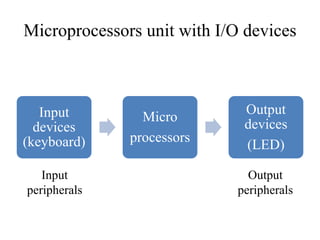
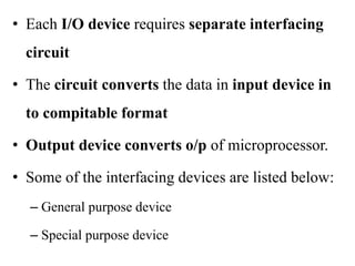
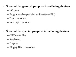
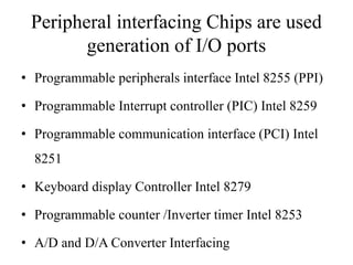
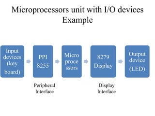
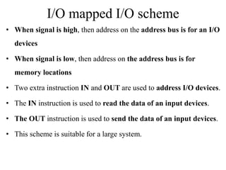
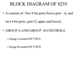
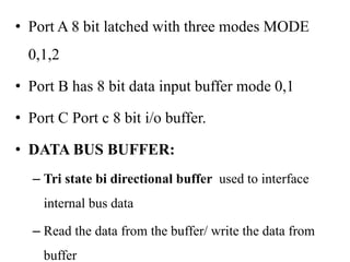
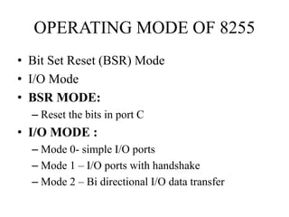
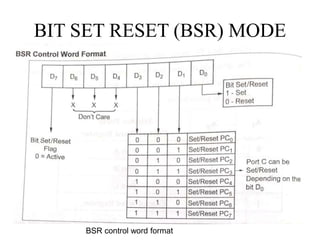
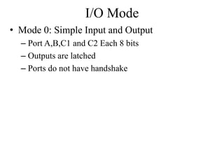
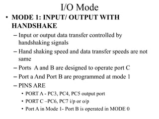
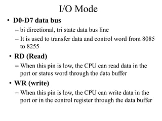
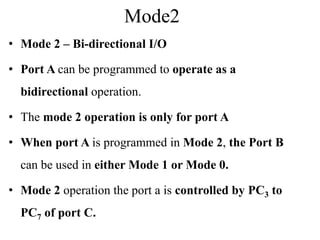
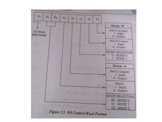
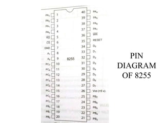
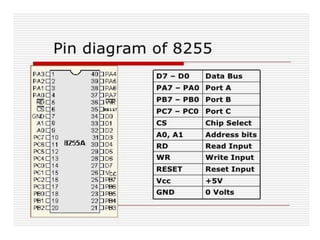
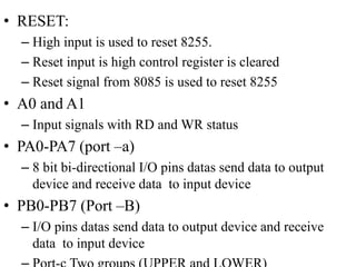
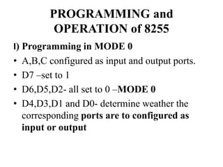
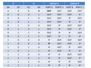
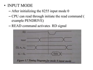
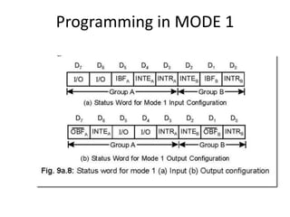
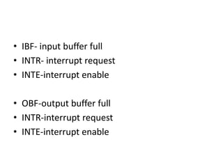
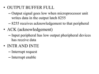
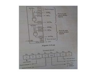
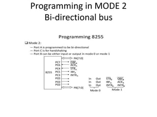
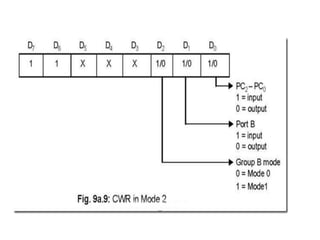
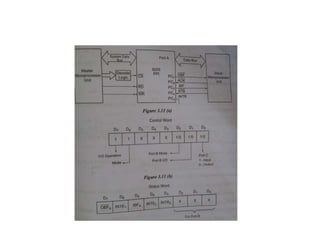
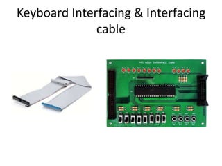
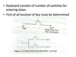
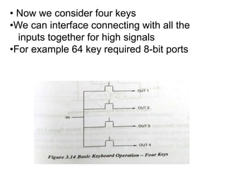
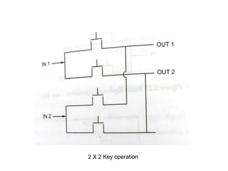
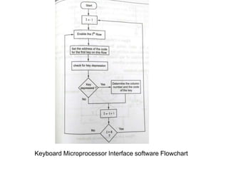
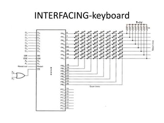
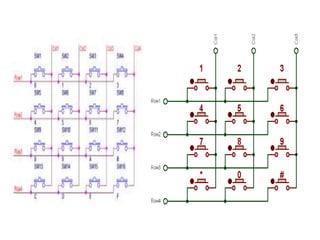
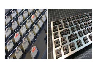
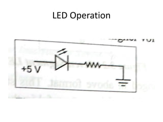
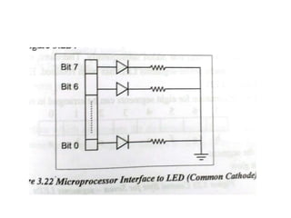
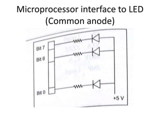
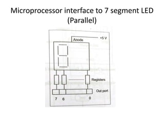
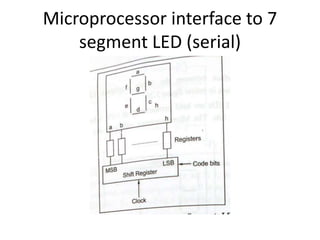
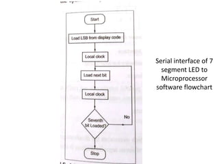
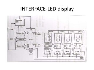
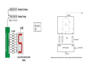
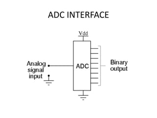
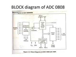
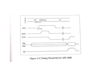
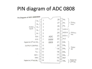
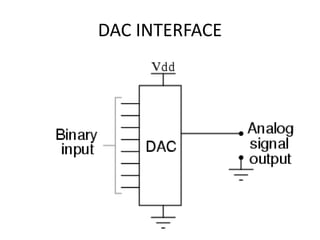
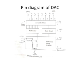
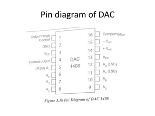
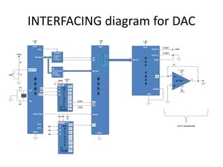
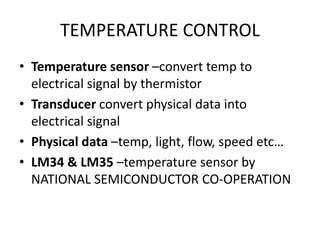
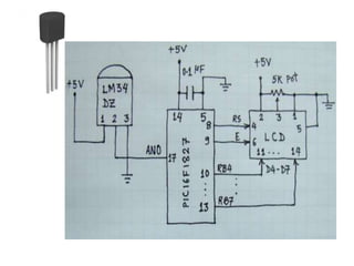
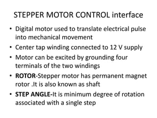
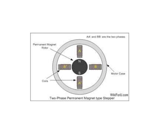
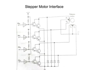
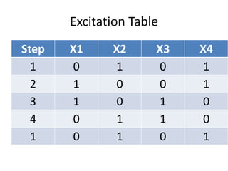
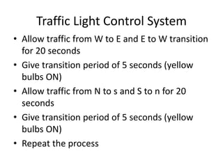
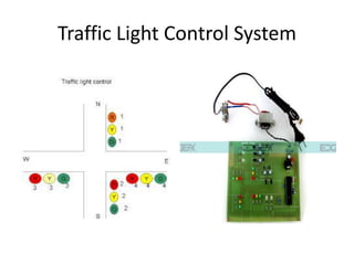
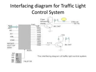
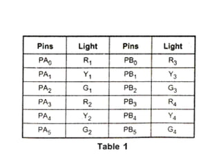
UNIT 3
PROGRAMMABLE PERIPERAL
INTERFACE
Content
• Introduction
• Architecture of 8255
• Keyboard interfacing
• LED display –interfacing
• ADC and DAC interface
• Temperature Control
• Stepper Motor Control
• Traffic Control interface
Introduction
• To communicate with the outside world,
microprocessor use peripherals (I/O devices)
• Input devices – Keyboards, A/D converters
etc.,
• Output devices – CRT, Printers, LEDs etc.,
• Peripherals are connected to the
microprocessors through electronic circuit
known as interfacing circuits.
Microprocessors unit with I/O devices
Input
devices
(keyboard)
Micro
processors
Output
devices
(LED)
Input
peripherals
Output
peripherals
• Each I/O device requires separate interfacing
circuit
• The circuit converts the data in input device in
to compitable format
• Output device converts o/p of microprocessor.
• Some of the interfacing devices are listed below:
– General purpose device
– Special purpose device
• Some of the general purpose interfacing devices
– I/O ports
– Programmable peripherals interface (PPI)
– D/A controllers
– Interrupt controller
• Some of the special purpose interfacing devices
– CRT controller
– Keyboard
– Display
– Floppy Disc controllers
Peripheral interfacing Chips are used
generation of I/O ports
• Programmable peripherals interface Intel 8255 (PPI)
• Programmable Interrupt controller (PIC) Intel 8259
• Programmable communication interface (PCI) Intel
8251
• Keyboard display Controller Intel 8279
• Programmable counter /Inverter timer Intel 8253
• A/D and D/A Converter Interfacing
Microprocessors unit with I/O devices
Example
Input
devices
(key
board)
PPI
8255
Micro
proce
ssors
8279
Display
Output
device
(LED)
Peripheral
Interface
Display
Interface
Address Space Partitioning
• The Microprocessors uses 16 bit wide address
bus for addressing memories and I/O devices.
• Using 16 bit wide address bus, it can access 216
= 64k bytes of memory and I/O devices
• Two schemes for the allocation of addresses to
memories and I/O devices
– Memory mapped I/O
– I/O mapped I/O
Memory mapped I/O
• It has only one address space
• Address space is defined as the set of all possible
addresses that a microprocessor can generate
• Some addresses assigned to memories and Some
addresses to I/O devices.
• Memory locations are assigned with addresses from
8000 to 80FF
• I/O devices are assigned with addresses from 8500
to 85FF
I/O mapped I/O scheme
• In this scheme, addresses assigned to
memories locations can also be assigned to
I/O devices
• Since the same address may be assigned to
memories locations or an I/O devices
• The microprocessor has a signal to distinguish
whether the address on the address bus is for
memories locations or an I/O devices
I/O mapped I/O scheme
• When signal is high, then address on the address bus is for an I/O
devices
• When signal is low, then address on the address bus is for
memory locations
• Two extra instruction IN and OUT are used to address I/O devices.
• The IN instruction is used to read the data of an input devices.
• The OUT instruction is used to send the data of an input devices.
• This scheme is suitable for a large system.
PROGRAMMABLE PERIPHERALS INTERFACE INTER 8255
(PPI) (16 mark)
• It is a multi port device.
• Ports can be programmed in variety ways
required by an operator.
• It is a general purpose programmable i/o devices
• It has 24 i/o pins 3*8 bit parallel ports.
• Port A, Port B, Port C,
• Port C can be groped in to two groups as 4 bits
FEATURES OF 8255
• 8255 is a widely used , programmable ,
parallel i/o devices
• It can easily transfer data under various
conditions
• Compatible with all micro processors
• Bit reset allows set reset of port C
• 8255 can operate 3 i/o modes
– Mode 0, Mode1 , mode 2
BLOCK DIAGRAM OF 8255
• It consists of Two 8 bit ports Port-a port – b, and
two 4 bit ports port C( upper and lower)
• GROUP-AAND GROUP –B CONTROLS:
– Group A control PC7-PC4
– Group B control PC3-PC0
• Port A 8 bit latched with three modes MODE
0,1,2
• Port B has 8 bit data input buffer mode 0,1
• Port C Port c 8 bit i/o buffer.
• DATA BUS BUFFER:
– Tri state bi directional buffer used to interface
internal bus data
– Read the data from the buffer/ write the data from
buffer
OPERATING MODE OF 8255
• Bit Set Reset (BSR) Mode
• I/O Mode
• BSR MODE:
– Reset the bits in port C
• I/O MODE :
– Mode 0- simple I/O ports
– Mode 1 – I/O ports with handshake
– Mode 2 – Bi directional I/O data transfer
BIT SET RESET (BSR) MODE
BSR control word format
I/O Mode
• Mode 0: Simple Input and Output
– Port A,B,C1 and C2 Each 8 bits
– Outputs are latched
– Ports do not have handshake
I/O Mode
• MODE 1: INPUT/ OUTPUT WITH
HANDSHAKE
– Input or output data transfer controlled by
handshaking signals
– Hand shaking speed and data transfer speeds are not
same
– Ports A and B are designed to operate port C
– Port a And Port B are programmed at mode 1
– PINS ARE
• PORT A - PC3, PC4, PC5 output port
• PORT C –PC6, PC7 i/p or o/p
• Port A in Mode 1- Port B is operated in MODE 0
I/O Mode
• D0-D7 data bus
– bi directional, tri state data bus line
– It is used to transfer data and control word from 8085
to 8255
• RD (Read)
– When this pin is low, the CPU can read data in the
port or status word through the data buffer
• WR (write)
– When this pin is low, the CPU can write data in the
port or in the control register through the data buffer
Mode2
• Mode 2 – Bi-directional I/O
• Port A can be programmed to operate as a
bidirectional operation.
• The mode 2 operation is only for port A
• When port A is programmed in Mode 2, the Port B
can be used in either Mode 1 or Mode 0.
• Mode 2 operation the port a is controlled by PC3 to
PC7 of port C.
PIN
DIAGRAM
OF 8255
• RESET:
– High input is used to reset 8255.
– Reset input is high control register is cleared
– Reset signal from 8085 is used to reset 8255
• A0 and A1
– Input signals with RD and WR status
• PA0-PA7 (port –a)
– 8 bit bi-directional I/O pins datas send data to output
device and receive data to input device
• PB0-PB7 (Port –B)
– I/O pins datas send data to output device and receive
data to input device
PROGRAMMING and
OPERATION of 8255
I) Programming in MODE 0
• A,B,C configured as input and output ports.
• D7 –set to 1
• D6,D5,D2- all set to 0 –MODE 0
• D4,D3,D1 and D0- determine weather the
corresponding ports are to configured as
input or output
A B GROUP A GROUP B
D4 D3 D1 D0 PORT A PORTC U PORT B PORT C L
0 0 0 0 OUT OUT OUT OUT
0 0 0 1 OUT OUT OUT IP
0 0 1 0 OUT OUT IP OUT
0 0 1 1 OUT OUT IP IP
0 1 0 0 OUT IP OUT OUT
0 1 0 1 OUT IP OUT IP
0 1 1 0 OUT IP IP OUT
0 1 1 1 OUT IP IP IP
1 0 0 0 IP OUT OUT OUT
1 0 0 1 IP OUT OUT IP
1 0 1 0 IP OUT IP OUT
1 0 1 1 IP OUT IP IP
1 1 0 0 IP IP OUT OUT
1 1 0 1 IP IP OUT IP
1 1 1 0 IP IP IP OUT
1 1 1 1 IP IP IP IP
• INPUT MODE
– After initializing the 8255 input mode 0
– CPU can read through initiate the read command (
example PENDRIVE)
– READ command activates RD signal
• OUTPUT MODE:
– After initializing the output mode 0
– CPU can write data in initiating command with
proper port address.
Programming in MODE 1
• IBF- input buffer full
• INTR- interrupt request
• INTE-interrupt enable
• OBF-output buffer full
• INTR-interrupt request
• INTE-interrupt enable
• OUTPUT BUFFER FULL
– Output signal goes low when microprocessor unit
writes data in the output latch 8255
– 8255 receives acknowledgement to that peripheral
• ACK (acknowledgement)
– Input peripheral has low output pheripheral devices
has receive data
• INTR AND INTE
– Interrupt request
– Interrupt enable
Programming in MODE 2
Bi-directional bus
• INPUT CONTROL SIGNAL:
– STB
• Low input signal enables PORT A
– IBF
• High input devices indicates loaded loaded on port a
– INTE2
• Interrupt enable with input buffer full.
• OUTPUT CONTROL SIGNAL:
– OBF
• Low output indicates cpu written data in port a
– ACK
• Low input signal enables output buffer of port A
Keyboard Interfacing & Interfacing
cable
• Keyboard consists of number of switches for
entering datas
• First of all location of key must be determined
• Now we consider four keys
•We can interface connecting with all the
inputs together for high signals
•For example 64 key required 8-bit ports
2 X 2 Key operation
Keyboard Microprocessor Interface software Flowchart
INTERFACING-keyboard
LED Operation
Microprocessor interface to LED
(Common anode)
Microprocessor interface to 7 segment LED
(Parallel)
Microprocessor interface to 7
segment LED (serial)
Serial interface of 7
segment LED to
Microprocessor
software flowchart
INTERFACE-LED display
ADC INTERFACE
BLOCK diagram of ADC 0808
PIN diagram of ADC 0808
DAC INTERFACE
Pin diagram of DAC
Pin diagram of DAC
INTERFACING diagram for DAC
TEMPERATURE CONTROL
• Temperature sensor –convert temp to
electrical signal by thermistor
• Transducer convert physical data into
electrical signal
• Physical data –temp, light, flow, speed etc…
• LM34 & LM35 –temperature sensor by
NATIONAL SEMICONDUCTOR CO-OPERATION
• LM34
• Output voltage is
linearly proportional to
Fahrenheit temp
• No external calibration
• 10mV for each degree
of Fahrenheit temp
• LM35
• Output voltage is
linearly proportional to
Celsius temp
• No external calibration
• 10mV for each degree
of Centigrate temp
STEPPER MOTOR CONTROL interface
• Digital motor used to translate electrical pulse
into mechanical movement
• Center tap winding connected to 12 V supply
• Motor can be excited by grounding four
terminals of the two windings
• ROTOR-Stepper motor has permanent magnet
rotor .It is also known as shaft
• STEP ANGLE-It is minimum degree of rotation
associated with a single step
Stepper Motor Interface
Excitation Table
Step X1 X2 X3 X4
1 0 1 0 1
2 1 0 0 1
3 1 0 1 0
4 0 1 1 0
1 0 1 0 1
Traffic Light Control System
• Allow traffic from W to E and E to W transition
for 20 seconds
• Give transition period of 5 seconds (yellow
bulbs ON)
• Allow traffic from N to s and S to n for 20
seconds
• Give transition period of 5 seconds (yellow
bulbs ON)
• Repeat the process
Traffic Light Control System
Interfacing diagram for Traffic Light
Control System
PPI-MECHATRONICS

PPI-MECHATRONICS

  • 1.
  • 2.
    Content • Introduction • Architectureof 8255 • Keyboard interfacing • LED display –interfacing • ADC and DAC interface • Temperature Control • Stepper Motor Control • Traffic Control interface
  • 3.
    Introduction • To communicatewith the outside world, microprocessor use peripherals (I/O devices) • Input devices – Keyboards, A/D converters etc., • Output devices – CRT, Printers, LEDs etc., • Peripherals are connected to the microprocessors through electronic circuit known as interfacing circuits.
  • 4.
    Microprocessors unit withI/O devices Input devices (keyboard) Micro processors Output devices (LED) Input peripherals Output peripherals
  • 5.
    • Each I/Odevice requires separate interfacing circuit • The circuit converts the data in input device in to compitable format • Output device converts o/p of microprocessor. • Some of the interfacing devices are listed below: – General purpose device – Special purpose device
  • 6.
    • Some ofthe general purpose interfacing devices – I/O ports – Programmable peripherals interface (PPI) – D/A controllers – Interrupt controller • Some of the special purpose interfacing devices – CRT controller – Keyboard – Display – Floppy Disc controllers
  • 7.
    Peripheral interfacing Chipsare used generation of I/O ports • Programmable peripherals interface Intel 8255 (PPI) • Programmable Interrupt controller (PIC) Intel 8259 • Programmable communication interface (PCI) Intel 8251 • Keyboard display Controller Intel 8279 • Programmable counter /Inverter timer Intel 8253 • A/D and D/A Converter Interfacing
  • 8.
    Microprocessors unit withI/O devices Example Input devices (key board) PPI 8255 Micro proce ssors 8279 Display Output device (LED) Peripheral Interface Display Interface
  • 9.
    Address Space Partitioning •The Microprocessors uses 16 bit wide address bus for addressing memories and I/O devices. • Using 16 bit wide address bus, it can access 216 = 64k bytes of memory and I/O devices • Two schemes for the allocation of addresses to memories and I/O devices – Memory mapped I/O – I/O mapped I/O
  • 10.
    Memory mapped I/O •It has only one address space • Address space is defined as the set of all possible addresses that a microprocessor can generate • Some addresses assigned to memories and Some addresses to I/O devices. • Memory locations are assigned with addresses from 8000 to 80FF • I/O devices are assigned with addresses from 8500 to 85FF
  • 11.
    I/O mapped I/Oscheme • In this scheme, addresses assigned to memories locations can also be assigned to I/O devices • Since the same address may be assigned to memories locations or an I/O devices • The microprocessor has a signal to distinguish whether the address on the address bus is for memories locations or an I/O devices
  • 12.
    I/O mapped I/Oscheme • When signal is high, then address on the address bus is for an I/O devices • When signal is low, then address on the address bus is for memory locations • Two extra instruction IN and OUT are used to address I/O devices. • The IN instruction is used to read the data of an input devices. • The OUT instruction is used to send the data of an input devices. • This scheme is suitable for a large system.
  • 13.
    PROGRAMMABLE PERIPHERALS INTERFACEINTER 8255 (PPI) (16 mark)
  • 14.
    • It isa multi port device. • Ports can be programmed in variety ways required by an operator. • It is a general purpose programmable i/o devices • It has 24 i/o pins 3*8 bit parallel ports. • Port A, Port B, Port C, • Port C can be groped in to two groups as 4 bits
  • 15.
    FEATURES OF 8255 •8255 is a widely used , programmable , parallel i/o devices • It can easily transfer data under various conditions • Compatible with all micro processors • Bit reset allows set reset of port C • 8255 can operate 3 i/o modes – Mode 0, Mode1 , mode 2
  • 16.
    BLOCK DIAGRAM OF8255 • It consists of Two 8 bit ports Port-a port – b, and two 4 bit ports port C( upper and lower) • GROUP-AAND GROUP –B CONTROLS: – Group A control PC7-PC4 – Group B control PC3-PC0
  • 17.
    • Port A8 bit latched with three modes MODE 0,1,2 • Port B has 8 bit data input buffer mode 0,1 • Port C Port c 8 bit i/o buffer. • DATA BUS BUFFER: – Tri state bi directional buffer used to interface internal bus data – Read the data from the buffer/ write the data from buffer
  • 18.
    OPERATING MODE OF8255 • Bit Set Reset (BSR) Mode • I/O Mode • BSR MODE: – Reset the bits in port C • I/O MODE : – Mode 0- simple I/O ports – Mode 1 – I/O ports with handshake – Mode 2 – Bi directional I/O data transfer
  • 19.
    BIT SET RESET(BSR) MODE BSR control word format
  • 20.
    I/O Mode • Mode0: Simple Input and Output – Port A,B,C1 and C2 Each 8 bits – Outputs are latched – Ports do not have handshake
  • 21.
    I/O Mode • MODE1: INPUT/ OUTPUT WITH HANDSHAKE – Input or output data transfer controlled by handshaking signals – Hand shaking speed and data transfer speeds are not same – Ports A and B are designed to operate port C – Port a And Port B are programmed at mode 1 – PINS ARE • PORT A - PC3, PC4, PC5 output port • PORT C –PC6, PC7 i/p or o/p • Port A in Mode 1- Port B is operated in MODE 0
  • 22.
    I/O Mode • D0-D7data bus – bi directional, tri state data bus line – It is used to transfer data and control word from 8085 to 8255 • RD (Read) – When this pin is low, the CPU can read data in the port or status word through the data buffer • WR (write) – When this pin is low, the CPU can write data in the port or in the control register through the data buffer
  • 23.
    Mode2 • Mode 2– Bi-directional I/O • Port A can be programmed to operate as a bidirectional operation. • The mode 2 operation is only for port A • When port A is programmed in Mode 2, the Port B can be used in either Mode 1 or Mode 0. • Mode 2 operation the port a is controlled by PC3 to PC7 of port C.
  • 25.
  • 27.
    • RESET: – Highinput is used to reset 8255. – Reset input is high control register is cleared – Reset signal from 8085 is used to reset 8255 • A0 and A1 – Input signals with RD and WR status • PA0-PA7 (port –a) – 8 bit bi-directional I/O pins datas send data to output device and receive data to input device • PB0-PB7 (Port –B) – I/O pins datas send data to output device and receive data to input device
  • 28.
    PROGRAMMING and OPERATION of8255 I) Programming in MODE 0 • A,B,C configured as input and output ports. • D7 –set to 1 • D6,D5,D2- all set to 0 –MODE 0 • D4,D3,D1 and D0- determine weather the corresponding ports are to configured as input or output
  • 29.
    A B GROUPA GROUP B D4 D3 D1 D0 PORT A PORTC U PORT B PORT C L 0 0 0 0 OUT OUT OUT OUT 0 0 0 1 OUT OUT OUT IP 0 0 1 0 OUT OUT IP OUT 0 0 1 1 OUT OUT IP IP 0 1 0 0 OUT IP OUT OUT 0 1 0 1 OUT IP OUT IP 0 1 1 0 OUT IP IP OUT 0 1 1 1 OUT IP IP IP 1 0 0 0 IP OUT OUT OUT 1 0 0 1 IP OUT OUT IP 1 0 1 0 IP OUT IP OUT 1 0 1 1 IP OUT IP IP 1 1 0 0 IP IP OUT OUT 1 1 0 1 IP IP OUT IP 1 1 1 0 IP IP IP OUT 1 1 1 1 IP IP IP IP
  • 30.
    • INPUT MODE –After initializing the 8255 input mode 0 – CPU can read through initiate the read command ( example PENDRIVE) – READ command activates RD signal
  • 31.
    • OUTPUT MODE: –After initializing the output mode 0 – CPU can write data in initiating command with proper port address.
  • 32.
  • 33.
    • IBF- inputbuffer full • INTR- interrupt request • INTE-interrupt enable • OBF-output buffer full • INTR-interrupt request • INTE-interrupt enable
  • 34.
    • OUTPUT BUFFERFULL – Output signal goes low when microprocessor unit writes data in the output latch 8255 – 8255 receives acknowledgement to that peripheral • ACK (acknowledgement) – Input peripheral has low output pheripheral devices has receive data • INTR AND INTE – Interrupt request – Interrupt enable
  • 36.
    Programming in MODE2 Bi-directional bus
  • 39.
    • INPUT CONTROLSIGNAL: – STB • Low input signal enables PORT A – IBF • High input devices indicates loaded loaded on port a – INTE2 • Interrupt enable with input buffer full. • OUTPUT CONTROL SIGNAL: – OBF • Low output indicates cpu written data in port a – ACK • Low input signal enables output buffer of port A
  • 40.
    Keyboard Interfacing &Interfacing cable
  • 41.
    • Keyboard consistsof number of switches for entering datas • First of all location of key must be determined
  • 42.
    • Now weconsider four keys •We can interface connecting with all the inputs together for high signals •For example 64 key required 8-bit ports
  • 43.
    2 X 2Key operation
  • 44.
  • 45.
  • 48.
  • 50.
    Microprocessor interface toLED (Common anode)
  • 52.
    Microprocessor interface to7 segment LED (Parallel)
  • 53.
    Microprocessor interface to7 segment LED (serial)
  • 54.
    Serial interface of7 segment LED to Microprocessor software flowchart
  • 55.
  • 57.
  • 58.
  • 60.
  • 62.
  • 63.
  • 64.
  • 65.
  • 66.
    TEMPERATURE CONTROL • Temperaturesensor –convert temp to electrical signal by thermistor • Transducer convert physical data into electrical signal • Physical data –temp, light, flow, speed etc… • LM34 & LM35 –temperature sensor by NATIONAL SEMICONDUCTOR CO-OPERATION
  • 67.
    • LM34 • Outputvoltage is linearly proportional to Fahrenheit temp • No external calibration • 10mV for each degree of Fahrenheit temp • LM35 • Output voltage is linearly proportional to Celsius temp • No external calibration • 10mV for each degree of Centigrate temp
  • 69.
    STEPPER MOTOR CONTROLinterface • Digital motor used to translate electrical pulse into mechanical movement • Center tap winding connected to 12 V supply • Motor can be excited by grounding four terminals of the two windings • ROTOR-Stepper motor has permanent magnet rotor .It is also known as shaft • STEP ANGLE-It is minimum degree of rotation associated with a single step
  • 71.
  • 72.
    Excitation Table Step X1X2 X3 X4 1 0 1 0 1 2 1 0 0 1 3 1 0 1 0 4 0 1 1 0 1 0 1 0 1
  • 73.
    Traffic Light ControlSystem • Allow traffic from W to E and E to W transition for 20 seconds • Give transition period of 5 seconds (yellow bulbs ON) • Allow traffic from N to s and S to n for 20 seconds • Give transition period of 5 seconds (yellow bulbs ON) • Repeat the process
  • 74.
  • 75.
    Interfacing diagram forTraffic Light Control System