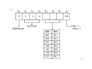
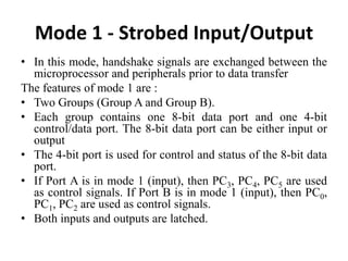
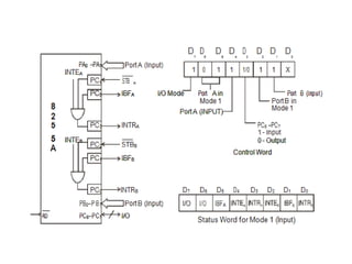
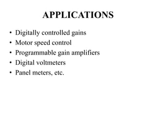
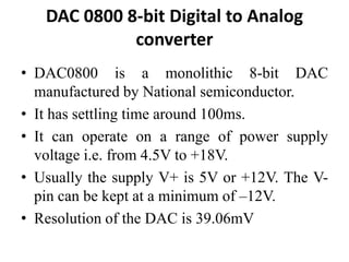
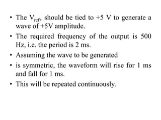
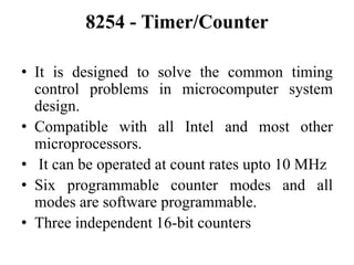
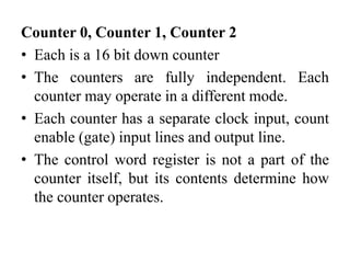
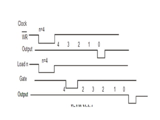
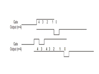
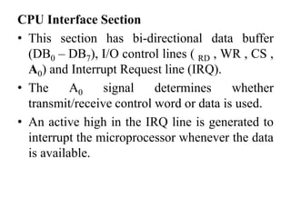
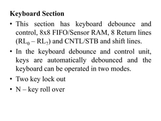
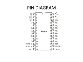
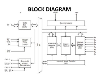
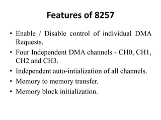
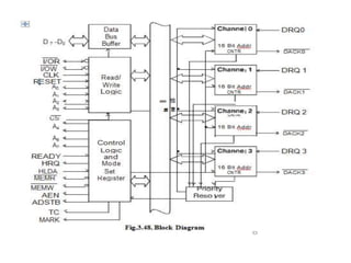
UNIT- 3
PERIPHERAL INTERFACING
Memory Interfacing
• While executing a program, the microprocessor
needs to access memory frequently to read
instruction code and data stored in memory; the
interfacing circuit enables that access.
• Memory has some signal requirements to write
into and read from its registers.
• Similary, the microprocessor initiates a set of
signals when it wants to read from and write into
memory.
I/O INTERFACING
• The Input/Output devices such as keyboards and
displays are the communication channels to the
outside world.
• Latches and buffers are used for I/O interfacing.
They once hardwired, perform only one function
(either as input device if it is buffer and as output
device if it is a latch). Thus limiting their
capabilities.
• To improve the overall system performance the
Intel has designed various programmable I/O
devices.
• Some of the peripheral devices developed by
Intel for 8085/8086/8088 based system are:
• 8255 - Parallel Communication Interface
• 8251 - Serial Communication Interface
• 8254 - Programmable Timer
• 8279 - Keyboard / Display Controller
• 8257 - DMA Controller
• 8259 - Programmable Interrupt Controller
• The microprocessor can communicate with
external world or other systems using two
types of communication interfaces. They are:
• Serial Communication Interface
• Parallel Communication Interface.
Serial Communication Interface
• The serial communication interface gets a byte
of data from the microprocessor and sends it
bit by bit to the other system serially or it
receives data bit by bit serially from the
external system.
• Then it converts the data into bytes and sends
to the microprocessor.
Parallel Communication Interface
• A parallel communication interface gets a byte
from the microprocessor and sends all the bits
in that byte simultaneously (parallel) to the
external system and vice-versa.
SERIAL COMMUNICATION INTERFACE
• The primary difference between parallel I/O and
serial I/O is the number of lines used for data
transfer; the parallel I/O uses the entire data bus
and serial I/O uses one data line.
• In serial I/O transmission the microprocessor
selects the peripheral through chip select ( CS )
and uses the control signals read to receive data
and write to transmit data.
• The address decoding can be either I/O-mapped
I/O or memory-mapped I/O.
• Serial data transmission is classified as
• Simplex
• Half duplex
• Full duplex
Simplex
• The data are transmitted in only one direction.
There is no possibility of data transfer in the
other direction.
• Example : Transmission from a computer to
the printer.
Half duplex
• The data are transmitted in both directions, but
not simultaneously.
• Example : Walky - Talky
Full duplex
• The data are transmitted in both directions
simultaneously.
• Example : Telephone
The data in the serial communication may be
sent in two formats:
• Asynchronous
• Synchronous
Synchronous Transmission
• In synchronous transmission, a receiver and
transmitter work in same speed and could be
synchronized.
• Both will use a common clock and start at the
same time
Asynchronous transmission
• The asynchronous transmission is character-
oriented. Each character carries the information of
the Start and Stop bits
• When no data are being transmitted, a receiver
stays high at logic 1, called Mark and logic 0 is
called Space.
• Transmission begins with one start bit (Low),
followed by 7 or 8 bits to represent a character
and 1 or 2 Stop bits (high).
• A start bit, character and stop bits are called as
Frame.
PARALLEL COMMUNICATION INTERFACE OR
(8255 A - Programmable Peripheral
Interface)
• It has a 3-state bi-directional 8-bit buffer which
interfaces the 8255A to the sys-tem data bus.
• It has 24 programmable I/O Pins.
• It reduces the external logic normally needed
to interface peripheral devices.
• It has two 8 bit ports: Port A, Port B, and two 4
bit ports: CUPPER and CLOWER.
• Available in 40-Pin DIP and 44-Pin PLCC.
OPERATING MODES
• It can be operated in two basic modes:
– Bit Set/Reset Mode
– I/O Mode
• I/O mode is further divided into 3 modes:
– Simple I/O mode (Mode 0)
– Strobed I/O mode (Mode 1)
– Bidirectional Data Transfer mode (Mode 2)
Pin diagram of 8255A
• The 8255 consists of Four sections namely
• Data Bus Buffer
• Read/Write Control Logic
• Group A Control
• Group B Control
DATA BUS BUFFER
• Used to interface the internal data bus of
8255A to the system data bus of 8085.
• Using IN or OUT instructions, CPU can read
or write the data from/to the data bus buffer.
• It can also be used to transfer control words
and status information between CPU and
8255A.
Read/Write Control Logic
• This block controls the Chip Selection ( CS ),
Read ( RD ) and Write ( WR ) operations.
• It consists of A0 and A1 signals which are
generally connected to the CPU address lines
A0 and A1 respectively.
• When CS (Chip Select) signal goes LOW,
different values of A0 and A1 select one of the
I/O ports or control register
• Group A : Port A and Most Significant Bits
(MSB) of Port C (PC4 – PC7)
• Group B : Port B and Least Significant Bits
(LSB) of Port C (PC0 – PC3)
• Port A: One 8-bit data output latch/buffer and
one 8-bit input latch buffer.
• Port B: One 8-bit data input/output latch/buffer.
• Port C: One 8-bit data output latch/buffer and
one 8-bit data input buffer. This port can be
divided into two 4-bit ports and it can be used for
the control signal outputs and status signal inputs
in conjunction with ports A and B.
BSR (Bit Set/Reset) Mode
• This mode is applicable only for Port C.
• A control word with bit D7 = 0 is recognized
as BSR control word.
• This control word can set or reset a single bit
in the Port C.
The I/O mode is divided into three modes
Mode 0, Mode 1 and Mode 2 as given below.
• Mode 0 – Basic I/O Mode
• Mode 1 – Strobed I/O Mode
• Mode 2 – Bi-directional data transfer mode
Mode 0 – Basic I/O mode
• The features of Mode 0 are :
• Two 8-bit ports (Port A, Port B) and two 4-bit
ports (Port CU, Port CL). Any port can be input
or output.
• Outputs are latched.
• Inputs are not latched.
Mode 1 - Strobed Input/Output
• In this mode, handshake signals are exchanged between the
microprocessor and peripherals prior to data transfer
The features of mode 1 are :
• Two Groups (Group A and Group B).
• Each group contains one 8-bit data port and one 4-bit
control/data port. The 8-bit data port can be either input or
output
• The 4-bit port is used for control and status of the 8-bit data
port.
• If Port A is in mode 1 (input), then PC3, PC4, PC5 are used
as control signals. If Port B is in mode 1 (input), then PC0,
PC1, PC2 are used as control signals.
• Both inputs and outputs are latched.
• STB (Strobe Input) – A “low” signal on this
pin indicates that the peripheral device has
transmitted a byte of data.
• The 8255A in response to STB , generates IBF
and INTR.
• IBF (Input Buffer Full) – A “high” signal
issued by 8255A is an acknowledge to indicate
that the input latch has received the data byte.
This is reset when the CPU reads the data.
• INTR (Interrupt Request) – This is an output
signal, used to interrupt the CPU. This will be
in active state when STB , IBF and INTE
(internal Flip-Flop) are all at logic 1. This will
be reset by the falling edge of RD signal.
• INTE (Interrupt Enable) – This is an Internal
Flip-Flop used to enable or disable the
generation of INTR signal. There are two Flip-
Flops INTEA and INTEB are set/reset using the
BSR mode.
Mode 2 – Bi-directional Data
Transfer Mode
• This mode provides a means for communicating
with a peripheral device or structure on a single 8-
bit bus for both transmitting and receiving data
(bidirectional bus I/O).
• The features of Mode 2 are :
• Used in Group A only.
• Port A only acts as bi-directional bus port
• Port C (PC3-PC7) is used for handshaking
purpose.
INTR (Interrupt Request):
• A high on this output can be used to interrupt
the CPU for input or output operations.
OBF(Output Buffer Full):
This signal will go LOW to indicate that the
CPU has written data out to Port A.
ACK(Acknowledge):
A LOW on this input enables the tri-state
output buffer of Port A to send out the data.
• Otherwise, the output buffer will be in the high
impedance state.
DIGITAL TO ANALOG
CONVERTERS (DAC)
• The digital to analog converters (DAC)
convert binary numbers into their analog
equivalent voltages or currents. Several
techniques are employed for digital to analog
conversion.
• Weighted resistor network
• R-2R ladder network
• Current output D/A converter
APPLICATIONS
• Digitally controlled gains
• Motor speed control
• Programmable gain amplifiers
• Digital voltmeters
• Panel meters, etc.
• Resolution: It is a change in analog output for
one LSB change in digital input.
(1/2n )*Vref
• 1/256*5 V=39.06 mV (since n=8 for 8-bit
DAC)
• Settling time: It is the time required for the
DAC to settle for a full scale code change.
DAC 0800 8-bit Digital to Analog
converter
• DAC0800 is a monolithic 8-bit DAC
manufactured by National semiconductor.
• It has settling time around 100ms.
• It can operate on a range of power supply
voltage i.e. from 4.5V to +18V.
• Usually the supply V+ is 5V or +12V. The V-
pin can be kept at a minimum of –12V.
• Resolution of the DAC is 39.06mV
• The Vref+ should be tied to +5 V to generate a
wave of +5V amplitude.
• The required frequency of the output is 500
Hz, i.e. the period is 2 ms.
• Assuming the wave to be generated
• is symmetric, the waveform will rise for 1 ms
and fall for 1 ms.
• This will be repeated continuously.
ANALOG TO DIGITAL INTERFACE
• ADC 0808/0809
8254 - Timer/Counter
• It is designed to solve the common timing
control problems in microcomputer system
design.
• Compatible with all Intel and most other
microprocessors.
• It can be operated at count rates upto 10 MHz
• Six programmable counter modes and all
modes are software programmable.
• Three independent 16-bit counters
Applications of 8254
• Real time clock
• Event-counter
• Digital one-shot
• Programmable rate generator
• Square wave generator
PIN DIAGRAM
BLOCK DIAGRAM
Data Bus Buffer
• This 3-state, bi-directional, 8-bit buffer is used
to interface the 8254 to the system bus.
Read/Write Logic
• The Read/Write logic accepts inputs from the
system bus and generates control signals for
the other functional blocks of the 8254.
• A1 and A0 select one of the three counters or
the control word register to be read
from/written into.
Control Word Register
• The control word register is selected by the
Read/Write logic when A1, A0=11.
• If the CPU then does a write operation to the
8254, the data is stored in the control word
register and is interpreted as a control word
used to define the operation of the counters.
• The control word register can only be written
to; status information is available with the
Read-Back command.
Counter 0, Counter 1, Counter 2
• Each is a 16 bit down counter
• The counters are fully independent. Each
counter may operate in a different mode.
• Each counter has a separate clock input, count
enable (gate) input lines and output line.
• The control word register is not a part of the
counter itself, but its contents determine how
the counter operates.
OPERATING MODES
• Mode 0: Interrupt On Terminal Count
• Mode 1: Hardware Retriggerable One-Shot
• Mode 2: Rate Generator
• Mode 3: Square Wave Mode
• Mode 4: Software Triggered Strobe
• Mode 5: Hardware Triggered Strobe
Mode 0: Interrupt On Terminal Count
• Mode 0 is typically used for event counting.
• After the control word is written, OUT is
initially low, and will remain low until the
counter reaches zero. OUT then goes high and
remains high until a new count or a new Mode
0 control word is written into the counter.
• GATE = 1 enables counting;
• GATE = 0 disables counting. GATE has no
effect on OUT
Mode 1: Hardware Re-triggerable
One-Shot
• OUT will be initially high. OUT will go low on the CLK pulse
following a trigger to begin the one-shot pulse, and will remain low
until the counter reaches zero.
• OUT will then go high and remain high until the CLK pulse after the
next trigger. Thus generating a one-shot pulse.
• After writing the control word and initial count, the counter is
armed.
• A trigger results in loading the counter and setting OUT low on the
next CLK pulse, thus starting the one-shot pulse. An initial count of
N will result in a one-shot pulse ‘N’ CLK cycles in duration.
Mode 2: Rate Generator
• This mode functions like a divide-by-N counter.
• It is typically used to generate a real time clock
interrupt.
• OUT will initially be high. When the initial count
has decremented to 1, OUT goes low for one CLK
pulse. OUT then goes high again, the counter
reloads the initial count and the process is
repeated.
• Mode 2 is periodic; the same sequence is repeated
indefinitely.
• For an initial count of N, the sequence repeats
every N CLK cycles.
Mode 3: Square Wave Mode
• Mode 3 is typically used for baud rate
generation.
• Mode 3 is similar to Mode 2 except for the
duty cycle of OUT. OUT will initially be high.
When half the initial count has expired, OUT
goes low for the remainder of the count.
• Mode 3 is periodic; the sequence above is
repeated indefinitely. An initial count of N
results in a square wave with a period of N
CLK cycles.
METHODS TO IMPLEMENT
MODE 3
Even counts:
• OUT is initially high. The initial count is loaded
on one CLK pulse and then is decremented by
two on succeeding CLK pulses. When the count
expires OUT changes value and the counter is
reloaded with the initial count. The above process
is repeated indefinitely.
Odd counts:
• For odd counts, OUT will be high for (N +1)/2
counts and low for (N - 1)/2 counts.
Mode 4: Software Triggered Strobe
• The output goes high on setting the mode.
After terminal count, the output goes low for
one clock period and then goes high again.
• In this mode the OUT is initially high; it goes
low for one clock period at the end of the
count. The count must be reloaded for
subsequent outputs.
Mode 5: Hardware Triggered Strobe
• This mode is similar to mode 4, but a trigger at
the gate initiates the counting.
• This mode is similar to mode 4, except that it
is triggered by the rising pulse at the gate.
• Initially the OUT is high and when the gate
pulse is triggered from low to high, the count
begins, at the end of the count, the OUT goes
low for one clock period.
Programming the 8254
Write Operations
• For each counter, the control word must be
written before the initial count is written.
• The initial count must follow the count format
specified in the control word (least significant
byte only, most significant byte only, or least
significant byte and then most significant
byte).
Read Operations
• It is often desirable to read the value of a
counter without disturbing the count in
progress. This is easily done in the 8254.
• There are three possible methods for reading
the counters:
• Simple read operation,
• Counter latch command, and
• Read-Back command.
CONTROL WORD FORMAT OF
8254
KEYBOARD/DISPLAY CONTROLLER
• Intel 8279 is an LSI device.
• It simultaneously drives the display of a system
and interfaces a keyboard with the
microprocessor.
• The keyboard display interface scans the
keyboard to identify if any key has been pressed
and sends the code of the pressed key to the
microprocessor.
• It also transmits the data received from
microprocessor to the display device.
Features of 8279
• 8279 has 3 input modes for keyboard interface
– Scanned keyboard mode
– Scanned sensor matrix mode
– Strobed input mode
• 8279 has 2 output modes for display interface
– Left entry
– Right entry
• It has two key depression modes
– 2 key lockout mode
– N key rollover mode
PIN DIAGRAM
Data Bus (D7 – D0) :
• All data and commands between the
microprocessor and 8279 are transmitted on these
lines.
RD (Read) :
Microprocessor reads the data/status from 8279.
WR (Write) :
Microprocessor writes the data to 8279.
A0 :
• A HIGH signal on this line indicates that the word
is a command or status. A LOW signal indicates
the data.
RESET :
• High signal in this pin resets the 8279. After
being reset, the 8279 is placed in the following
modes
• 16 x 8-bit character display –left entry
• Two key lock out
CS (Chip Select) :
A LOW signal on this input pin enables the
communication between 8279 and the
microprocessor.
IRQ (Interrupt Request) :
• The interrupt line goes low with each
FIFO/sensor RAM reads and returns high if
there is still information in the RAM.
SL0 – SL3 :
• Scan lines which are used to scan the key
switch or sensor matrix and the display digits.
• These lines can be either encoded (1 of 16) or
decoded (1 of 4).
RL0 – RL7 :
• Input return lines which are connected to the
scan lines through the keys or sensor switches.
• They have active internal pull-ups to keep
them high until a switch closure pull one low.
These also serve as an 8-bit input in the
strobed input mode.
SHIFT :
• It has an active internal pullup to keep it high
until a switch closure pulls it low.
CNTL/STB :
• For keyboard mode, this line is used as a control
input and stored like status on a key closure.
• The line is also the strobed line to enter the data
in to the FIFO in the strobed input mode.
OUT A0 – OUT A3, OUT B0 – OUT B3 :
• These two ports are the outputs for the 16´4
display refresh registers. These two ports may
also be considered as one 8-bit port.
• The two 4-bit ports may be blanked
independently.
BD :
This output is used to blank the display during
digit switching or by a display blanking
command.
Block Diagram of 8279
• The 8279 has the following four sections.
• CPU Interface Section
• Keyboard Section
• Scan Section
• Display Section
CPU Interface Section
• This section has bi-directional data buffer
(DB0 – DB7), I/O control lines ( RD , WR , CS ,
A0) and Interrupt Request line (IRQ).
• The A0 signal determines whether
transmit/receive control word or data is used.
• An active high in the IRQ line is generated to
interrupt the microprocessor whenever the data
is available.
Keyboard Section
• This section has keyboard debounce and
control, 8x8 FIFO/Sensor RAM, 8 Return lines
(RL0 – RL7) and CNTL/STB and shift lines.
• In the keyboard debounce and control unit,
keys are automatically debounced and the
keyboard can be operated in two modes.
• Two key lock out
• N – key roll over
• In the two key lock out mode, if two keys are
pressed simultaneously, the first key only
recognized.
• In the N-key roll over mode, it stores the codes of
simultaneous keys pressed in the internal buffer, it
can also be setup so that no key is recognized
until only one key remains pressed.
• The 8´8 FIFO/Sensor RAM consists of 8 registers
that are used to store eight keyboard entries.
• The return lines (RL0 – RL7) are connected to
eight columns of keyboard.
• The status of shift and CNTL/STB lines are stored
along with the key closure.
Scan Section
• This section has scan counter and four scan
lines (SL0–SL3).
• These lines are decoded by 4 to16 decoder to
generate 16 scan lines.
• Generally SL0 – SL3 are connected with the
rows of a matrix keyboard.
Display Section
• This section has two groups of output lines A0
– A3 and B0–B3.
• These lines are used to send data to display
drivers.
• BD line is used blank the display.
• It also has 16 x 8 display RAM.
Programming the 8279
INTERRUPT CONTROLLER
• The 8259A programmable interrupt controller
extends the hardware interrupt facility provided in
a microprocessor.
• It manages up to 8 vectored priority interrupts for
a processor.
• It has built-in features for expandability to other
8259A’s (up to 64 vectored priority interrupts).
• It is programmed by the system’s software as an
I/O peripheral.
Features of 8259 A
• It can manage 8 priority interrupts.
• By cascading 8259s it is possible to get 64
priority interrupts.
• It can be programmed to accept either the level
triggered or the edge triggered interrupt
request.
• Reading of interrupt request register (IRR) and
in-service register (ISR) through data bus.
VARIOUS MODES OF OPERATION
• Fully nested mode
• Special fully nested mode.
• Special mask mode
• Buffered mode
• Poll command mode
• Cascade mode with master or slave selection
• Automatic end-of-interrupt mode
PIN DIAGRAM
BLOCK DIAGRAM
Interrupt Request Register (IRR)
• The interrupts at the IR input lines are handled
by two registers in cascade, the Interrupt
Request Register (IRR) and the In-Service
Register (ISR).
• The IRR is used to store all the interrupt levels
which are requesting service.
In-Service Register (ISR)
• The ISR is used to store all the interrupt levels
which are being serviced.
Priority Resolver
• This logic block determines the priorities of
the bits set in the IRR. The highest priority is
selected and strobed into the corresponding bit
of the ISR during INTA pulse.
Interrupt Mask Register (IMR)
• The IMR stores the bits which mask the
interrupt lines to be masked. The IMR operates
on the IRR. Masking of a higher priority input
will not affect the interrupt request lines of
lower quality.
Data Bus Buffer
• This 3-state, bidirectional 8-bit buffer is used
to interface the 8259A to the system data bus.
Control words and status information are
transferred through the Data Bus Buffer.
Read/Write Control Logic
• The function of this block is to accept output
commands from the Microprocessor.
• It contains the Initialization Command Word
(ICW) registers and Operation Command
Word (OCW) registers which store the various
control formats for device operation.
• This function block also allows the status of
the 8259A to be transferred onto the data bus.
Cascade Buffer/Comparator
• This block is used to expand the number of
interrupt levels by cascading two or more 8259s.
• This function block stores and compares the IDs
of all 8259A’s used in the system.
• The associated three I/O pins (CAS0-2) are
outputs when the 8259A is used as a master and
are inputs when the 8259A is used as a slave.
• As a master, the 8259A sends the ID of the
interrupting slave device onto the CAS0±2 lines.
Control Logic
• This block has two pins INT and INTA.
INT (Interrupt)
• This output goes directly to the CPU interrupt
input. The voltage level on this line is designed to
be fully compatible with the 8080A, 8085A and
8086 input levels.
INTA (Interrupt Acknowledge)
• INTA pulses will cause the 8259A to release
vectoring information onto the data bus.
• The format of this data depends on the system
mode of the 8259A
PRIORITY MODES
• Fully Nested Mode
• This mode is entered after initialization unless
another mode is programmed.
• The interrupt requests are ordered in priority
from 0 through 7 (0 highest).
• When an interrupt is acknowledged the highest
priority request is determined and its vector
placed on the bus.
• Automatic End of Interrupt (AEOI) Mode
• If AEOI = 1 in ICW4, then the 8259A will operate in
AEOI mode continuously until reprogrammed by
ICW4.
• In this mode the 8259A will automatically perform a
non-specific EOI operation at the trailing edge of the
last interrupt acknowledge pulse.
• Automatic Rotation (Equal Priority Devices)
• In some applications there are a number of interrupting
devices of equal priority.
• In this mode a device after being serviced, receives the
lowest priority. So a device requesting an interrupt will
have to wait.
• In the worst case until each of 7 other devices are
serviced at most once.
• Specific Rotation (Specific Priority)
• The programmer can change priorities by
programming the bottom priority and thus fixing
all other priorities; i.e., if IR4 is programmed as
the lowest priority device, then IR5 will have the
highest one.
• Special Mask Mode
• In the special mask mode, when a mask bit is set
in OCW1, it inhibits further interrupts at that level
and enables interrupts from all other levels (lower
as well as higher) that are not masked.
• Thus, any interrupts may be selectively enabled
by loading the mask register.
• Poll Command
• In poll mode the INT output functions as it
normally does.
• The microprocessor should ignore this output.
• This can be accomplished either by not
connecting the INT output or by masking
interrupts within the microprocessor, thereby
disabling its interrupt input.
• Service to devices is achieved by software
using a poll command.
• Special Fully Nest Mode
• This mode will be used in the case of a big
system where cascading is used, and the
priority has to be conserved within each slave.
• In this case the fully nested mode will be
programmed to the master.
• Buffered Mode
• When the 8259A is used in a large system
where bus driving buffers are required on the
data bus and the cascading mode is used, there
exists the problem of enabling buffers.
• This modification forces the use of software
programming to determine whether the 8259A
is a master or a slave.
INITIALIZATION COMMAND WORD
ICW 1
• A write command issued to the 8259 with A0=0
and D4=1 is interpreted as ICW 1, which starts the
initialization sequence. It specifies,
• Single or Multiple 8259s in the system.
• 4 or 8 bit, interval between the interrupt vector
Locations.
• The address bits A7–A5 of the CALL instruction.
• Edge triggered or Level triggered interrupts.
• ICW 4 is needed or not.
ICW 2
• ICW 2 is issued following, ICW 1 with A0 = 1
• ICW 2 specified the high-order byte of the
CALL instruction.
• Since A0 input of 8259 is connected to address
line A1, ICW1 should be addressed to ‘C0’ H
& ICW 2 should be addressed to ‘C2’ H
• ICW 3 :
• ICW 3 is required if there is more than one
8259 in the system and if they are cascaded.
• An ICW 3 operation loads a slave register in
the 8259.
• The format of the byte to be loaded as an ICW
3 for a MASTER 8259 or a SLAVE
• ICW 4 :
• It is loaded only if the D0 bit of ICW 1 is set.
• It specifies,
• Whether to use special fully nested mode or non
special fully nested mode.
• Whether to use buffered mode or non buffered
mode.
• Whether to use Automatic EOI or Normal EOI.
• CPU used – 8085 or 8086 / 8088
OCW
• After intialization, the 8259 is ready to process IRs.
• However during operation, it might be necessary to
change the mode of processing the interrupt OCWs
which are used for this purpose.
• They may be loaded anytime after the initialization of
8259 to operate in various interrupt modes.
These modes are
• Fully nested mode
• Rotating Binary mode
• Special Mask mode
• Polled mode
OCW1
• Issued with A0=1, used to mask the interrupts.
To enable all the IR lines, the command word
is 00 H.
OCW 2:
• A write command with A0 = 1 and D4D3=00 is
interpreted as OCW2.
• R–Rotate
• SL–Select Level
• EOI - End of Interrupt
• The R, SL, EOI bits control the Rotate and
End of Interrupt Modes and combinations of
the two.
OCW 3 :
• OCW 3 is used to read the status of the
registers and to set or reset the Special Mask
and Polled Modes.
8257-PROGRAMMABLE DMA
CONTROLLER
• The ability of an I/O sub system is to transfer
data to and from a memory subsystem, which
is used for high speed data transfer.
• Ex : Data transfer between a floppy disk and
memory.
DMA Controller :
• It is a device that can control data transfer
between an I/O subsystem and a memory
subsystem without the help of CPU.
DMA Operation sequence
• Once interface is ready to receive data, DMA request is
made.
• Bus request is made by the DMA.
• Bus grant is returned by the processor.
• DMA places address on the address bus.
• DMA request is acknowledged.
• Memory places data on the data bus.
• Interface latches data.
• Bus request is dropped and control is returned to the
processor
• Bus grant is dropped by the processor.
Features of 8257
• Enable / Disable control of individual DMA
Requests.
• Four Independent DMA channels - CH0, CH1,
CH2 and CH3.
• Independent auto-intialization of all channels.
• Memory to memory transfer.
• Memory block initialization.
Data Bus Buffer :
• It is a tri-state, bidirectional, 8 bit buffer which
interfaces the 8257 to the system data bus.
• In the slave mode, it is used to transfer data
between microprocessor and internal registers
of 8257.
• In master mode, it is used to send higher byte
address (A8–A15) on the data bus.
Read/Write Logic :
• During DMA cycles (ie, Master mode) the
Read/Write logic generates the I/O read and
memory write (DMA write cycle) or I/O Write
and Memory read (DMA read cycle) signals
which control the data transfer between
peripheral and memory device.
DMA Channels
• The 8257 provides four identical channels
labelled CH0, CH1, CH2 and CH3. Each channel
has two-16 bit registers
• DMA address register
• Terminal Count register
DMA address Register:
• It specifies the address of the first memory
location to be accessed. It is necessary to load
valid memory address in the DMA address
register before channel is enabled.
Terminal Count Register :
• The value loaded into the low order 14 bits (C13–
C0) of TCR specifies the number of DMA cycles
minus one (N–1) before TC output is activated.
TERMINAL COUNT REGISTER
Control Logic :
• It controls the sequence of operations during
all DMA cycles (DMA read, DMA write,
DMA verify) by generating the appropriate
control signals and the 16-bit address that
specifies the memory location to be accessed.
• It consists of mode set register and status
register.
Mode Set Register
• LSB 4 bits are the enable 4 DMA channels
• MSB 4 bits are the enable Autoload, TC Stop,
Extended Write, Rotating Priority Modes.
• It is normally programmed by the CPU after
initializing the DMA address registers and
terminal count registers.
• It is cleared by RESET input, this disabling all
options, inhibiting all channels, and preventing
bus conflicts on power-up.
STATUS BIT REGISTER
• It indicates which channels have reached a
terminal count condition and includes the update
flag.
• The TC status bit = 1, terminal count has been
reached for that channel.
• TC bit remains set until the status register is read
or the 8257 is reset.
• Update flag = 1, 8257 is executing update cycle.
• In update cycle 8257 load parameters in channel 3
to channel 2.
Priority Resolver :
• It resolves the peripherals request. It can be
programmed to work in two modes, either in
fixed mode or rotating priority mode.

UNIT- 3.pptx

  • 1.
  • 2.
    Memory Interfacing • Whileexecuting a program, the microprocessor needs to access memory frequently to read instruction code and data stored in memory; the interfacing circuit enables that access. • Memory has some signal requirements to write into and read from its registers. • Similary, the microprocessor initiates a set of signals when it wants to read from and write into memory.
  • 3.
    I/O INTERFACING • TheInput/Output devices such as keyboards and displays are the communication channels to the outside world. • Latches and buffers are used for I/O interfacing. They once hardwired, perform only one function (either as input device if it is buffer and as output device if it is a latch). Thus limiting their capabilities. • To improve the overall system performance the Intel has designed various programmable I/O devices.
  • 4.
    • Some ofthe peripheral devices developed by Intel for 8085/8086/8088 based system are: • 8255 - Parallel Communication Interface • 8251 - Serial Communication Interface • 8254 - Programmable Timer • 8279 - Keyboard / Display Controller • 8257 - DMA Controller • 8259 - Programmable Interrupt Controller
  • 5.
    • The microprocessorcan communicate with external world or other systems using two types of communication interfaces. They are: • Serial Communication Interface • Parallel Communication Interface.
  • 6.
    Serial Communication Interface •The serial communication interface gets a byte of data from the microprocessor and sends it bit by bit to the other system serially or it receives data bit by bit serially from the external system. • Then it converts the data into bytes and sends to the microprocessor.
  • 7.
    Parallel Communication Interface •A parallel communication interface gets a byte from the microprocessor and sends all the bits in that byte simultaneously (parallel) to the external system and vice-versa.
  • 8.
    SERIAL COMMUNICATION INTERFACE •The primary difference between parallel I/O and serial I/O is the number of lines used for data transfer; the parallel I/O uses the entire data bus and serial I/O uses one data line. • In serial I/O transmission the microprocessor selects the peripheral through chip select ( CS ) and uses the control signals read to receive data and write to transmit data. • The address decoding can be either I/O-mapped I/O or memory-mapped I/O.
  • 9.
    • Serial datatransmission is classified as • Simplex • Half duplex • Full duplex
  • 10.
    Simplex • The dataare transmitted in only one direction. There is no possibility of data transfer in the other direction. • Example : Transmission from a computer to the printer. Half duplex • The data are transmitted in both directions, but not simultaneously. • Example : Walky - Talky
  • 11.
    Full duplex • Thedata are transmitted in both directions simultaneously. • Example : Telephone The data in the serial communication may be sent in two formats: • Asynchronous • Synchronous
  • 12.
    Synchronous Transmission • Insynchronous transmission, a receiver and transmitter work in same speed and could be synchronized. • Both will use a common clock and start at the same time
  • 14.
    Asynchronous transmission • Theasynchronous transmission is character- oriented. Each character carries the information of the Start and Stop bits • When no data are being transmitted, a receiver stays high at logic 1, called Mark and logic 0 is called Space. • Transmission begins with one start bit (Low), followed by 7 or 8 bits to represent a character and 1 or 2 Stop bits (high). • A start bit, character and stop bits are called as Frame.
  • 16.
    PARALLEL COMMUNICATION INTERFACEOR (8255 A - Programmable Peripheral Interface) • It has a 3-state bi-directional 8-bit buffer which interfaces the 8255A to the sys-tem data bus. • It has 24 programmable I/O Pins. • It reduces the external logic normally needed to interface peripheral devices. • It has two 8 bit ports: Port A, Port B, and two 4 bit ports: CUPPER and CLOWER. • Available in 40-Pin DIP and 44-Pin PLCC.
  • 17.
    OPERATING MODES • Itcan be operated in two basic modes: – Bit Set/Reset Mode – I/O Mode • I/O mode is further divided into 3 modes: – Simple I/O mode (Mode 0) – Strobed I/O mode (Mode 1) – Bidirectional Data Transfer mode (Mode 2)
  • 18.
  • 19.
    • The 8255consists of Four sections namely • Data Bus Buffer • Read/Write Control Logic • Group A Control • Group B Control
  • 21.
    DATA BUS BUFFER •Used to interface the internal data bus of 8255A to the system data bus of 8085. • Using IN or OUT instructions, CPU can read or write the data from/to the data bus buffer. • It can also be used to transfer control words and status information between CPU and 8255A.
  • 22.
    Read/Write Control Logic •This block controls the Chip Selection ( CS ), Read ( RD ) and Write ( WR ) operations. • It consists of A0 and A1 signals which are generally connected to the CPU address lines A0 and A1 respectively. • When CS (Chip Select) signal goes LOW, different values of A0 and A1 select one of the I/O ports or control register
  • 25.
    • Group A: Port A and Most Significant Bits (MSB) of Port C (PC4 – PC7) • Group B : Port B and Least Significant Bits (LSB) of Port C (PC0 – PC3) • Port A: One 8-bit data output latch/buffer and one 8-bit input latch buffer. • Port B: One 8-bit data input/output latch/buffer. • Port C: One 8-bit data output latch/buffer and one 8-bit data input buffer. This port can be divided into two 4-bit ports and it can be used for the control signal outputs and status signal inputs in conjunction with ports A and B.
  • 27.
    BSR (Bit Set/Reset)Mode • This mode is applicable only for Port C. • A control word with bit D7 = 0 is recognized as BSR control word. • This control word can set or reset a single bit in the Port C.
  • 29.
    The I/O modeis divided into three modes Mode 0, Mode 1 and Mode 2 as given below. • Mode 0 – Basic I/O Mode • Mode 1 – Strobed I/O Mode • Mode 2 – Bi-directional data transfer mode
  • 31.
    Mode 0 –Basic I/O mode • The features of Mode 0 are : • Two 8-bit ports (Port A, Port B) and two 4-bit ports (Port CU, Port CL). Any port can be input or output. • Outputs are latched. • Inputs are not latched.
  • 33.
    Mode 1 -Strobed Input/Output • In this mode, handshake signals are exchanged between the microprocessor and peripherals prior to data transfer The features of mode 1 are : • Two Groups (Group A and Group B). • Each group contains one 8-bit data port and one 4-bit control/data port. The 8-bit data port can be either input or output • The 4-bit port is used for control and status of the 8-bit data port. • If Port A is in mode 1 (input), then PC3, PC4, PC5 are used as control signals. If Port B is in mode 1 (input), then PC0, PC1, PC2 are used as control signals. • Both inputs and outputs are latched.
  • 35.
    • STB (StrobeInput) – A “low” signal on this pin indicates that the peripheral device has transmitted a byte of data. • The 8255A in response to STB , generates IBF and INTR. • IBF (Input Buffer Full) – A “high” signal issued by 8255A is an acknowledge to indicate that the input latch has received the data byte. This is reset when the CPU reads the data.
  • 36.
    • INTR (InterruptRequest) – This is an output signal, used to interrupt the CPU. This will be in active state when STB , IBF and INTE (internal Flip-Flop) are all at logic 1. This will be reset by the falling edge of RD signal. • INTE (Interrupt Enable) – This is an Internal Flip-Flop used to enable or disable the generation of INTR signal. There are two Flip- Flops INTEA and INTEB are set/reset using the BSR mode.
  • 37.
    Mode 2 –Bi-directional Data Transfer Mode • This mode provides a means for communicating with a peripheral device or structure on a single 8- bit bus for both transmitting and receiving data (bidirectional bus I/O). • The features of Mode 2 are : • Used in Group A only. • Port A only acts as bi-directional bus port • Port C (PC3-PC7) is used for handshaking purpose.
  • 39.
    INTR (Interrupt Request): •A high on this output can be used to interrupt the CPU for input or output operations. OBF(Output Buffer Full): This signal will go LOW to indicate that the CPU has written data out to Port A. ACK(Acknowledge): A LOW on this input enables the tri-state output buffer of Port A to send out the data. • Otherwise, the output buffer will be in the high impedance state.
  • 41.
    DIGITAL TO ANALOG CONVERTERS(DAC) • The digital to analog converters (DAC) convert binary numbers into their analog equivalent voltages or currents. Several techniques are employed for digital to analog conversion. • Weighted resistor network • R-2R ladder network • Current output D/A converter
  • 42.
    APPLICATIONS • Digitally controlledgains • Motor speed control • Programmable gain amplifiers • Digital voltmeters • Panel meters, etc.
  • 43.
    • Resolution: Itis a change in analog output for one LSB change in digital input. (1/2n )*Vref • 1/256*5 V=39.06 mV (since n=8 for 8-bit DAC) • Settling time: It is the time required for the DAC to settle for a full scale code change.
  • 44.
    DAC 0800 8-bitDigital to Analog converter • DAC0800 is a monolithic 8-bit DAC manufactured by National semiconductor. • It has settling time around 100ms. • It can operate on a range of power supply voltage i.e. from 4.5V to +18V. • Usually the supply V+ is 5V or +12V. The V- pin can be kept at a minimum of –12V. • Resolution of the DAC is 39.06mV
  • 47.
    • The Vref+should be tied to +5 V to generate a wave of +5V amplitude. • The required frequency of the output is 500 Hz, i.e. the period is 2 ms. • Assuming the wave to be generated • is symmetric, the waveform will rise for 1 ms and fall for 1 ms. • This will be repeated continuously.
  • 49.
    ANALOG TO DIGITALINTERFACE • ADC 0808/0809
  • 50.
    8254 - Timer/Counter •It is designed to solve the common timing control problems in microcomputer system design. • Compatible with all Intel and most other microprocessors. • It can be operated at count rates upto 10 MHz • Six programmable counter modes and all modes are software programmable. • Three independent 16-bit counters
  • 51.
    Applications of 8254 •Real time clock • Event-counter • Digital one-shot • Programmable rate generator • Square wave generator
  • 52.
  • 53.
  • 54.
    Data Bus Buffer •This 3-state, bi-directional, 8-bit buffer is used to interface the 8254 to the system bus. Read/Write Logic • The Read/Write logic accepts inputs from the system bus and generates control signals for the other functional blocks of the 8254. • A1 and A0 select one of the three counters or the control word register to be read from/written into.
  • 55.
    Control Word Register •The control word register is selected by the Read/Write logic when A1, A0=11. • If the CPU then does a write operation to the 8254, the data is stored in the control word register and is interpreted as a control word used to define the operation of the counters. • The control word register can only be written to; status information is available with the Read-Back command.
  • 56.
    Counter 0, Counter1, Counter 2 • Each is a 16 bit down counter • The counters are fully independent. Each counter may operate in a different mode. • Each counter has a separate clock input, count enable (gate) input lines and output line. • The control word register is not a part of the counter itself, but its contents determine how the counter operates.
  • 57.
    OPERATING MODES • Mode0: Interrupt On Terminal Count • Mode 1: Hardware Retriggerable One-Shot • Mode 2: Rate Generator • Mode 3: Square Wave Mode • Mode 4: Software Triggered Strobe • Mode 5: Hardware Triggered Strobe
  • 58.
    Mode 0: InterruptOn Terminal Count • Mode 0 is typically used for event counting. • After the control word is written, OUT is initially low, and will remain low until the counter reaches zero. OUT then goes high and remains high until a new count or a new Mode 0 control word is written into the counter. • GATE = 1 enables counting; • GATE = 0 disables counting. GATE has no effect on OUT
  • 60.
    Mode 1: HardwareRe-triggerable One-Shot • OUT will be initially high. OUT will go low on the CLK pulse following a trigger to begin the one-shot pulse, and will remain low until the counter reaches zero. • OUT will then go high and remain high until the CLK pulse after the next trigger. Thus generating a one-shot pulse. • After writing the control word and initial count, the counter is armed. • A trigger results in loading the counter and setting OUT low on the next CLK pulse, thus starting the one-shot pulse. An initial count of N will result in a one-shot pulse ‘N’ CLK cycles in duration.
  • 62.
    Mode 2: RateGenerator • This mode functions like a divide-by-N counter. • It is typically used to generate a real time clock interrupt. • OUT will initially be high. When the initial count has decremented to 1, OUT goes low for one CLK pulse. OUT then goes high again, the counter reloads the initial count and the process is repeated. • Mode 2 is periodic; the same sequence is repeated indefinitely. • For an initial count of N, the sequence repeats every N CLK cycles.
  • 64.
    Mode 3: SquareWave Mode • Mode 3 is typically used for baud rate generation. • Mode 3 is similar to Mode 2 except for the duty cycle of OUT. OUT will initially be high. When half the initial count has expired, OUT goes low for the remainder of the count. • Mode 3 is periodic; the sequence above is repeated indefinitely. An initial count of N results in a square wave with a period of N CLK cycles.
  • 65.
    METHODS TO IMPLEMENT MODE3 Even counts: • OUT is initially high. The initial count is loaded on one CLK pulse and then is decremented by two on succeeding CLK pulses. When the count expires OUT changes value and the counter is reloaded with the initial count. The above process is repeated indefinitely. Odd counts: • For odd counts, OUT will be high for (N +1)/2 counts and low for (N - 1)/2 counts.
  • 67.
    Mode 4: SoftwareTriggered Strobe • The output goes high on setting the mode. After terminal count, the output goes low for one clock period and then goes high again. • In this mode the OUT is initially high; it goes low for one clock period at the end of the count. The count must be reloaded for subsequent outputs.
  • 69.
    Mode 5: HardwareTriggered Strobe • This mode is similar to mode 4, but a trigger at the gate initiates the counting. • This mode is similar to mode 4, except that it is triggered by the rising pulse at the gate. • Initially the OUT is high and when the gate pulse is triggered from low to high, the count begins, at the end of the count, the OUT goes low for one clock period.
  • 71.
    Programming the 8254 WriteOperations • For each counter, the control word must be written before the initial count is written. • The initial count must follow the count format specified in the control word (least significant byte only, most significant byte only, or least significant byte and then most significant byte).
  • 72.
    Read Operations • Itis often desirable to read the value of a counter without disturbing the count in progress. This is easily done in the 8254. • There are three possible methods for reading the counters: • Simple read operation, • Counter latch command, and • Read-Back command.
  • 73.
  • 74.
    KEYBOARD/DISPLAY CONTROLLER • Intel8279 is an LSI device. • It simultaneously drives the display of a system and interfaces a keyboard with the microprocessor. • The keyboard display interface scans the keyboard to identify if any key has been pressed and sends the code of the pressed key to the microprocessor. • It also transmits the data received from microprocessor to the display device.
  • 75.
    Features of 8279 •8279 has 3 input modes for keyboard interface – Scanned keyboard mode – Scanned sensor matrix mode – Strobed input mode • 8279 has 2 output modes for display interface – Left entry – Right entry • It has two key depression modes – 2 key lockout mode – N key rollover mode
  • 76.
  • 77.
    Data Bus (D7– D0) : • All data and commands between the microprocessor and 8279 are transmitted on these lines. RD (Read) : Microprocessor reads the data/status from 8279. WR (Write) : Microprocessor writes the data to 8279. A0 : • A HIGH signal on this line indicates that the word is a command or status. A LOW signal indicates the data.
  • 78.
    RESET : • Highsignal in this pin resets the 8279. After being reset, the 8279 is placed in the following modes • 16 x 8-bit character display –left entry • Two key lock out CS (Chip Select) : A LOW signal on this input pin enables the communication between 8279 and the microprocessor.
  • 79.
    IRQ (Interrupt Request): • The interrupt line goes low with each FIFO/sensor RAM reads and returns high if there is still information in the RAM. SL0 – SL3 : • Scan lines which are used to scan the key switch or sensor matrix and the display digits. • These lines can be either encoded (1 of 16) or decoded (1 of 4).
  • 80.
    RL0 – RL7: • Input return lines which are connected to the scan lines through the keys or sensor switches. • They have active internal pull-ups to keep them high until a switch closure pull one low. These also serve as an 8-bit input in the strobed input mode. SHIFT : • It has an active internal pullup to keep it high until a switch closure pulls it low.
  • 81.
    CNTL/STB : • Forkeyboard mode, this line is used as a control input and stored like status on a key closure. • The line is also the strobed line to enter the data in to the FIFO in the strobed input mode. OUT A0 – OUT A3, OUT B0 – OUT B3 : • These two ports are the outputs for the 16´4 display refresh registers. These two ports may also be considered as one 8-bit port. • The two 4-bit ports may be blanked independently.
  • 82.
    BD : This outputis used to blank the display during digit switching or by a display blanking command. Block Diagram of 8279 • The 8279 has the following four sections. • CPU Interface Section • Keyboard Section • Scan Section • Display Section
  • 84.
    CPU Interface Section •This section has bi-directional data buffer (DB0 – DB7), I/O control lines ( RD , WR , CS , A0) and Interrupt Request line (IRQ). • The A0 signal determines whether transmit/receive control word or data is used. • An active high in the IRQ line is generated to interrupt the microprocessor whenever the data is available.
  • 86.
    Keyboard Section • Thissection has keyboard debounce and control, 8x8 FIFO/Sensor RAM, 8 Return lines (RL0 – RL7) and CNTL/STB and shift lines. • In the keyboard debounce and control unit, keys are automatically debounced and the keyboard can be operated in two modes. • Two key lock out • N – key roll over
  • 87.
    • In thetwo key lock out mode, if two keys are pressed simultaneously, the first key only recognized. • In the N-key roll over mode, it stores the codes of simultaneous keys pressed in the internal buffer, it can also be setup so that no key is recognized until only one key remains pressed. • The 8´8 FIFO/Sensor RAM consists of 8 registers that are used to store eight keyboard entries. • The return lines (RL0 – RL7) are connected to eight columns of keyboard. • The status of shift and CNTL/STB lines are stored along with the key closure.
  • 88.
    Scan Section • Thissection has scan counter and four scan lines (SL0–SL3). • These lines are decoded by 4 to16 decoder to generate 16 scan lines. • Generally SL0 – SL3 are connected with the rows of a matrix keyboard.
  • 89.
    Display Section • Thissection has two groups of output lines A0 – A3 and B0–B3. • These lines are used to send data to display drivers. • BD line is used blank the display. • It also has 16 x 8 display RAM.
  • 90.
  • 98.
    INTERRUPT CONTROLLER • The8259A programmable interrupt controller extends the hardware interrupt facility provided in a microprocessor. • It manages up to 8 vectored priority interrupts for a processor. • It has built-in features for expandability to other 8259A’s (up to 64 vectored priority interrupts). • It is programmed by the system’s software as an I/O peripheral.
  • 99.
    Features of 8259A • It can manage 8 priority interrupts. • By cascading 8259s it is possible to get 64 priority interrupts. • It can be programmed to accept either the level triggered or the edge triggered interrupt request. • Reading of interrupt request register (IRR) and in-service register (ISR) through data bus.
  • 100.
    VARIOUS MODES OFOPERATION • Fully nested mode • Special fully nested mode. • Special mask mode • Buffered mode • Poll command mode • Cascade mode with master or slave selection • Automatic end-of-interrupt mode
  • 101.
  • 102.
  • 103.
    Interrupt Request Register(IRR) • The interrupts at the IR input lines are handled by two registers in cascade, the Interrupt Request Register (IRR) and the In-Service Register (ISR). • The IRR is used to store all the interrupt levels which are requesting service.
  • 104.
    In-Service Register (ISR) •The ISR is used to store all the interrupt levels which are being serviced. Priority Resolver • This logic block determines the priorities of the bits set in the IRR. The highest priority is selected and strobed into the corresponding bit of the ISR during INTA pulse.
  • 105.
    Interrupt Mask Register(IMR) • The IMR stores the bits which mask the interrupt lines to be masked. The IMR operates on the IRR. Masking of a higher priority input will not affect the interrupt request lines of lower quality. Data Bus Buffer • This 3-state, bidirectional 8-bit buffer is used to interface the 8259A to the system data bus. Control words and status information are transferred through the Data Bus Buffer.
  • 106.
    Read/Write Control Logic •The function of this block is to accept output commands from the Microprocessor. • It contains the Initialization Command Word (ICW) registers and Operation Command Word (OCW) registers which store the various control formats for device operation. • This function block also allows the status of the 8259A to be transferred onto the data bus.
  • 107.
    Cascade Buffer/Comparator • Thisblock is used to expand the number of interrupt levels by cascading two or more 8259s. • This function block stores and compares the IDs of all 8259A’s used in the system. • The associated three I/O pins (CAS0-2) are outputs when the 8259A is used as a master and are inputs when the 8259A is used as a slave. • As a master, the 8259A sends the ID of the interrupting slave device onto the CAS0±2 lines.
  • 108.
    Control Logic • Thisblock has two pins INT and INTA. INT (Interrupt) • This output goes directly to the CPU interrupt input. The voltage level on this line is designed to be fully compatible with the 8080A, 8085A and 8086 input levels. INTA (Interrupt Acknowledge) • INTA pulses will cause the 8259A to release vectoring information onto the data bus. • The format of this data depends on the system mode of the 8259A
  • 109.
    PRIORITY MODES • FullyNested Mode • This mode is entered after initialization unless another mode is programmed. • The interrupt requests are ordered in priority from 0 through 7 (0 highest). • When an interrupt is acknowledged the highest priority request is determined and its vector placed on the bus.
  • 110.
    • Automatic Endof Interrupt (AEOI) Mode • If AEOI = 1 in ICW4, then the 8259A will operate in AEOI mode continuously until reprogrammed by ICW4. • In this mode the 8259A will automatically perform a non-specific EOI operation at the trailing edge of the last interrupt acknowledge pulse. • Automatic Rotation (Equal Priority Devices) • In some applications there are a number of interrupting devices of equal priority. • In this mode a device after being serviced, receives the lowest priority. So a device requesting an interrupt will have to wait. • In the worst case until each of 7 other devices are serviced at most once.
  • 111.
    • Specific Rotation(Specific Priority) • The programmer can change priorities by programming the bottom priority and thus fixing all other priorities; i.e., if IR4 is programmed as the lowest priority device, then IR5 will have the highest one. • Special Mask Mode • In the special mask mode, when a mask bit is set in OCW1, it inhibits further interrupts at that level and enables interrupts from all other levels (lower as well as higher) that are not masked. • Thus, any interrupts may be selectively enabled by loading the mask register.
  • 112.
    • Poll Command •In poll mode the INT output functions as it normally does. • The microprocessor should ignore this output. • This can be accomplished either by not connecting the INT output or by masking interrupts within the microprocessor, thereby disabling its interrupt input. • Service to devices is achieved by software using a poll command.
  • 113.
    • Special FullyNest Mode • This mode will be used in the case of a big system where cascading is used, and the priority has to be conserved within each slave. • In this case the fully nested mode will be programmed to the master.
  • 114.
    • Buffered Mode •When the 8259A is used in a large system where bus driving buffers are required on the data bus and the cascading mode is used, there exists the problem of enabling buffers. • This modification forces the use of software programming to determine whether the 8259A is a master or a slave.
  • 115.
  • 116.
    ICW 1 • Awrite command issued to the 8259 with A0=0 and D4=1 is interpreted as ICW 1, which starts the initialization sequence. It specifies, • Single or Multiple 8259s in the system. • 4 or 8 bit, interval between the interrupt vector Locations. • The address bits A7–A5 of the CALL instruction. • Edge triggered or Level triggered interrupts. • ICW 4 is needed or not.
  • 118.
    ICW 2 • ICW2 is issued following, ICW 1 with A0 = 1 • ICW 2 specified the high-order byte of the CALL instruction. • Since A0 input of 8259 is connected to address line A1, ICW1 should be addressed to ‘C0’ H & ICW 2 should be addressed to ‘C2’ H
  • 120.
    • ICW 3: • ICW 3 is required if there is more than one 8259 in the system and if they are cascaded. • An ICW 3 operation loads a slave register in the 8259. • The format of the byte to be loaded as an ICW 3 for a MASTER 8259 or a SLAVE
  • 122.
    • ICW 4: • It is loaded only if the D0 bit of ICW 1 is set. • It specifies, • Whether to use special fully nested mode or non special fully nested mode. • Whether to use buffered mode or non buffered mode. • Whether to use Automatic EOI or Normal EOI. • CPU used – 8085 or 8086 / 8088
  • 124.
    OCW • After intialization,the 8259 is ready to process IRs. • However during operation, it might be necessary to change the mode of processing the interrupt OCWs which are used for this purpose. • They may be loaded anytime after the initialization of 8259 to operate in various interrupt modes. These modes are • Fully nested mode • Rotating Binary mode • Special Mask mode • Polled mode
  • 125.
    OCW1 • Issued withA0=1, used to mask the interrupts. To enable all the IR lines, the command word is 00 H.
  • 126.
    OCW 2: • Awrite command with A0 = 1 and D4D3=00 is interpreted as OCW2. • R–Rotate • SL–Select Level • EOI - End of Interrupt • The R, SL, EOI bits control the Rotate and End of Interrupt Modes and combinations of the two.
  • 128.
    OCW 3 : •OCW 3 is used to read the status of the registers and to set or reset the Special Mask and Polled Modes.
  • 129.
    8257-PROGRAMMABLE DMA CONTROLLER • Theability of an I/O sub system is to transfer data to and from a memory subsystem, which is used for high speed data transfer. • Ex : Data transfer between a floppy disk and memory. DMA Controller : • It is a device that can control data transfer between an I/O subsystem and a memory subsystem without the help of CPU.
  • 130.
    DMA Operation sequence •Once interface is ready to receive data, DMA request is made. • Bus request is made by the DMA. • Bus grant is returned by the processor. • DMA places address on the address bus. • DMA request is acknowledged. • Memory places data on the data bus. • Interface latches data. • Bus request is dropped and control is returned to the processor • Bus grant is dropped by the processor.
  • 131.
    Features of 8257 •Enable / Disable control of individual DMA Requests. • Four Independent DMA channels - CH0, CH1, CH2 and CH3. • Independent auto-intialization of all channels. • Memory to memory transfer. • Memory block initialization.
  • 134.
    Data Bus Buffer: • It is a tri-state, bidirectional, 8 bit buffer which interfaces the 8257 to the system data bus. • In the slave mode, it is used to transfer data between microprocessor and internal registers of 8257. • In master mode, it is used to send higher byte address (A8–A15) on the data bus.
  • 135.
    Read/Write Logic : •During DMA cycles (ie, Master mode) the Read/Write logic generates the I/O read and memory write (DMA write cycle) or I/O Write and Memory read (DMA read cycle) signals which control the data transfer between peripheral and memory device.
  • 136.
    DMA Channels • The8257 provides four identical channels labelled CH0, CH1, CH2 and CH3. Each channel has two-16 bit registers • DMA address register • Terminal Count register DMA address Register: • It specifies the address of the first memory location to be accessed. It is necessary to load valid memory address in the DMA address register before channel is enabled. Terminal Count Register : • The value loaded into the low order 14 bits (C13– C0) of TCR specifies the number of DMA cycles minus one (N–1) before TC output is activated.
  • 137.
  • 138.
    Control Logic : •It controls the sequence of operations during all DMA cycles (DMA read, DMA write, DMA verify) by generating the appropriate control signals and the 16-bit address that specifies the memory location to be accessed. • It consists of mode set register and status register.
  • 139.
    Mode Set Register •LSB 4 bits are the enable 4 DMA channels • MSB 4 bits are the enable Autoload, TC Stop, Extended Write, Rotating Priority Modes. • It is normally programmed by the CPU after initializing the DMA address registers and terminal count registers. • It is cleared by RESET input, this disabling all options, inhibiting all channels, and preventing bus conflicts on power-up.
  • 141.
    STATUS BIT REGISTER •It indicates which channels have reached a terminal count condition and includes the update flag. • The TC status bit = 1, terminal count has been reached for that channel. • TC bit remains set until the status register is read or the 8257 is reset. • Update flag = 1, 8257 is executing update cycle. • In update cycle 8257 load parameters in channel 3 to channel 2.
  • 143.
    Priority Resolver : •It resolves the peripherals request. It can be programmed to work in two modes, either in fixed mode or rotating priority mode.